Design
of
a three-dimensional gap-coupled
suspended substrate stripline bandpass filter
Y.-C. Chiang C.-K.C. Tzuang
s.
s uI n d e x i n g term: Filters andfiltering
Abstract: A three-dimensional gap-coupled sus- pended substrate stripline (SSS) bandpass filter, based on the modified configuration of the classic end-coupled filter, is presented. It consists of printed half-wavelength resonators placed on the same and/or the opposite sides of the suspended substrate. These resonators orient themselves in arbitrary directions. Such an arrangment makes the new filter highly flexible to interface with other microwave subcircuit modules. The filter is con- structed in a bent channelised housing that sup- presses any possibility of exciting higher-order modes, except the dominant quasi-TEM mode of propagation. Consequently, the channelised filter is free from any coupling between itself and other microwave circuit components within the system. Two look-up tables, derived from a variational three-dimensional quasi-TEM spectral-domain analysis of the discontinuity problems associated with the adjacent gap-coupled resonators, are incorporated into the computer-aided design of the new filter. The de-embedded discontinuity parameters are validated by comparing them with those obtained by experiment and full-wave approaches for the microstrip open-end and the SSS end-coupled problems, respectively. The measured results for the experimental 21-22 GHz bandpass filter agree very well with the theoretic predictions considering the conductor losses (5.57 x lo-’ dB/mm) of the SSS. It has less than 1.4 dB insertion loss and greater than 10dB return loss in the passband.
1 Introduction
The suspended substrate stripline (SSS) has been widely adopted in a variety of microwave and millimetre-wave filter designs [1-111. When compared with other planar or quasiplanar transmission lines, the SSS has the follow- ing merits: high unloaded Q, low-loss [l-61, insensitivity to temperature variation, as most of the electromagnetic energy of the SSS is essentially distributed in the air [l, 21, wider bandwidth [l-3, 5-8, 111, and broadband low-loss transition to a rectangular waveguide [7-101. Paper 8915H (ElZ), first received 4th December 1991 and in revised
form 22nd April 1992
The authors are with the Institute of Electrical Communication Engin- eering, Microelectronic and Information Science Research Centre, National Chiao Tung Universlty, 1 0 0 1 Ta Hsueh Road, Hsinchu, Taiwan, R.O.C.
376
Given a required impedance level, e.g. 50 R, the SSS is wider than most stripline-based planar or quasiplanar transmission lines integrated on the same printed-circuit substrate. This makes the SSS filters highly reproducible at low cost, using conventional photolithography tech- nologies.
Among various SSS filters reported [l-113, Rhodes and Dean developed a design approach incorporating the mixed lumped and distributed circuits [l-31. Using such an approach as a basis, they reported several broadband lowpass, highpass and bandpass filters operated at fre- quencies ranging from 0.5 to 40 GHz. By series or paral- lel connecting two or more lowpass and highpass filters, various broadband SSS filters, such as diplexers and multiplexers, were also reported.
The highpass filters designed by Rhodes and Dean 11-31 often mandate the use of strongly coupling ele- ments for certain broadband applications. Therefore the broadside-coupled SSSs are applied to meet such needs. As the filter performance is highly dependent on these broadside SSS coupling elements, the precise determ- ination of the dimensions of the coupling elements becomes one of the key issues for designing a high- performance broadband filter. Rhodes and Dean also employed the microwave circuit model proposed by Zysman and Johnson [12], who developed the equivalent circuit representation of the inhomogeneous parallel- coupled lines using quasi-TEM approximations, to analyse the symmetric broadside-coupled SSSs. The total fringing field effects of the sides and ends of the strips on the broadside-coupled SSSs, however, were approximated using the results obtained previously in Reference 3. By adopting the same technique, Mobbs and Rhodes [4] used the SSS broadside-coupled structures connecting with the high-impedance transmission lines to approx- imate the series LC circuit elements in a bandpass filter prototype. Based on such an approach, a 5 - 5 5 GHz bandpass filter, with more than 20 dB return loss and less
The authors would like to thank C.-D. Chen and J.-T. Kuo for their great help in providing the theoretic values of the complex propagation con- stant and the cut-off frequency of the first higher- order mode of the suspended substrate stripline. Thanks are also due to Steve Cheng for his assist- ance in obtaining the experimental results. This work was supported by the National Science Council, R.O.C., in part under Grant NSC81- 0404-E009-120 and in part under Contract CS80- 0210-D001-21.
than 1 dB insertion loss in the passband, was reported [4]. Losch and Malherbe extended the work of Zysman and Johnson by including the effect of the open-end fringing capacitances in the expressions of the effective dielectric constants for even the odd modes, respectively. Accordingly, they have designed and tested a 2-9 GHz psuedo-high-pass filter with a maximum 0.4 dB insertion loss [SI.
The circuit models developed by Zysman and Johnson were unsuitable for application in distributed filter syn- thesis [6]. To remedy the problem, Levy theorised a new equivalent circuit model of the inhomogeneous coupled line section, which consisted of a pair of series-connected unit elements in series with two open-circuited stubs and two uncoupled transmission lines. By using such an approach, a 6-18 GHz pseudo-high-pass filter with inser- tion loss less than 1 dB was demonstrated [6].
On the other hand, the concept of admittance inverters was applied to design the parallel-coupled and end- coupled SSS bandpass filters 17-11] with operating fre- quencies up to millimetre-wave (30-300 GHz). Rubin and Hislop used two step impedance resonators, replacing the first and last parallel-coupled resonators in a 28-37 GHz parallel-coupled bandpass filter, to achieve 28% frac- tional bandwidth [7]. Ton et al. further adopted the syn- thesis technique developed by Rhodes [ 131, and designed an 18-30 GHz parallel-coupled SSS filter with 50% frac- tional bandwidth, using high-resolution photolith- ography printed circuit board technology [SI. The end-coupled filters are rather lengthy in comparison with other types of printed circuit filter, but are suitable for higher microwave frequencies where large size is some- times advantageous. For instance, Nguyen and Chang reported the end-coupled SSS filter with passband at 32- 35 GHz [9], and Dougherty reported a three-resonator end-coupled SSS filter operated at 45 GHz [lo]. To avoid difficulty in increasing the bandwidth of the end- coupled filter, Tzuang er al. reported a broadside end- coupled SSS filter which easily achieved 30"h fractional bandwidth in K-band [l
11.
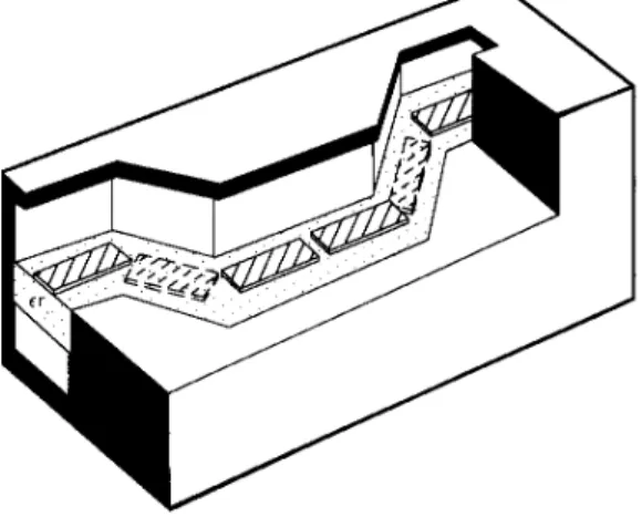
In contrast to the conventional colinear realisations of the end-coupled [9, lo] or broadside end-coupled [11] SSS filters, a new three-dimensional implementation of the gap-coupled SSS bandpass filter is shown in Fig. 1 .
The half-wavelength resonators of this filter are located on the same and/or the opposite sides of the suspended substrate and can orient themselves in any arbitrary direction. Because the coupling between the adjacent res- onators can be either end-coupled or broadside-coupled in arbitrary angles, the new filter configuration is named gap-coupled to reflect realistically its physical structure. The evolution from the conventional design to the new structure makes the filter much more complicated in shape, The new filter, however, has the following merits: It is highly flexible to interface itself with other micro- wave or millimetre-wave subcircuits in a communication system, because the resonators can change their orienta- tion. Secondly, the new filter configuration is channelised in a controlled way, i.e. all the cutoff frequencies of the higher-order modes are far beyond the desired upper stopband frequency. Thus, only the quasi-TEM mode and higher-order evanescent modes are allowed to exist in the channelised filter. These evanescent modes quickly attenuate nearby any discontinuities associated with the filter. Thus, no cross-coupling between the channelised filter and any other microwave components can exist in system integration. Furthermore, the well-developed filter synthesis technique assuming a TEM mode of propaga-
I E E P R O C E E D I N G S - H . Vol. 139, No. 4, A U G U S T 1992
tion can be applied here with confidence. This makes the filter characteristics highly predictable in both passband and stopband frequencies
Fig. 1 Three-dimensional implementation of the channelised gap- coupled suspended substrate stripline bandpassfilter
The SSS resonators with solid lines are on the tap surface of the suspended sub- strate. those with broken lines are on the bottom side of the substrate. The reson- ators can orient themselves in any arbitrary direction
The asymmetric gap-coupled discontinuities inherently present in the filter shown in Fig. 1, however, cannot possibly be determined by the above-mentioned equival- ent circuit approaches 11-61, Instead, a de-embedding procedure based on the three-dimensional quasi-TEM spectral-domain approach (SDA), which is the extended form of the two-dimensional SDA reported by Itoh [14],
is incorporated in our computer-aided design (CAD) program and will be described in Section 2. To ensure the accuracy of the de-embedded discontinuity parameters, a new set of two-dimensional basis functions to describe the charge distribution on the assumed infinitely thin metal strip is used.
The validity of the de-embedded discontinuity param- eters obtained by the three-dimensional quasi-TEM SDA is confirmed in Section 2.3 by comparing the theoretic results against the published data for the microstrip open-end and SSS end-coupled problems. This also demonstrates the fact that the static equivalent capa- citances of discontinuities in many planar waveguides supporting quasi-TEM modes will result in data having very good agreement with measurements as reported by Naghed and Wolff [lS].
Section 3 describes the filter design procedure as out- lined by Matthaei et al. [16] for a 21-22GHz three- resonator bandpass filter prototype, with its input and output ports located at the same reference plane. Such a filter has essentially zero compressed length. Section 4 confirms the accuracy of the design approach presented here by experimental evaluation of the prototype. The overall photolithography resolution tolerance for the fab- ricated filter is less than 0.02 mm. No tuning was neces- sary for the desired filter characteristics. The trial filter shows excellent agreement between the predicted filter performance and the measured data in both passband and stopband.
2 De-embedding of discontinuity parameters of gap-coupled resonators based on
three-dimensional quasi-TEM SDA
Fig. 2a shows the top view and the longitudinal-section view of a hypothetical three-resonator gap-coupled
371
bandpass filter. The side walls of the channelised housing are reshaped to be rectangular with dimension a x b. The lower and upper ground planes are kept the same. The three resonators are designated as R i , R i + and R i + , in
at reference planes 1 (2) and 1'(2), i.e. Bmi(BSi+J and B p d B p i + l ) , are critical to the first-time success of the filter design without any tuning. As the symmetry in the con- ventional colinear realisation of the end-coupled filter no
PEC' a . . .
-~
.
... .... ................. ... ... .... .... ................. .... .... . . . . i n a t o r ' R , ' , . , _ .,. ' , . ' . ' . ' . ' . . . . . . . . . . . .. .. .. .. . . . . . . . . . . . . . . . . . . . . . . ..
t . ' . ' . . . .. . .. .. . .. .. . .. .. .. .. . ..: . . . ' . . . ' . top view resonator R,+, resonator R,+2 b _ - - - e- _ _
I l - * - _ l .. .. .. .. .. .. .. . . . . . . . t . , ' . , ' . , ' . . . . . . . .. .. .. .. .. . . '.( .. . . . . . . . . .. ..t'
" resonat% R, E l hl longitudinal-section view 0 2 : i 2L-
e,+,+
k-- 9,+2-+ b Fig. 2The side walls of the channelised housing are reshaped to k rectangular. with dimension a x b The lower and upper ground planes are kept the same
r? Top view and longitudinal-section view of the hlter. resonators located at L = h , and L = h , + h, are shown by broken and solid lines, resPectiVelY b Equivalent il-circuit representation of R , , RE, I and R , , in a
Hypothetical three-resonator gap-coupled bandpass filter
Fig. 2a, respectively. Resonator R i , drawn in broken lines, is located at z = h i . Resonators R i + l and R i + , ,
drawn in solid lines, are located at z = h ,
+
h,. Let Piand P , + I be located at the central end points of the adjacent gap-coupled resonators, respectively. The rela- tive position between the adjacent gap-coupled reson- ators Ri and R i + l , for example, is described by the four gap discontinuity parameters t i , $ i , ui and v i . Parameter t , is the vertical distance between the adjacent resonators along the z direction, and only two values can be chosen, either ti = 0 or ti = h,. The former implies that the adjacent resonators are on the same side of the substrate, whereas the latter implies that they are on opposite sides.
$ i is the angle between the centrelines of the projection of
the resonator Ri and that of the resonator R i + l in the horizontal x-y plane. The value of uXoi) is determined by subtracting the x-component (y-component) value of the projected point P , from that of point P i + Therefore the values of ui and vi can be either positive or negative. The central point of the resonator R i + l projected in the x-y plane is denoted as (xi+
,,
y i +longer exists in Fig. 2a, an accurate and reliable method to de-embed the discontinuity parameters must be devel- oped,
Section 2.1 briefly describes how to obtain an accurate capacitance matrix by employing the three-dimensional quasi-TEM SDA. Followed by a conventional method for de-embedding the discontinuity parameters assuming quasi-TEM mode [ l l , 171, Section 2.2 explains how the susceptance parameters in the n-circuit of the gap- coupled discontinuities shown in Fig. 2 are obtained. The validity check of the de-embedding process described here is performed in Section 2.3. The results confirm the accuracy of our approach. Finally, Section 2.4 plots the discontinuity parameters necessary for carrying out the experimental filter design described in the following section.
2.1 Three-dimensional quasi- TEM spectral-domain
Under the quasi-TEM assumption, we only need to solve the laplace equation in an electrically shielded enclosure,
domain, we will work in the Fourier transform domain and introduce the two-dimensional Fourier transform of the potential function @ ( x , y , z )
q m , n, 2) = d x
1
dy% Y , 2)x sin [(mrr/a)x] sin [(nn/b)y]
m = l , 2 ,..., cc n = l , 2 ,..., cc ( 1 )
so that the partial differential equation (Laplace equation) becomes an ordinary differential equation through the previous transformation.
d Z
(mn/a)’ - (nn/b)’
1
6 ( m ,
n, z ) = 0where U and b are the dimensions of the housing bounded by perfectly conducting side walls, as shown in Fig. 2a. By imposing the boundary conditions at z = h , and z = h ,
+
h , in solving eqn. 2, one may obtain the following coupled algebraic equations:R N,
G l
l(m.n),E
?Am, n)+
Gl2(m, n )C
?Am, n )I = I , = R + l
= V(l)
+
iql) ( 3 4= V(2)
+
C(2) (3b)where
p j
is the unknown charge distribution on the jth resonator; R is the number of resonators located at z = hi; (N, - Rlis the number of resonators located at z = h ,+
h, and V ( 1 ) and i32) are the Fourier transform of the given potentials on the resonators and equal to zero outside the resonators at z = h, and z = h ,+
h,, respec- tively. Similarly, 6(l) and ii(2) are the Fourier transform of the potential distributions outside resonators and equal to zero on the resonators.C l , ,
e,,,
e,,
andG,,
are Green’s functions in the Fourier transform domain. To solve the unknown charge distributionF 3 ,
the Galerkin method is applied [14]. The unknown charge distribution on a resonator can be expressed as(4) 1 = 1
where
q
represents the number of basis functions used to expand the unknown charge distribution on the jth res- onatoj, a: is the unknown coefficient to be determined andt:
is the Fourier transform of an assumed space domain charge distribution t;(x, y), or the so-called basis functions. Substituting eqn. 4 into eqn. 3 and taking the inner prod_ucts of the resulting equations with weighting functionsti,
for k = 1, 2,...,
N , , and s = 1, 2, ...,G,
then one may obtain the following ?; x
7;
matrix equations for the unknown coefficient a:, j = I, 2, _ _ _ , N,, and t = 1 , 2, ...,
7;:
M - z N - J ~ R J l m = 1 n = 1 t:(m,n)[Gll(m,n)Z j = l r = l C a : c { m , n ) I E E PROCEEDINGS-H, Vol. 139, N o . 4, A U G U S T 1992 where =fr46
[ d x l d y t ; ( x , y)V(i) i = I, 2 (6) In the practical calculation, the spectral terms M and N are the finitely large numbers above for which the calcu- lated results are almost the same. In the derivation of eqn. 6 , we apply the Parseval relation. The second infinite summation in eqn. 6 vanishes, because the assumed charge distribution pj is zero outside the resonators, whereas the potential distribution ui is equal to zero on the resonators. As V ( i ) , i = 1 or 2, is the given potential on the resonators, &i) in eqn. 6 are known. Let y { x , y ) be the given potential on the resonators,t“,(i)
in eqn. 6are known. Let y { x , y ) be the given potential at the jth resonator and j
<
N,, then V ( 1 ) = y { x , y ) andV ( 2 ) =
CyLR+l
y { x , y). By setting q ( x , y ) = 1 at the jth resonator and keeping the other resonators on ground potential, the matrix eqn. 5 is solved to obtain the unknown coefficients a:, j = I , 2,. .
., N,, t = 1, 2,..
., 7;.Next, the charge distributions on the resonators can be computed from eqn. 4 by solving the unknown coefficient a:. Then, the jth column vector of the capacitance matrix
[C,,] associated with an N,-resonator system is obtained by the following expression derived in a similar way, parallel to what is shown in Reference 18. By repeating the previous processes for j = 1-N,, a square N, x N, capacitance matrix is then obtained.
(7) _ - 1
c,j
-$ Pi(%
Y ) d x dYI
P A X , Y )A
dRI
P A X . Y)OAX> Y ) d x dYThe stationary property [18, 191 for C i j in eqn. 7 does not guarantee the charge distribution
PAX,
y ) at the jth resonator is the nearly true charge distribution of the N,-resonator system. Unless the nearly true charge dis- tributions on the resonators are obtained, the element value C , is still subject to error, even if the solution forC i j seems to converge. The clue for this problem is the use of correct basis functions in the SDA.
In the case of two-dimensional full-wave analyses of planar or quasi-planar transmission lines, it has already been shown that a set of basis functions is capable of representing nearly true current distributions for a variety of transmission lines [20, 211. Here, however, we assume that only the quasi-TEM mode may propagate in the filter. Thus, the transverse current components are discarded, e.g. the second equation in eqn. 1 of Reference 20 or eqns. 10 and 11 of Reference 21. Left with the longi- tudinal current components and extending these longitu- dinal current components from the two-diemnsional problem to the three-dimensional problem, a new set of basis functions for our particular problem and its relation to the total charge distribution of a resonator will be described as follows: Consider, for example, the charge distribution p i + l on the resonator R i + I in Fig. 2a. By using the normalised variables U = ( x - x i + J/(li+ 1/2) and V = ( y ~ yi+ J ( Y / 2 ) , where l i + l and W are the
physical length and width of the resonator, respectively, the unknown charge distribution p i + is expressed by
4 p Q
r = 1 p = 1 q = l
pi+ I ( x , y ) = a;% x t‘”‘(X, Y )
I
x - xi+ 1I
<
(li+l/2)lY - Y i + lI
<
( W / 2 ) (8)319
where P and Q are positive integers and
p y x x ,
y ) = [( 1+
U)"Z - - J(2)( 1+
U p ' 1)/2 -+
O S ( 1+
U)(p+2)/2-11
+
O S ( 1+
V)'q+2)'2-13
(9a) p y x , y ) = [(l - U ) P ' z - I - J(2)(1 - U)"+'"2-1 + 0,5(1 - , y ) ( p + 2 ) / 2 - 11
+
O S ( 1+
V ) ( q + 2 ) 1 2 - 11
(96)p y x ,
y ) = [(l+
U ) P ' 2 - 1 - J(2)(1+
U ) ' P + 1 ) / 2 - 1+
O S ( 1+
U ) ( p + 2 ) / 2 - 11
x [( 1+
V ) 4 / 2 - - J(2)(1+
V ) ' 4 + 1 ) / 2 - 1 x [(l+
V)q'2-1 - 4 2 x 1+
V ) ( q + 1 ' / 2 - 1 x [(I - V ) v ' 2 - 1 - J(2)(1 - V ) " + I W 13
( 9 4 + 0.5(1 - V)'q+21/2-1 54"'(x, y ) = [(l - U p 2 - - 4 2 x 1 - U ) ( P + W - l + 0.5(1 - , y ) ( ~ + 2 1 / 2 - 11
+ 0,5(1 - V ) ( q + 2 ) / 2 - 13
( 9 4The derivation of the basis functions for the two- dimensional problem has been documented in Reference 21. Only the physical significance, however, will be dis- cussed here. As every resonator is rectangular in shape, the basis functions are individually expanded with respect to the four corner points on the assumed infinitely thin rectangular metal strip, as shown in eqns. 9a-d. The global basis function t l p q in eqn. 9a, for instance, is expanded at the bottom left corner point ( U , V ) = ( - 1 , - I), where the 6 - l i Z singularity is satisfied by the first term, i.e. p = q = 1 , at (U, V ) = ( - 1, - 1). This 6- sin- gularity is also guaranteed for the two edges intersecting at this corner point (U, V ) = ( - 1 , - 1 ) . Furthermore,
< l P q vanishes at the other three corner points ( U , V ) = (1, - l), ( - 1, 1) and (I, 1) and the two edges connected by these three points for all positive integers p and q. The
higher-order nonsingular components, containing
( 1
+
U)', (1+
U)'.', ( 1+
U)', ..., and (1+
V)O,( 1
+
V ) 0 . 5 , (1+
V)',. . .
, are also included in eqn. 9a forp > 1 and q > 1. Eqns. 9 M are derived in the same way as eqn. 9a. As a result, eqns. 9a-d are independent of each other and they all satisfy the edge condition imposed on the assumed infinitely thin metal strip. Replacing eqn. 4 by eqn. 8 and substituting the Fourier transform of
rpq,
r = 1, 2. 3 , 4 into eqns. 5a, 56 and 6, a linear matrix equa- tion is obtained for solving the unknown coefficientsj = 1 , 2 ,..., N , , r = 1 , 2 , 3 , 4 , p = 1 , 2 ,..., P , q = 1 , 2 ,...,
Q. Finally, the charge distribution p 8 + ,(x, y ) on the reson- ator R i +
,
is the superposition of a!T1 xrpq(x,
y ) shown in eqn. 8.2.2 De-embedding procedure for the discontinuity parameters
To de-embed the gap-coupled discontinuity parameters
(jBSi and jBpi) shown in Fig. 26, we first obtain the 2 x 2 capacitance matrix associated with two adjacent gap- coupled resonators R i , R i + , by invoking the three- dimensional quasi-TEM SDA described in Section 2.1. The symmetric 2 x 2 capacitance matrix representation of the two gap-coupled resonators consists of the follow-
x [(I - V ) W 1 - J(2X1 - V)b3+1)/2-1
open-end fringmg field capacitance at one end of the res- onator. The third is the susceptances of the equivalent n-network at the gap-coupled discontinuity. The discon- tinuity parameters are simply contributed by the last (third) components. Therefore we need to remove the capacitances contributed by the first two components.
The line capacitance Co(F/m) of the SSS is obtained by the two-dimensional quasi TEM SDA [14] having the same cross-sectional geometry as the three-dimensional one. The open-end fringing field capacitance C,(F) is obtained by analysing a single resonator using the three- dimensional quasi-TEM SDA. Following the procedure described by Itoh et al. [17], C, is given by
C, = f[C, - I x CO] (10)
where C, is the total capacitance of the single resonator, and I is the length of the resonator. In the calculation, 1 is a finitely large value beyond which the change of C, is negligible. Note that C, is not variational, although the expression for C, given in eqn. 7 is stationary.
Now we can de-embed the discontinuity parameters between the two adjacent gap-coupled resonators. C,, of the 2 x 2 capacitance matrix represents the series coup- ling between the two resonators. Therefore
BJw = - C 1 2 (11)
Note that C,, is negative in value. (C,,
+
C12) is the total capacitance of the resonators Ri with respect to ground. Then, the remaining discontinuity parameter E,,can be expressed as
B,Jo = (C11
+
CJ - li x CO - C, (12) As C,, is variational, BSi is variational too. Bpi, however, is no longer variational. Thus, how to obtain the nearly true charge distributions of the two gap-coupled reson- ators is an important issue, which has already been dis- cussed in Section 2.1.2.3 Validity check
Before obtaining the discontinuity parameters for design- ing the gap-coupled SSS bandpass filter, the accuracy of the de-embedding approach described so far has to be verified. This can be established by two steps. The first one will answer the question of how many basis terms are required to have a converged solution for the capacitance matrix. The second is that the results obtained by our approach should agree with the available data, which are obtained both experimentally the theoretically.
Fig. 3 plots the total capacitance of a long rectangular microstrip resonator against P , which is the number of basis functions in x ( U ) direction expanded at one of the four corners of the resonator. The physical parameters of such a resonator are also given in Fig. 3. When using the spectral terms of M = N = 5000 and increasing the value of P from 2 to 6 with the value of Q as a controlling parameter, Fig. 3 indicates that the condition when P = Q = 3 will result in a good converged value for the total capacitance of the resonator.
Using eqn. 10 under the conditions M = N = 5000
and P = Q = 3, Fig. 4 plots the open-end effect (2 Al) against microstrip width (W). The calculated results based on our de-embedding process are shown by the solid line, which coincides with the asterisk data points obtained by the resonance measurements [22] performed between 11.33 GHz and 12.26 GHz. The open-end effect data extracted from the full-wave SDA resonance tech-
using the new set of basis functions, shows very good agreement between the computed and measured results for the microstrip open-end effect.
By setting I)~ = 0", ti = 0.0 mm and vi = 0.0 mm in our formulation, the discontinuity parameter associated with
0
L
I
I I I I2 3 L 5 6 7 8
number of basis functions inx direction expanded at o n e corner of resonator (P) Fig. 3 Convergence of the total capacitance of a long rectangular microstrip resonator b y the three-dimensional quasi-TEM SDA
o = 2 0 m m , b = 2 0 m m : h , = h , = 0 . 3 m m : h , = l O . O m m ; ~ , = ~ , = 9 . 4 7 ; ~ , = 1.0, W = 0.3 mm; I = 4.5 mm The Central point of the microstrip resonalor pro- jected In the x-y plane i s located al (10 mm, I O mmJ
0 - - 0 Q = 2 0 0 Q = 3 +-+ Q = 4 M N - 5 0 0 0 . 5 M X ) O O ' * I 01 I I I 0 0.4 0.8 1.2 width of microstrip (W), mm
Fig. 4 Microstrip open-end effect (2 AI) against the width of microstrip resonator ( W )
Associated structural parameters are (I = 20 mm, b = 20 mm, h, = h , = 0.3 mm:
h , = 10.0 mm; E , = c2 = 9.47; E, = I O : and I = 4.5 mm. The central point of the mcrostrip resonator projected in the x-y plane is located at ( I O mm, 10 mmJ The calculated results by the three-dimensional quasi-TEM SDA are under condition P = Q = 3 and M = N = SWO
~ Results calculated by three-dimensional quasi-TEM SDA f f f Measured results CZI]
~~~~ Results calculated at I 2 GHz by three-dimensional full-wave SDA reson-
anCe method [2l]
two colinear end-coupled SSS resonators can be
obtained. Prior to the computation of the discontinuity parameters, a similar convergence study was performed. The results showed that P = 6 and Q = 3 will be suffi- cient to have all the element values in the 2 x 2 capa- citance matrix converge to less than 0.05%. In Fig. 5, the values for the equivalent n-circuit elements B,,/o and
IEE PROCEEDINGS-H, Vol. 139, No. 4, A U G U S T 1992
BpJw against the gap spacing (ui) between the adjacent resonators are plotted. The solid lines obtained by our approach are in excellent agreement with the data extracted from Fig. 3 of Reference 23, using the rigorous
three-dimensional spectral-domain hybrid mode
approach developed by Jansen.
0.030
1
0 0 3 L . ' .
.
I 00 0.2 0.4 0.6 0.8 1.0
gap spacing of striplines U,, mm
Fig. 5 Equivalent circuit elements BJo and BPJo of the end-coupled
SSSs against the gap spacing U ,
Associated structural parameters are a = 30 mm; b = 6.985 mm; h , = h , =
0.635"; h , = 6 . 3 5 m m ; ~ , = ~ , = l O ; ~ ~ = 1 0 . 4 ; r , = O . O m m ; $ , = O s ; U , =
0.0 mm; I, = I , , , = 5.0 mm; and W = 0.635 mm. The calculated results obtained by our approach are under P = 6, Q = 3 and M = 5oW, N = IoW
t t f Results extracted by full-wave, three-dimensional SDA (frequency = 4 GHz) [22]
~ Results calculated by authors' approach
2.4 Discontinuity parameters for use in the experimental filter synthesis
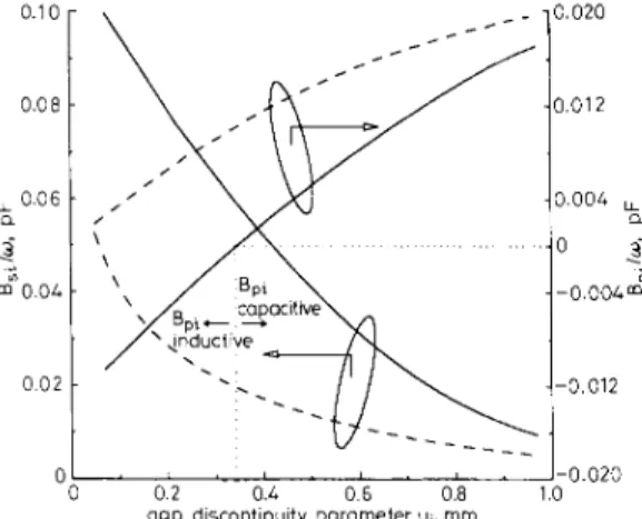
The validity check established in the Section 2.3 allows us to design the gapcoupled filter illustrated in Fig. 1. This section will describe the filter design procedure for an experimental prototype, which incorporates both 90"- bent gap-coupled resonators, assuming 1,4~ = 90", ti = 0.254 mm, and the colinear end-coupled resonators, assuming $i = 0", ti = 0.0 mm (see Fig. 2a). This implies that our prototype will have certain adjacent resonators placed perpendicular to each other. The 0.254 mm thick RT-5880 Duroid substrate of E, = 2.2 is used. Fig. 6 plots the n-circuit discontinuity parameters of the 90"-bent gap-coupled (colinear end-coupled) resonators, under solid (broken) lines, against the gap discontinuity param- eter U , , where vi is assumed to be ui or -u,(O.Omm). When u i is smaller than one-half resonator width (W/2), the adjacent 90"-bent gap-coupled reonators overlap each other, and the overlapping region is square in shape. When ui is greater than W/2, there is no overlapping region defined. Instead, the shortest distance of two adjacent resonators projected into the x-y plane is J(2)(ui - W/2). When the coupling between the reson- ators is strong, or ui < 0.34 mm for the case of 90"-bent gap-coupled resonators, the parallel susceptance Bpi becomes inductive. The change-over phenomenon was also observed and reported by Jansen [23] for the asym- metric series gap-coupled microstrips and SSSs. Note that, prior to obtaining the data shown in the solid line, the convergence study must be performed. The results showed that the least number of terms for P and Q is six to have the converged solution for the capacitance matrix in the present case study. The data shown in both solid 38 1
and broken lines will be further used by the filter synthe- sis equations described in the following section to estab- lish two look-up tables for designing an experimental filter. 0.10 - 0.08 - 0 0 2
1
0.020 0.01 2I
1
-0.012 -0.020 0 0.2 0.L 0.6 0.8 1.0gap discontinuity parameter U,. mm
Fig. 6 Series circuit elements ( 8 , j w ) and parallel circuit elements
(B,,'w) of the equicalent n-circuit of the gap-coupled discontinuities a s functions of the gap discontinuity parameter U,
Structural parameters are (I = 30 mm. b = 30 mm: h , = h , = 0.6 mm; h, =
0 2 5 4 m m ; ~ , = ~ , = I . O , ~ , = 2 2 . I , = 1 2 = 5 . 0 m m : a n d W = 1.84mm Thecal- d a t e d results are obtained under M = N = 5000, and P = 6, Q = 6 for the 90"- bent gapsoupled discontinuity, P = 6, Q = 3 for the colinear end-coupled resonators
~~~~ Colinear end-coupled discontinuity 11, = 0, U , = 0, 4, = 0 )
~ 90 -bent gapcoupled discontinuity ( I , = 0 254 mm, c, = U. or U,, 4, =
90)
3 Design for an experimental K-band gap-coupled bandpass filter
3.1 Filter synthesis equations using admittance inverter [76]
As the experimental filter prototype to be developed is a bandpass filter with less than 20% fractional bandwidth, the filter synthesis based on admittance inverters [16] will provide sufficient accuracy for the specified filter characteristics. For the sake of clarity, the following out- lines the filter synthesis procedure already reported in Reference 16. The filter synthesis begins with the follow- ing expressions:
where 0 and m' represent the angular frequencies in the bandpass and the lowpass domains, respectively, and coo, w 1 and w 2 are the given midband, lower and upper cutoff angular frequencies of the bandpass filter, respectively. 0: is the cutoff angular frequency of the lowpass proto- type, and w is the fractional bandwidth of the bandpass filter. Given the bandpass filter response of E dB, equal ripple in the passband and the filter degree of n, the cor- responding normalised elements' values g , , i = 1, 2,
.. .
, n, of the lowpass prototype can be obtained either by the use of Table 4.05-2 or eqn. 4.05-2 in Reference 16.given by J o , I/YO = J C ~ W / ( 2 ~ 0 ~ l 4 ) 1 J i , i + JYo = nw/C2w;J(gigi+,)I J","+I/YO = JCnw/(2g,g,+,o;)l (164 ( 1 6 4 ( 1 6 4
where go and g n + l are the generator and load imped- ances of the lowpass prototype, respectively. Yo is the normalised admittance of the bandpass filter. Once the above parameters of the admittance inverters are deter- mined, one can design the physical layout for the proto- type filter using the discontinuity parameters reported in Section 2.4. The ideal admittance inverter is approx- imated by the equivalent n-circuit of the gap-coupled dis- continuities in series with two transmission lines with electrical length
mi,
i + as shown in Figs. 7. Applying thefollowing two exprs. 17 and 18, based on the data shown in Fig. 6, two look-up tables are generated and shown in
<---I
?.,
\\
01 " " " " '
0 0.2 0.4 0.6 0.8 1.0
gop discontinuity parameter u i , mm
Fig. 7 8
coupling structures oJFig. 6 against the gap discontinuity parameter U, ~~~~
~ ~~ ~ 90-1
Admittance inverter parameter J,,,, I JY, corresponding 10 the Colinear end-coupled discontinuity (t, = 0. v , = 0, 4, = 0)
90"-bent gap-coupled discontinuity (1, = 0.254 mm, U, = U , or - U , , 4, =
n,
-10 -
1-31 67
<
- 5 0 " " " " " ' I
gap discontinuity parameter ui. m m
0 0.2 0.4 0.6 0.8 1 .o
Fig. 7 8
coupling structures oJFig. 6 against the gap discontinuity parameter U,
Figs. 7A and B for the admittance parameters J i , i + l / Y o and the electrical line length i + respectively.
J i , i + l / y O = Itan CQi,i+1/2
+
tan-l(Bpi/yo)lt
(17)- tan- '(BpJYo) (18)
= - tan-'(2B,JYo
+
BpJYo)where BSi and Bpi are evaluated at midband frequency
fo = 21.494 GHz, and Yo is normalised at 0.02. The value of computed from eqn. 18 is negative for most gap-coupled discontinuities. These negative electrical lengths @ i - l . i and Q j i . j + l are absorbed into the ith half- wavelength SSS resonator. The electrical length of this resonator becomes
ei
= 180"+
(mi-
1,+
q,
~2 (19)The use of the look-up tables illustrated by Figs. 7A and B will be explained by the following filter prototype design example.
3 2 Experimental bandpass filter design
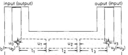
Fig. 8 shows the circuit layout of the experimental bandpass prototype employing both 90"-bent gap- coupled resonators and colinear end-coupled resonators.
input (output)
m
ouput (input)m
I 1 I '
' I I I
Fig. 8 Circuit layout of experimental three-resonator gap-coupled S S S bandpass filter
Resonators with solid lines are on the top surface of the substrate, and those with broken lines are on the bottom side of the substrate. The gap discontinuity parameters U,, i = 0, I , 2, 3 and the physical length of the resonators I,, L = I , 2, 3, will be determined by the use of Figs. 7A and B
Such an implementation, using various types of coupling structure, results in the input and output ports being located at the same reference plane, which in turn results in zero compressed length for the filter. The 90"-bent gap- coupled discontinuities are at both the lower left and the lower right corners of the circuit layout, where the input and output ports are connected to the top SSSs, shown in solid lines. The first, second and third resonators are underneath the substrate and are perpendicular to the input and output SSSs. The first (second) and second (third) resonators are arranged in the colinear end- coupled fashion.
Given the specifications that assume 0.2 dB equal ripple passband loss between 21 and 22GHz and the filter degree of three, as already implied in Fig. 8, one may obtain the parameter values of the admittance inverter by using eqns. 160-c. Once those values have been obtained, the gap discontinuity parameters u i , i = 0, I, 2, 3 and the physical length of the resonators I , , i = I, 2, 3, as shown in Fig. 8, are determined by the use of Figs. 7A and B. For example, starting with the admit- tance inverter parameter of 0.24 for the 90"-bent gap- coupled resonators, one can follow the arrow symbols shown in Fig. 7A to determine the value of the gap dis- continuity parameter uo (or ug). Starting from this value uo(u,), which is 0.52 mm in this particular case, one can follow the arrow symbols again to determine the value of
IEE PROCEEDINGS-H, Vol. 139, No. 4 , A U G U S T 1992
Qi, i + I in Fig. 7B. Once all the values of Qi, i + for i = 0,
1, 2, 3 are obtained, the electrical length of the three res- onators are determined by eqn. 19. Therefore the design is completed by knowing all the gap discontinuity param- eter u i , i = 0, 1, 2, 3 and the electrical length O i , i = I, 2, 3.
4 Comparison between theoretic and
Fig. 9 is a photograph of the experimental filter together with the structural parameters corresponding to Fig. 2a
experimental results
Fig. 9 Photograph of a 21-22 GHz three-resonator gap-coupled S S S bandpass filter prototype placed in a 1.454 m m high and 4 m m wide rec- tangular waveguide housing
Structural parameters corresponding to Fig. 2A and Fig. 8 are h , = h, = 0.6 m m ; h , = 0.254 m m , c l = E~ = 1.0; c2 = 2 2 : W = 1.84 m m : I, = I , = 5.52 m m ; I, =
5 73 m m , vo =
-0.52mm,r~,=052mm,r,~r,=0.0mm:~,=~,=O":u,=u,=0.65mm: c , = ~ ~ = O O m m
t o = I, = 0.254 m m : @, = @, = 90"; uo = U, = 0.52 m m ,
and Fig. 8. The SSS resonators on the 0.254" thick RT-5880 Duroid substrate are placed symmetrically in a 1.454 mm high and 4 mm wide rectangular waveguide housing. All the resonators have the same 50
R
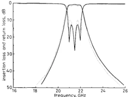
charac- teristic impedance. It is found that, under these design parameters, the SSS has the cutoff frequency of the first higher-order mode at about 36GHz [21], which is far beyond our stopband frequency of interest in our proto- type design.Fig. 10 superimposes the plots for the measured filter responses and the theoretic predictions for the insertion
loss and the return loss of a zero compressed length, 21- 22 GHz three-resonator gap-coupled bandpass filter prototype, respectively. The theoretic results are obtained by the TouchstoneTM microwave circuit simulation, pro- vided with the discontinuity parameters B,Jw and B,Jw,
i = 0, 1, 2, 3 and the complex propagation constants accounting for the lossy SSSs with various physical lengths l i , i = 1, 2, 3. The complex propagation constant (a.
+
j p ) for the SSS at 21.494 GHz was found to be =1.0846k0 and tl = 5.57 x dB/mm, based on the rig- orous full-wave mode-matching program [24] assuming
I O pm thick copper strip with conductivity
U = 5.85 x IO' (Sjm). The measured filter responses show less than 1.4 dB insertion loss and greater than IO dB return loss in the passband.
The filter was constructed by a typical hybrid micro- wave integrated circuit (MIC) photolithography process which has 0.02 mm resolution tolerance. Neither tuning nor layout compensation of any kind was conducted. In 383
Fig. 10, both measured and theoretic filter responses are in excellent agreement. This also confirms the accuracy of our de-embedding procedure for the gap-coupled discon- tinuities described in Section 2.
18 20 2 2 24 26
f r e q u e n c y , GHz
Fig. 10 Theoretic and measured filter responses of a 21-22 GH: three-resonator gap-coupled SSS bandpassfilter prototype
_____ Theoretic filter responses
. . . Measured filter responses
5 0 1 6 ’ ” ” ” ”
’
5 Conclusions
A new gap-coupled SSS bandpass filter design is pre- sented in detail. The new filter configuration can orient the resonators in any arbitrary direction. This makes the new filter highly flexible to interface with other micro- wave circuit components and eliminates all possible forms of interference among them.
The fact that the SSS gap-coupled resonators are very complicated in shape and possess no symmetry mandates an accurate and efficient de-embedding algorithm to determine the equivalent n-circuit parameters of the gap- coupled discontinuity problem for carrying out the filter synthesis. A de-embedding procedure described in Section 2, employing the three-dimensional quasi-TEM SDA incorporating a new set of basis functions, was validated by the data existing in the literature.
The design procedure described, which involves two look-up tables, enables the physical layout of the gap- coupled filter to be determined very quickly, although the filter is complicated in shape. A 21-22GHz zero com- pressed length bandpass filter, consisting of both 90”-bent gap-coupled resonators and colinear end-coupled reson- ators, was built and tested. Both measured and predicted filter responses agree very well in both passband and stopband. The constructed filter is the first-pass design requiring neither tuning nor adjustment. Thus, the filter design technique presented here is proved to be suitable for the MIC process, which makes it cost-effective and reproducible.
384
6 References
1 RHODES, J.D.: ‘Suspended substrate filters and multiplexers’. Pro- ceedings of 1986 European Microwave Conference, 16th EuMc, pp. 8-18
2 DEAN, J.E.: ‘Suspended substrate stripline filters for ESM applica- tions’, IEE Proc. F , Commun., Radar & Signal Process, 1985, 132, (4), pp. 257-266
3 DEAN, J.E.: ‘Microwave integrated circuit broadband filters and continguous multiplexers’. PhD thesis, University of Leeds, 1979 4 MOBBS, C.I., and RHODES, J.D.: ‘A generalized Chebyshev sus-
pended substrate stripline bandpass filter’, IEEE Trans., 1983,
M l T - 3 1 , (9, pp. 397-402
5 LOSCH, I.E., and MALHERBE, J.A.G.: ‘Design procedure for inhomogeneous coupled line sections’, IEEE Trans., 1988, MIT-36, (7). pp. 1186-1190
6 LEVY, R.: ‘New equivalent circuits for inhomogeneous coupled lines with synthesis applications’, IEEE Trans., 1988, MIT-36, (6), pp. 1087-1094
7 RUBIN, D., and HISLOP, A.R.: ‘Millimeter-wave coupled line filters’, Microw. J., 1980, 23, pp. 67-78
8 TON, T.N., SHIH, Y.C., and BUI, L.Q.: ‘18-30GHz broadband bandpass harmonic reject filter’. Digest of 1987 lEEE MTT-S Inter- national Microwave Symposium, Session J-37, pp. 387-389 9 NGUYEN, C., and CHANG, K.: ‘Design and performance of
millimeter-wave end-coupled bandpass filters’, Int. J . Infrared & Millim. Waves, 1985,6, (7), pp. 497-509
IO DOUGHERTY, R.M.: ‘MM-wave filter design with suspended stripline’, Microw. J . 1986, 29, pp. 75-84
11 TZUANG, C.-K.C., CHIANG, Y-C., and SU, S.: ‘Design of a quasi- planar broadside end-coupled bandpass filter’. Digest of 1990 IEEE MTT-S International Microwave Symposium, Session 1-36, pp. 407- 410
12 ZYSMAN, G.I., and JOHNSON, A.K.: ’Coupled transmission line networks in an inhomogeneous dielectric medium’, IEEE Trans., 1969, MTT-17, (lo), pp. 753-759
13 RHODES, J.D.: ‘Design formulas for stepped impedance distributed and digital wave maximally flat and Chebysbev low-pass prototype filters’, IEEE Trans., 1975, CAS-22, (1 l), pp. 866-874
14 ITOH, T.: ‘Generalized spectral domain method for multiconductor printed lines and its application to turnable suspended microstrips’, IEEE Trans., 1978, MTT-26, (U), pp. 983-987
15 NAGHED, M., and WOLFF, I.: ‘Equivalent capacitances of copla- nar waveguide discontinuities and interdigitated capacitors using a three-dimensional finite difference method‘, IEEE Trans., 1990, MTT-38, (12), pp. 1808-1815
16 MATTHAEI, G.L., YOUNG, L., and JONES, E.M.T.: ‘Microwave filters, tmpedance-matching networks, and coupling structures’ (McGraw Hill, New York, 1964), Chaps. 8 and 4
17 ITOH, T., MITTRA, R., and WARD, R.D.: ‘A method for comput- ing edge capacitance of finite and semi-infinite microstrip lines’, IEEE Trans., 1972, MTT-20, (12), pp. 847-849
18 COLLIN, R.E.: ‘Field theory of guided waves’ (The Institute of Electrical and Electronics Engineers, Inc., New York 1991), p. 278 19 JANSEN, R.H.: ‘The spectral-domain approach for microwave
integrated circuits’ IEEE Trans., 1985, MTT-33, (lo), pp. 1043-1056 20 TZUANG, C.-K.C., and KUO, J.-T.: ‘Modal current distribution on
closely coupled microstrip lines: a comparative study of the SDA basis functions’, Electron. Lett., 1990, 26, (7), pp. 464-465 21 KUO, J.-T., and TZUANG, C.-K.C.: ‘Complex modes in shielded
suspended coupled microstrip lines’, IEEE Trans., 1990, MIT-38, (9), pp. 1278-1286
22 UWANO, T.: ‘Accurate charactenzation of microstrip resonator open end with new current expression in spectral-domain approach, IEEE Trans., 1989, MTT-37, (3), pp. 630-633
23 KOSTER, N.H.L., and JANSEN, R.H.: ‘The equivalent circuit of the asymmetrical series gap in microstrip and suspended substrate lines’, IEEE Trans., 1982, MTT-30, (8), pp. 1273-1279
24 TZUANG, C.-K. C., CHEN, C.-D., and PENG, S.-T.: ‘Full-wave analysis of lossy quasi-planar transmission line incorporating the metal modes’, IEEE Trans., 1990, m - 3 8 , (12), pp. 1792-1799