Crystal Quality of 3C-SiC Influenced by the Diffusion Step
in the Modified Four-Step Method
Wei-Yu Chen,a Wei-Lin Wang,c Jui-Min Liu,a Chien-Cheng Chen,a Jenn-Chang Hwang,a,zChih-Fang Huang,band Li Changc
a
Department of Materials Science and Engineering and bDepartment of Electrical Engineering, National Tsing Hua University, Hsinchu City 30013, Taiwan
c
Department of Materials Science and Engineering, National Chiao Tung University, Hsinchu City 30013, Taiwan
The atomic arrangement and bonding characteristics of void-free 3C-SiC/Si共100兲 grown by the modified four-step method are presented. Without the diffusion step, Si–C bonds are partially formed in the as-carburized layer on Si共100兲. The ratio of C–C bonds to Si–C bonds is about 7:3, which can be lowered to about 1:9 after the diffusion step at 1350°C for 5 min or at 1300°C for 7 min according to C 1s core level spectra. The residual C–C bonds cannot be removed, which is associated with an irregular atomic arrangement共amorphous兲 located either at the 3C-SiC/Si共100兲 interface or at the intersection of twin boundaries in the 3C-SiC buffer layer based on the lattice image taken by transmission electron microscope. The diffusion step helps the formation of Si–C bonds more completely and results in a SiC buffer layer of high quality formed on Si共100兲 before the growth step. However, twins and stacking faults still appear in the 3C-SiC buffer layer after the diffusion step. The formation mechanism of the 3C-SiC buffer layer is proposed and discussed.
© 2010 The Electrochemical Society. 关DOI: 10.1149/1.3294700兴 All rights reserved.
Manuscript submitted September 11, 2009; revised manuscript received December 11, 2009. Published February 4, 2010.
Silicon carbide共SiC兲 is a wide bandgap semiconductor for high power and high frequency devices due to its excellent thermal and electrical characteristics.1,2 Single-crystalline SiC in 4H and 6H polytypes is expensive and commercially available for device fabrication.3,4As a means to lower the production cost, the het-eroepitaxy of 3C-SiC on Si has attracted attention in the past de-cades. The difficulty to grow a 3C-SiC layer of good quality on Si arises from large lattice mismatch共⬃20%兲 and difference in ther-mal expansion coefficients共⬃8%兲. The breakthrough in the growth of 3C-SiC on Si using a buffer layer was first reported by Nishino et al.5A conventional three-step method, consisting of cleaning, car-burization, and growth, was proposed and illustrated.5The carbur-ization step plays two roles in the growth of 3C-SiC on Si in the conventional three-step method. One is to supply carbon atoms in the form of amorphous carbon onto Si at carburization temperature, usually at 1250°C for the C3H8/H2/SiH4 system. The other is to
form a 3C-SiC buffer layer by driving Si atoms out of the Si sub-strate into the amorphous carbon layer at carburization temperature. The carburization step has become a standard procedure for the growth of 3C-SiC on Si since then.6-11 However, voids6-9,12-16and micropipes,17,18which are attributed to the out-diffusion of Si at-oms, appear at the 3C-SiC/Si interface after carburization. In addi-tion to voids and micropipes, planar defects such as twins and stack-ing faults are generated in the 3C-SiC buffer layer as a result of the strain relaxation at the lattice-mismatched SiC/Si interface. The pla-nar defects are generated and propagated along the兵111其 planes in 3C-SiC grown on Si, which usually occurs at a high heating rate and a low partial gas pressure of carbon, reported by Cimalla et al. and Yun et al.19,20
The conventional three-step method is a long time process cause it requires cooling the samples back to room temperature be-tween each step. It takes about 1 h to cool the sample from process temperature to room temperature in each step. The conventional three-step method can be performed either by atmospheric pressure chemical vapor deposition共APCVD兲 or by low pressure chemical vapor deposition共LPCVD兲. Zorman et al. showed in 1995 that the void-free growth of 3C-SiC films on a large area of Si substrates was achieved by APCVD using the conventional three-step process.21However, two major issues associated with the LPCVD growth of 3C-SiC epitaxial films using the conventional three-step method remain to be solved. One is the voids at the SiC/Si interface
because the out-diffusion of Si atoms is severe in LPCVD. The other is the planar defects 共twins and stacking faults兲 generated in the 3C-SiC buffer layer due to the lattice-mismatch-induced stress at the SiC/Si interface.
In 2008, Chen et al. developed the modified four-step method 共cleaning, carburization, diffusion, and growth兲 associated with the LPCVD growth by inserting a diffusion step and by removing the cooling step in the conventional three-step method.22The modified four-step method can be performed in a shorter time than the con-ventional three-step method because the cooling process between each step is removed. A void-free 3C-SiC film of high quality can be grown on Si共100兲 in a mixed gas of SiH4–C3H8–H2using LPCVD.
The quality of the 3C-SiC buffer layer is improved by introducing the diffusion step in the modified four-step method reported in our previous work.22The major role of the diffusion step is to assist the Si–C bond formation more efficiently by decoupling the out-diffusion of Si atoms from the deposition of amorphous carbon. However, the atomic arrangement and bonding characteristics of the 3C-SiC buffer layer are unclear.
In this paper, we present the variation in structural and bonding characteristics of the 3C-SiC buffer layer grown on Si共100兲 by LPCVD at different diffusion temperatures and times. The formation mechanism of the 3C-SiC buffer layer is also proposed to explain the growth of high quality 3C-SiC on Si共100兲 by the modified four-step method according to the structural and bonding information.
Experimental
A horizontal cold-wall-type LPCVD system with induction heat-ing was used for the growth of 3C-SiC on a p-type Si共100兲 substrate, which was illustrated previously by other groups.23The Si共100兲 sub-strate of 1⫻ 1 cm was dipped in 1% HF for 30 s, rinsed by deion-ized water, and then placed on a SiC-coated graphite susceptor that was heated by radio-frequency induction. The mixed gas of SiH4 共5% in H2兲 and C3H8共4N兲 was carried by H2共5N兲 into the LPCVD
chamber for the growth of 3C-SiC on Si共100兲. The temperature was ramped up at a rate of about 11°C/s and measured by a thermo-couple and an IR pyrometer. The total pressure was varied by con-trolling the throttle valve between the LPCVD chamber and the mechanical pump. Most samples were treated with the modified four-step method shown in Fig.1a. Some samples were treated with the modified four-step method without the growth step shown in Fig. 1bfor comparison.
The optimum experimental parameters for the modified four-step method listed in TableIwere reported in our previous work.22The growth rate of 3C-SiC was approximately 3 m/h, and all the
3C-z
E-mail: jch@mx.nthu.edu.tw
Journal of The Electrochemical Society, 157共3兲 H377-H380 共2010兲
0013-4651/2010/157共3兲/H377/4/$28.00 © The Electrochemical Society H377
) unless CC License in place (see abstract). ecsdl.org/site/terms_use
address. Redistribution subject to ECS terms of use (see 140.113.38.11
SiC film thicknesses were kept at 1.5 m in this study. The struc-tural information of 3C-SiC films was characterized using a Rigaku D/MAX2000 X-ray diffractometer共XRD兲 with a Cu K␣ radiation 共1.5405 Å兲 and an FEI TECNAI G2 transmission electron micro-scope 共TEM兲. The bonding characteristics of 3C-SiC films were characterized using X-ray photoelectron spectroscopy 共XPS, PHI ESCA 1600兲.
Results and Discussion
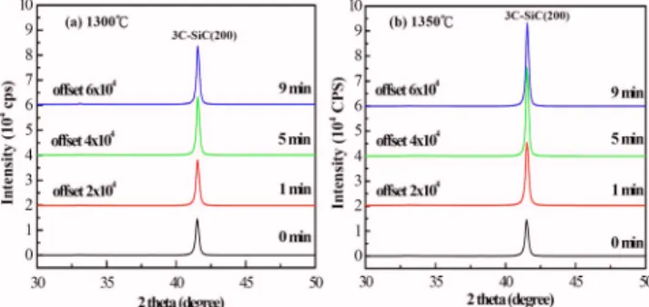
The crystal qualities of 3C-SiC films grown on Si共100兲 using the modified four-step method are strongly affected by temperature and process time at the diffusion step, as shown in the XRD spectra in Fig.2aandb. Only the共200兲 peak of 3C-SiC appears in each XRD spectrum, indicating that the as-grown 3C-SiC film is either highly oriented or epitaxial. The共200兲 peak of 3C-SiC increases in inten-sity with process time at 1300°C, as shown in Fig.2a. The role of the diffusion step at 1300°C is to assist the growth of 3C-SiC films of good quality before the growth step. When the temperature is raised from 1300 to 1350°C, a higher intensity of 3C-SiC共200兲 can be achieved at a shorter process time. The improvement of the crys-tal qualities of the 3C-SiC films by the diffusion step is also con-firmed by X-ray rocking curve measurements. The full width at half-maximum共fwhm兲 of 3C-SiC共200兲 reduces from 0.77 to 0.73
and from 0.77 to 0.67 by treating samples with the diffusion step at 1300 and 1350°C for 9 min, respectively, as listed in TableII. A better crystal quality of the 3C-SiC film can be obtained within a shorter process time at a higher temperature.
The quality improvement of the SiC buffer layer is further inves-tigated by XPS and TEM for the as-diffused 3C-SiC/Si共100兲 samples 共grown by the modified four-step method without the growth step in our LPCVD system兲. The Si–C bond formation of the as-diffused 3C-SiC/Si共100兲 samples is clearly illustrated by the curve-fit of the C 1s core level spectra in Fig.3a and b. All the Si共100兲 samples are carburized at a C3H8 partial pressure of 1.9
⫻ 10−2 Torr and at 1250°C for 1.5 min before treating with the
diffusion step at 1300 or 1350°C. There exists a broad shoulder共or peak兲 on the left side of the prominent C 1s peak at ⬃283 eV, indicating the existence of two types of carbon bonding environ-ments in the 3C-SiC buffer layer after diffusion. The two C 1s components located at 284.5 and 283.2 eV are required to obtain consistent curve-fit results, which are assigned as C–C and Si–C bonds, respectively. The difference in the C 1s binding energies of the C–C and Si–C bonds results from the different amounts of charge transfer. The corresponding curve-fit results are also listed in TableII. The ratio of Si–C bonds to C–C bonds for the as-carburized 3C-SiC/Si共100兲 sample is about 3:7, suggesting that Si–C bonds form partially at the carburization step. In other words, the Si atoms diffused out of Si共100兲 are not enough to transform the as-carburized layer into SiC and result in excess carbon共C–C bonds兲 that resided in the as-carburized Si共100兲 layer. The excess carbon Figure 1. Schematic showing the processes for the growth of 3C-SiC on Si.
共a兲 The modified four-step method. 共b兲 The modified four-step method with-out the growth step.
Table I. Optimal experimental parameters at each step in the modified four-step method.
Clean Carburization Diffusion Growth
H2共sccm兲 1000 1000 1000 1000
C3H8共sccm兲 0 10 0 3
SiH4共sccm兲 0 0 0 20
Temperature共°C兲 900 1250 1350 1420
Pressure共Torr兲 10 2 2 0.8
Figure 2.共Color online兲 XRD spectra of the 3C-SiC films grown on Si共100兲
by the modified four-step method at different diffusion conditions:共a兲 1300 and共b兲 1350°C.
Table II. FWHM of the SiC(200) peak and the area percentages of the C–C and C–Si bonds deconvoluted from C 1s core level spectra taken from the samples treated with different diffusion conditions (temperature and process time).
Diffusion temperature
共°C兲 Diffusion time共min兲 fwhm共°兲 C–C共%兲 C–Si共%兲
1300 0 0.77 69a 31a 1 0.76 48 52 3 — 27 73 5 0.74 19 81 7 — 8 92 9 0.73 8 92 1350 0 0.77 69a 31a 1 0.71 36 64 3 — 19 81 5 0.67 10 90 7 — 8 92 9 0.67 7 93
aData extracted from the C 1s core level spectra for the sample
with-out the diffusion treatment.22
H378 Journal of The Electrochemical Society, 157共3兲 H377-H380 共2010兲
H378
) unless CC License in place (see abstract). ecsdl.org/site/terms_use
address. Redistribution subject to ECS terms of use (see 140.113.38.11
results from the carbon deposition at a high C3H8 flow rate 共10
sccm兲 that is designed to cover the Si共100兲 surface quickly to avoid the interfacial void formation at the carburization step. The as-carburized Si共100兲 surface with excess carbon can be further trans-formed into a SiC buffer layer at the diffusion step before the growth step. After diffusion at 1300°C, the amount of Si–C bonds increases with process time and reaches a maximum value at approximately 7 min, accompanied with the reduction in C–C bonds. The highest ratio of Si–C bonds to C–C bonds is about 9:1. The⬃10% excess carbon共C–C bonds兲 still resides in the SiC buffer layer, which is probably located at the intersection of twins that are illustrated in TEM micrographs and discussed later. A similar result occurs at a faster rate for the diffusion step at 1350°C. The relative amount of Si–C bonds increases with process time and reaches a maximum value at approximately 5 min, as indicated in TableII. The faster increase rate of Si–C bonds at 1350°C indicates that the Si–C bond formation in the SiC buffer layer is controlled by a diffusion-limited process. The Si–C bond formation in the SiC buffer layer enables the growth of a SiC film of better quality at the growth step, sup-ported by the higher intensity of 3C-SiC共200兲 shown in Fig.2aand band by the smaller fwhm of the corresponding XRD rocking curve listed in TableII.
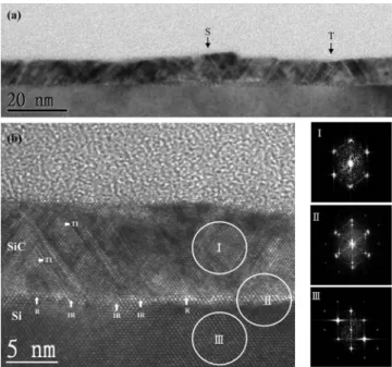
The structural information of the SiC buffer layer is further char-acterized by using high resolution transmission electron microscopy 共HRTEM兲. Figure 4a shows the bright-field cross-sectional TEM micrograph of the as-diffused sample treated at 1350°C for 9 min. An ultrathin SiC layer of⬃10 nm thick is stacked on Si共100兲 with a surface roughness of less than 1 nm. Several twins and stacking faults are identified and marked with “T” and “S,” respectively. The atomic arrangement at the 3C-SiC/Si共100兲 interface is revealed in the HRTEM lattice image in Fig.4b. Many planar defects, including twins and stack faults, are inclined on兵111其 planes of 3C-SiC near the 3C-SiC/Si共100兲 interface. The generation of twins and stacking faults is attributed to high heating rate and low C3H8partial pres-sure, according to previous publications.19,20 The propagation of twins stops when two inclined twins intersect, reported by Yagi and Nagasawa.24The atomic arrangement at the intersection of twins, marked with “TI,” is irregular共amorphous兲 in the lattice image in Fig.4b. The excess carbon共C–C bonds兲 is probably located at the TI locations. The具111典 directions in the lattice image of the 3C-SiC buffer layer in Fig.4b are not straight, indicating that the 3C-SiC crystal is distorted due to the lattice-mismatch-induced stress at the 3C-SiC/Si共100兲 interface. Moreover, the ⬃0.7 nm thick interface is not uniform, which is blended with regular共R兲 and irregular atomic arrangements. The excess carbon共C–C bonds兲 is probably located at
the irregular locations. Three fast Fourier transform共FFT兲 images, taken from three small regions circled in the lattice image共I, II, and III兲, are placed in Fig. 4b, next to the HRTEM lattice image. The FFT image I with clear spots is identified to be the electron diffrac-tion共ED兲 pattern of 3C-SiC looking from the zone axis 关110兴, indi-cating the good crystalline quality of 3C-SiC. The FFT image II, taken from the interface, is identified to be a combination of Si and 3C-SiC ED patterns. Both Si and 3C-SiC are in an epitaxial orien-tation relationship. The FFT image III with sharp spots is deter-mined to be the ED pattern of Si. The three FFT images and the lattice image in Fig.4bsupport that the ultrathin SiC buffer layer is single crystalline. However, some planar defects and irregular atomic arrangements exist in the 3C-SiC buffer layer.
The formation of the SiC buffer layer at carburization and diffu-sion steps is proposed and described as follows: First, the amor-phous carbon is deposited on Si共100兲 and partially reacted with Si atoms to form Si–C bonds when a high flow rate共10 sccm兲 of C3H8
is introduced into the LPCVD chamber at the carburization step. The ratio of C–C bonds to Si–C bonds is about 7:3, right after the car-burization step, according to the XPS data. There should be a SiC nuclei dispersed in a matrix of amorphous carbon after the carbur-ization step because the volume ratio of C–C bonds is very large共 ⬃70%兲. Second, the diffusion step assists in the Si–C bond forma-tion more completely. The TEM image indicates that the SiC layer is finally in a crystal form on Si共100兲 after the diffusion step. This supports the fact that SiC nuclei grow in size by forming Si–C bonds via the out-diffusion of Si atoms toward the amorphous carbon layer. The out-diffusion of Si atoms stops, and the ratio of the C–C bonds to the Si–C bonds reaches⬃1:9 after the diffusion step. A continu-ous SiC buffer layer is finally formed on Si共100兲. The residual C–C bonds are probably associated with irregular atomic arrangements, which are located either at the 3C-SiC/Si共100兲 interface or at the intersection of twin boundaries shown in the TEM lattice image in Fig.4b.
Conclusions
A void-free 3C-SiC/Si共100兲 interface can be achieved by LPCVD using the modified four-step method. The formation of Si–C bonds is not sufficient at the carburization step. The 3C-SiC nuclei are dispersed in a matrix of amorphous carbon after the car-Figure 3. C 1s core level spectra of the as-diffused 3C-SiC/Si共100兲 samples
as a function of temperature and process time:共a兲 1300 and 共b兲 1350°C. The curve-fit results are marked with C–C and C–Si to represent their corre-sponding bonding components.
Figure 4. Cross-sectional view TEM micrographs taken at the SiC/Si共100兲
interface.共a兲 Bright-field TEM image. 共b兲 HRTEM lattice image. Three dif-ferent regions共I, II, and III兲 are circled to obtain the FFT images 共equivalent to ED patterns兲.
H379
Journal of The Electrochemical Society, 157共3兲 H377-H380 共2010兲 H379
) unless CC License in place (see abstract). ecsdl.org/site/terms_use
address. Redistribution subject to ECS terms of use (see 140.113.38.11
burization step. The diffusion step helps the formation of Si–C bonds more completely before the growth of 3C-SiC. A 3C-SiC buffer layer of high quality is formed on Si共100兲 after the diffusion step. However, twins and stacking faults, resulting from the relax-ation of strain, cannot be removed after the diffusion step.
Acknowledgment
The work is sponsored by the National Science Council through the project NSC96-2218-E-007-003.
National Tsing Hua University assisted in meeting the publication costs of this article.
References
1. C. M. Zettetling, Process Technology for Silicon Carbide Device, p. 4, Institution of Electrical Engineers, London共2002兲.
2. J. B. Casady and R. W. Johnson, Solid-State Electron., 39, 1409共1996兲. 3. J. W. Palmour, J. A. Edmonda, H. S. Konga, and C. H. Carter, Physica B, 185, 461
共1993兲.
4. C. E. Weitzel, J. W. Palmour, C. H. Carter, K. Moore, K. J. Nordquist, S. Allen, C. Thero, and M. Bhatnagar, IEEE Trans. Electron Devices, 43, 1732共1996兲. 5. S. Nishino, J. A. Powell, and H. A. Hill, Appl. Phys. Lett., 42, 460共1983兲. 6. A. J. Steckl and J. P. Li, IEEE Trans. Electron Devices, 39, 64共1992兲. 7. P. Liaw and R. F. Davis, J. Electrochem. Soc., 132, 642共1985兲.
8. J. A. Powell, L. G. Matus, and M. A. Kuczmarsk, J. Electrochem. Soc., 134, 1558 共1987兲.
9. J. D. Hwang, Y. K. Fang, Y. U. Song, and D. N. Yaung, Jpn. J. Appl. Phys., Part 1, 34, 1447共1995兲.
10. K. Ikoma, M. Yamanaka, H. Yamaguchi, and Y. Shich, J. Electrochem. Soc., 138, 3028共1991兲.
11. H. Nagasawa, K. Yagi, and T. Kawahara, J. Cryst. Growth, 237–239, 1244共2002兲. 12. H. J. Kim, R. F. Davis, X. B. Cox, and R. W. Linton, J. Electrochem. Soc., 134,
2269共1987兲.
13. C. C. Chiu and S. B. Desu, J. Mater. Res., 8, 535共1993兲. 14. J. P. Li and A. J. Steckl, J. Electrochem. Soc., 142, 634共1995兲.
15. G. Ferro, Y. Monteil, H. Vincent, V. Thevenot, M. D. Tran, F. Cauwet, and J. Bouix, J. Appl. Phys., 80, 4691共1996兲.
16. A. Severino, G. D’Arrigo, C. Bongiorno, S. Scalese, F. La Via, and G. Foti, J. Appl. Phys., 102, 023518共2007兲.
17. R. Scholz, U. Gösele, E. Niemann, and D. Leidich, Appl. Phys. Lett., 67, 1453 共1995兲.
18. R. Scholz, U. Gösele, E. Niemann, and F. Wischmeyer, Appl. Phys. A: Mater. Sci. Process., 64, 115共1997兲.
19. V. Cimalla, Th. Stauden, G. Eichhorn, and J. Pezoldt, Mater. Sci. Eng., B, 61–62, 553共1999兲.
20. J. Yun, T. Takahashi, T. Mitani, Y. Ishida, and H. Okumura, J. Cryst. Growth, 291, 148共2006兲.
21. C. A. Zorman, A. J. Fleischman, A. S. Dewa, M. Mehregany, C. Jacob, S. Nishino, and P. Pirouz, J. Appl. Phys., 78, 5136共1995兲.
22. W. Y. Chen, C. C. Chen, J. Hwang, and C. F. Huang, Cryst. Growth Des., 9, 2616 共2009兲.
23. S. Nishino, Y. Hazuki, H. Matsunami, and T. Tanaka, J. Electrochem. Soc., 127, 2674共1980兲.
24. K. Yagi and H. Nagasawa, Mater. Sci. Forum, 264–268, 191共1998兲.
H380 Journal of The Electrochemical Society, 157共3兲 H377-H380 共2010兲
H380
) unless CC License in place (see abstract). ecsdl.org/site/terms_use
address. Redistribution subject to ECS terms of use (see 140.113.38.11