INTERNATIONAL JOURNAL OF CIRCUIT THEORY AND APPLICATIONS, VOL. 17, 447-464 (1989)
A NEW GENERAL
METHOD
TO MODEL SIGNAL TIMING
OF
E/D
NMOS LOGIC
CHUNG-YU WCJ AND YEN-TAI LINDepariiiiet71 a,/ Eleclronic Engineering and Insririrle oJ Elecirorircs, Nrriiotial Chiao Tirng Universiiy, 75 Po-Ai Sireel. Hsin-CI~ir
30039 Tuiirvn, Repirhlic of China
SUMMARY
A new general modelling method for E / D NMOS logic i 5 proposed and applied to the case of inverters. In this model,
non-linear device currents in the large-signal equivalent circuit are reformulated by the curve-fitting technique. Then output voltage wave-forms are analytically solved region by region from the equivalent circuit. From the derived formulae, the riselfall time and delay time can be calculated. Wide-range comparisons with SPICE simulation results were performed to verify the accuracy and the general applicability of the developed model. Two examples are given to demonstrate the applications of the developed timing model to timing analysis. I t is shown that the model has a good accuracy for E/D inverters w i t h a wide range of beta ratios, gate sizes, capacitive loads, input voltage wave-forms and device parameters. Moreover, the required CPU time and memory are small. These make the proposed modelling method an interesting approach to model E/D NMOS gates for CAD applications.
1 . INTRODUCTION
As VLSI/ULSl MOS devices are scaled down to increase chip density, circuit complexity and operation speed, circuit design becomes a challenging task to retain the full benefit of scaling down while optimizing performance for a highly complicated circuit. Since signal delay is one of the fundamental characteristics of a digital MOS IC, many valuable approaches' 2') have so far been taken to develop sophisticated timing models or macromodels which can aid the circuit design in many ways. They are:
( I ) to provide a solid base for circuit optimization and automatic s i ~ i n g ~ ~ ~ . ' ~ ~ ' ~ (2) to provide CAD models for efficient timing analysis or verification on complicated VLSI/ULSI
circuits with reasonable speed, computer memory and a c c u r a ~ y ' ~ ~ ~ ' ~ ~ ' ' ~ ' ~ ~ ~ ~
(3) to improve the accuracy of delay calculations in logic simulations""
(4) to provide a deep insight into the speed nature of digital MOS I C S . ~ . ' ~
One interesting approach recently developed
'
" is to derive delicate analytical timing models or macromodels for MOS digital gates using suitable device equations and equivalent circuits. In this approach, some models were specially developed for static CMOS gates2*699"3s'4 or domino CMOS, while others 1 , 3 - 5 , 7 , 1 0 - 12 were developed for E/D NMOS logic gates. Unlike the conventional analytic models intextbooks, they all characterize output responses under non-step input excitations, rather than ideal step input, using different modelling methods.
For E/D NMOS gates, the delay was modelled by considering charging and discharging of capacitive loads"'*'' with averaged currents" or fixed currents, by deriving accurate formulae from SPICE
simulation results I' or the gate transfer curve, or by piecewise linearized circuits. Specifically, the two modelling methods proposed by Simmons and Taylor and Etiemble et a / . are based on the large-signal model with determined device resistances for the characterization of submicrometre oscillators and with simple device equations and linearized device parameters and wave-forms' respectively.
Other approaches for gate delay modelling are RC models which treat transistors as effective
resistors and bounding algorithms which seek upper and lower bounds for output responses of gates 0098-9886/89/040447- 18$09.00
0
1989 by John Wiley & Sons, Ltd.Received I5 April 1988 Revised I September 1988
448 C:Y. W U A N D Y:T. L I N
or interconnects. ' ' - 2 0 Generally, these approaches make a trade-off between speed and accuracy of timing analysis.
All these works are important stages in timing model development. However, i t is found that some key problems still have to be solved to achieve the four goals mentioned above. First, accurate device equations are required in a timing model to improve its accuracy. Secondly, the accuracy has to be definitely verified for a wide range of NMOS device dimensions and parameters. Thirdly, the modelling method has to be applicable to complex NMOS gates. Finally, the predetermined model parameters from either experimental measurements o r fully transient circuit simulations have t o be eliminated so that the model can be applied to optimization o r autosizing. I t is the purpose of this study to develop a new modelling approach for the E / D NMOS logic, which provides a direction to solve the above problem. Before introducing the new models, the inherent difficulty in modelling the E / D NMOS logic will be described.
According to our observations, the modelling work for E / D NMOS logic is far more difficult than that for CMOS, even in the case of a simple inverter. The difficulties originate from:
(1) wide ranges of device beta ratios and sizes which require a high model generality
( 2 ) slower rising wave-forms which increase the latency a n d the initial
(3) faster falling wave-forms which enhance their sensitivities to input rising wave-forms.
We have tried to develop models of E / D NMOS inverters using the same method as in CMOS6*9 and failed t o obtain satisfactory accuracy for inverters with wide ranges of device dimensions and excitation inputs.
The new modelling method to be presented here overcomes the above difficulties partly by using the curve-fitting technique t o accurately calculate the drain currents in transient operations and partly by modelling the initial delay which is related to the device subthreshold characteristics. In the characteristic wave-form case, the developed models have shown a n error of less than 21% for the rise/fall time and a maximum error of 12% for pair delay times larger than 2 ns and 20% for pair delay times smaller than 2 ns. They have also shown a n error as small as 4% for the total delay of a string of 12 inverters with arbitrary input excitation. Moreover, the models can be applied to E / D NMOS inverters with different beta ratios, device sizes, capacitive loads, device parameters, channel lengths (1.0 and 3.5 pm) and input excitations.
In the following sections, the new models are described. In deriving the models, characteristic wave- f o r m ~ ~ , ' , ' ~ which are close t o the actual internal chip wave-forms are considered, but the models are shown to be applicable t o arbitrary input cases. To check the model accuracy, extensive comparisons with SPICE simulations and error analysis were performed. Finally, two example circuits are analysed t o demonstrate the model application.
of the output falling wave-forms and complicate the timing behaviour
2 . TIMING MODEL
The notation used is given in Appendix I.
2.1. Formulation method
The general procedure to develop a timing model for the E / D NMOS logic starts by obtaining characteristic w a v e - f ~ r m s ~ - ~ ~ ' ~ . ~ ' from SPICE" simulations. The operating regions of each MOSFET during the rising o r falling period are then determined. According t o the change of operating regions, the whole rising o r falling time period is further divided into several regions. In each region, the large-signal equivalent circuit of the logic gate is constructed. To obtain analytical timing equations, the device current in each region is re-expressed as a simplified equation obtained by curve fitting to the theoretical current. The corresponding voltage-dependent capacitances are also linearized as the fixed capacitances at the centre point of each region. Using suitable boundary conditions, the whole expression for the output voltage during the rising o r falling period can be solved. Riselfall times and delay times are then solved
and extensive comparisons with SPICE simulation results are made to verify the accuracy. In the following subsections, the timing model of a n E/D NMOS inverter will be derived as a n illustrative example.
2.2. Fall time
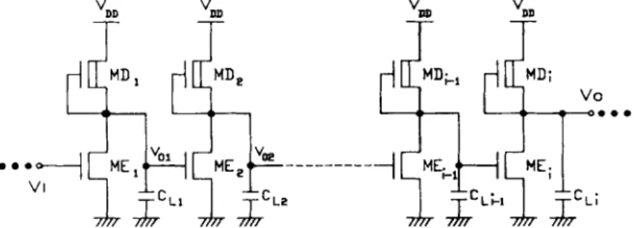
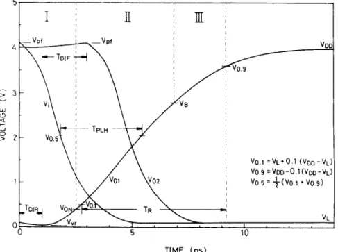
Consider a string of identical E / D NMOS inverters as shown in Figure 1 . I f the input of the inverter string is excited by either a fast or a slow input, the output wave-forms after three or four stages gradually converge to the same shape, which is independent of the input excitation wave-forms. This repetitive wave- form, called the characteristic wave-form, has been noted in developing NMOS timing models. 7 3 9 Typical SPICE-simulated falling characteristic wave-forms for 1
.O
pm E/D NMOS inverters are shown in Figure2 . It is seen that when the input voltage Vi rises from its undershooting valley voltage V,, towards the supply voltage VDD, the output voltage V,I first overshoots t o a peak voltage V,r and then decreases
towards the voltage VL of logic '0'. Also indicated in the wave-forms are the fall time T F , the fall delay
TPHL and the initial fall delay TDII:. This initial delay plays a very important role in determining the pair delay of a logic gate, as will be seen later. Besides the input-output wave-forms of the driving stage, the wave-form of the output voltage V0z in the load stage is also shown in Figure 2. The change of V,,Z leads
vDP T vm T vm T VDD o + VI ___--
Figure I . A chain 0 1 identical E / D NMOS inverters
TIME (ns)
450 C.-Y. WU A N D Y.-T. LIN
to different device capacitances of MEZ, and thus to different loading capacitances of the driver stage, and must be considered.
According to the operating regions of the M O S devices in the driving stage, the falling wave-form of
V,I from t = 0 to t = t 0 . 1 (i.e. V,I = V0.1) is divided into four regions as shown in Figure 2 . In region I ,
where Vi rises from Vvr to VONI,” the enhancement NMOS M E I of the driving inverter is operated in the subthreshold region because its gate-source voltage ( = Vi) is smaller than its turn-on voltage VoNI. The depletion NMOS M D I is operated in the inverse linear region with its upper
n+
region connected to V D D and the lower n+ region connected to Val, which is higher than VDD in region I because of overshooting. Thus, the source/drain nodes o f M D I are interchanged and it is operated in the linear region with a small Vns. In the load stage, the MOS MEZ is in the linear region since V,I ( = VGSZ) is much higher than V,Z ( = VDSZ).In region 11, the final boundary is set to the point where V,I falls back to VDD after overshooting. In this region, the operating region of the NMOS M E I is changed from the subthreshold region into the saturation region, while those of M D I and M E Z remain unchanged. Regions I and 11 are two specific regions with abnormal device operation and distinct transient behaviour. The pair delay, however, is dominated by these two regions and the corresponding regions in the rise time case. Thus they have to be carefully characterized. Regions I11 and IV also have their own device operation regions which, together with those of regions 1 and 11, are given in Table I. The boundary between regions I I I and IV is at V0l = V B , where
V B is the saturation drainlsource voltage of the depletion NMOS M D I under the substrate bias. I t can be calculated by using the suitable model equations in SPICE.
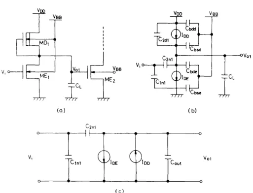
Generally, the large-signal equivalent circuit of a n E/D NMOS inverter can be drawn as shown in Figure
3, where the device capacitances Clnl (unused), Cznl and C,,, as well as the device currents IDD and IDE
have different expressions in each of the four regions. The output capacitance C,,, has three different
parts, namely the device capacitances of
ME^
and M D I , the fixed external load capacitance CL and the equivalent input capacitance of the load stage. Through the equivalent input capacitance in the load stage, the large-signal equivalent circuit for the fall time calculations can be decoupled and reduced to that ofa n inverter with a suitable C,,(.
The wave-form of the input voltage Vi can be approximated by an exponential function with a single effective pole
Pi,
asK ( t ) = D i r exp(- Plrt)+DZr (1)
where P I , , D I , and Dzr are determined to match the wave-form at Vi = Vvr, V0.1 and VB within the first
three regions in Figure 2 .
Region I . Based on equation (I), the time interval tl of region I , i.e. from Vi = Vvr to Vi = VONI, can be expressed as
1 VONI - D z ~
t l =
-
- In(D 1 r
)
PI rTable I. Operating regions of the associated MOSFETs in E/D NMOS inverters
Regions I I I I l l IV
Linear Saturation cut-off
-
-
Rise time case M E I
Mui Saturation Saturation Linear
ME^ Subthreshold Saturation Saturation to linear
-
Saturation?
Subthreshold Saturation Saturation
Fall time case M E I
Mui Inverse linear Inverse linear Linear Saturation
Linear Linear Saturation
M E Z Linear
SIGNAL TIMING OF E/D NMOS L O G I C 45 1 I I
77LA
V,-
C 2 n l ( C )Figure 3 . Large-signal equivalent circuit of a n E/D NMOS inverter
According to the large-signal equivalent circuit of Figure 3, we have
During [ I , the change of VOt is much slower than that of Vi, so the term dV,I/df can be neglected as
compared with dV,/dr. The drain current I D L at f = 1 1 is calculated by using the subthreshold current equations listed in Table 11. The drain current fl)l) of the depletion NMOS M D ~ at t = t l can be calculated by using the linear region current equations in Table 11. Since VGS = VDS = VOI ( t i )
-
VDu in M D l and their values are very small,ZDD
can be simplified aswhere
From the above considerations a n d using equations (4) and ( I ) , equation (3) can be used to solve V,I (fI),
which is
( 5 )
1
B2
vo
I ( t I ) = - [ c21, I p I r (D2 I - V O N 1 ) - I D E ( f I ) - c 21
where Czn1 = CgdoveI W e , . It should be noted that when Vi = VONI at t = t i , V,I has not yet reached the peak point, i.e. V,I(/I) f Vpr.
452 C:Y. W U A N D Y.-T. L I N
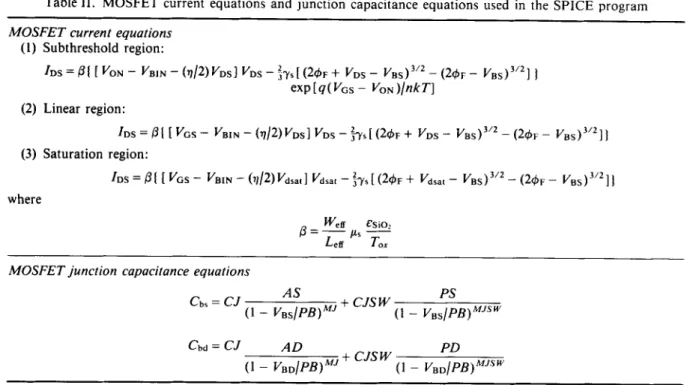
Table 11. MOSFET current equations and junction capacitance equations used in the SPICE program
MOSFET current equations
( 1 ) Subthreshold region: I D S = P ( [ Y O N - V B l N - ( t ) / 2 ) V D S I V D S - $ y s [ ( 2 & F + V D S - V B S ) 3 / 2 - ( 2 f $ F - V B S ) 3 / 2 ] 1 exp[q(VGS - V o ~ ) / n k T l (2) Linear region: I D S = P ( [ V G S - V B I N - ( q / 2 ) V D S l V D S - ~ S [ ( ~ & F + V D S - V B S ) 3 ’ Z - ( 2 & F - V B S ) 3 ’ z I ] (3) Saturation region:
I D S = [ VGS - VBIN - (?1/2) Vdsac
1
Vdrat -frs
[ ( 2 & F+
Vdsat - V B S ) 3/2 - (&F - VBS)3’2] 1 where~
MOSFET junction capacitance equations
Note: The parameters in this table are from SPICE level-2 device models.”
Region 11. In region 11, the device capacitances Cznl and C,,, can be expressed by using Meyer’s model,
’‘
which is also used in SPICE. The expressions are given in Table 111. In equation (2a) of Table 111, the value 1+
I
A u ] is the factor used in Miller’s theorem to calculate the equivalent input capacitance due to Cznz of the load stage. In the load stage, although the MOS MEZ is operated in the linear region, its output voltage is nearly unchanged during the whole interval of region I1 and can be treated as shorted to ground in the large-signal analysis. This means Au = 0 in the capacitance calculation. The voltage-dependent sourceldrain junction capacitances in the above expressions are linearized by a fixed value calculated at a constant junction bias. This bias is chosen to be that at the central point of each region. The linearized junction capacitances C h d e l and Chddl in region I1 can be calculated from the SPICE equation with thereverse junction bias fixed at VDD for linearization. Now, CZ”I and C,,, become linear capacitances. The MOS M E I is operated in saturation and its drain current equation in SPICE is given in Table 11. This equation is too complicated to be used in obtaining the analytic solution for V , I ( ~ ) from equation (3). Here we use a least-square curve-fitting method to model the current with a simplified formula which has a good accuracy and can be treated analytically in equation (3). In this method, the ranges of VL\ and VDS for current calculations are determined first. I n region 11, the initial boundary is V , = V O N ~ and V,I = V o I ( f l ) and the final boundary is V0l = VDD. The value of V , at the first boundary of region I1 is greater than V O N ~ and is unknown. For the purpose of current calculations, we assume that the value of
V , at the final boundary is 2 V 0 ~ 1 , which is a good approximation. Then the above range is equally divided and four sets of V, and V,I (i.e. VGS and VDS) can be obtained. Using the four sets of voltages in the saturation current formulae to calculate the drain current and then using the least-square fitting method, we have
( 6 )
where the constants Als, AzS and ClS are determined from the least-square fitting method with a typical error of 7 % . In equation ( 6 ) , the term AzSV?(t) is mainly contributed by the term VGSVdsate in the expression of the saturation current; since Vdsate is dependent upon V G S = V,, it is V&s-dependent or
V:-dependent. Another current, I D D ( f ) , has been characterized in equation (4) with t~ replaced by t . / D E ( f ) = A z s V : ( f )
+
A l s V , ( f )+
CISSIGNAL TIMING OF E / D NMOS LOGIC 45 3 Table 111. The corresponding output capacitance of a n E/D NMOS inverter in the individual regions of rising/falling
tme period
A u = - 1
The V,I in the s-domain can be solved from the equivalent circuit. The detailed procedure is given in Appendix 11. Taking the inverse Laplace transformation of V O l ( s ) , V o l ( t ) in region I1 is solved as
Vot(t)=
Fte-2P"'+ F2ecP'i'+ F 3 e C P t ' + F 4 (7)Letting dVol(t2)/dt=0, the time t2 when V,I reaches the overshooting peak Vpf can be obtained.
Therefore the initial fall delay TDIF can be expressed as T D ~ F = tl
+
r2.
Additionally, the input voltage used as the initial value Vf!' of region 111 is calculated at V0l = VDD.454 C.-Y. WU AND Y.-T. LIN
Region 111. In region 111, the MOS MDI returns t o normal operation with its gate and source shorted
together and provides a current to charge the output capacitive load. However, the pull-down current I D E has exceeded the pull-up current ZDD and their difference becomes more and more prominent, leading to an output voltage falling down faster than rising up. This is because the driving capability of the MOS
M E I is larger than that of M D I owing to the larger beta ratio which is necessary to retain a reasonable noise
margin. As seen in Figure 2, the MOS M E I is operated in the saturation region whereas the MOS M D I
is operated in the linear region during the time interval of region 111. The value of
1
AuI
is empirically fixed to be zero according to the changes of V0l and V02 in region 111.The large-signal equivalent circuit is similar to Figure 3 and the Kirchhoff‘s Current Laws (KCL) equation is the same as equation (16) of Appendix I1 except that IDD is expressed as
B21 Vol ( 1 )
+
C21 (linear region)B Z ~ V ~ I ( t )
+
CzS (saturation region)IDD(1) =
The least-square current-fitting method is also applied to model the depletion MOS current with Vcs = 0. The currents in both saturation and linear regions can be linearized by straight lines whose equations are given by (8).
With four different sets of voltages within the range from V, = V!!’ to Vi = VB + ~ V O N ~ , another current, I D € , is expressed by using the curve-fitting method in the same way as for equation (6) in region
11. Although the final boundary of V , may deviate slightly from the chosen value, equation ( 6 ) can still
accurately characterize the drain current of ME^. In other words, the approximation of the device current is less sensitive to the final boundary condition. The induced error is then tolerable.
Except that the gate-drain capacitance Czn1 can still be expressed by equation (1) of Table 111, the contribution of device capacitances to CoUI is different from that in region 11, mainly caused by the MOS
M D I now with its gate shorted to its source. CoUI is expressed as listed in Table 111. Note that the value of VDS at the central point of region I1 is taken to linearize C g d d l , C b d c l and CWI. In addition, A u is set to zero as discussed before. It should be noted that Meyer’s capacitance model in SPICE has been adopted to express the gate-drain capacitance C g d d l , which changes continuously from the highly linear region to the slightly linear region of M D I . On the other hand, the capacitances Cgdez and CgScz are assumed to be ;Coez, a good approximation for the MOS MEZ in the highly linear region with a large V G S . After capacitance linearization, all capacitances become linear. The output V0l ( 1 ) in region 111 is then expressed as equation (7) with
Pf
= - B~I/CT. The time TFI from V0.9 to Vtl is then calculated from VoI ( 1 ) .Region IV. In region IV, the operation of inverters with short-channel devices ( L m a r k = 1.0 pm) is different from that of inverters with long-channel devices ( L m a r k = 3.5 pm). From SPICE transient data, we find that even though V, is raised to a high Level in region IV, the saturation voltage VdSarel for short- channel devices is still very small. Thus in region IV, the MOS M E , is mostly operated in saturation. However, for long-channel devices, the MOS M E I changes its operation region from the saturation region to the linear region instead. From SPICE DC analysis, the saturation voltage Vdsate of 1.0pm enhancement NMOS at VGS = VDD is about 0 - 6 7 V, implying that the MOS M E ( is always operated in saturation even when the output voltage has fallen to Vo.1. But for 3.5 pm enhancement NMOS, the saturation voltage Vdsate is about 2.3 V when VGS = VDD. Thus the MOS M E I changes its operation region to the linear region when the output voltage falls below 2.3 V. In developing this timing model, both the above cases were considered, but only the short-channel case is discussed in the following analysis.
According to the output response derived in region 111, the value of Vi at V,I = VB can be obtained, which is the initial boundary of region IV. Because of the same operation region of the MOS M E I in both regions I11 and IV, equation ( 6 ) is still used to approximate the pull-down current ZDE. The pull-up current
IL)D has the same form as equation (8b).
I n region IV, the expression of Co,,I is similar to equation (3a) of Table I11 except that MDI is operated in the saturation region and the voltage gain Au should be considered. The gate-drain capacitance C g d d l is now equal to zero. The voltage gain Au is empirically determined to be -0.5. In addition, because the
SIGNAL TIMING OF E/D NMOS LOGIC 45 5 MOS MEZ is in saturation, we have
Cgde-2 = 0 Cgse-2 =
:
C O C ZFor the input voltage Vi, the expression of equation (1) is used but with Dlr, D2r and PI, replaced by El,,
Ez,
and P2,. These three new constants can be obtained from the calculation of the rise wave-form in region11. The resulting formula is the same as equation ( 7 ) but with Pf =
-
BzJCT. From the formula, the timeinterval TFZ from VB to Vo.1 can be determined.
Combining both output responses in regions 111 and IV, we obtain the fall time TF as
TF = T F I
+
TFZ (10)Note that TF is a function of the rise poles PI, and Pz,. 2.3. Rise time
In the rise time case, the simulated characteristic wave-forms are shown in Figure 4 with three divided regions. The operation regions of the associated MOS devices in each region are listed in Table I. Note that the MOS M E I in the driver stage is turned off for most of regions I1 and 111. Thus the input waveform has only a limited effect on the rising output, as already recognized in Reference 10.
Region I . The purpose of defining region I is to calculate the initial rise delay. From Figure 4, it is seen
that when V, falls quickly from Vpf to VL, the output voltage of the driver stage initially at V L first undershoots to a valley voltage V,, and then rises slowly towards VDD. This undershoot is related to the inital rise delay T D I R . Because all the device currents in this region are extremely small, the input wave- form near the peak point is fairly importnat for the initial delay calculation and has to be accurately modelled. Thus the wave-forms in regions I1 and I11 of the falling wave-form are taken into account and approximated by the following single-pole response:
Vi(f) = ( Vpf - Vdexp( - P i d )
+
VITIME (ns)
456 C.-Y. WU AND Y.-T. LIN
To find the effective pole P l f , we choose the point at t = [B when
Vi
= VB as the matching point. Thus Plf can be solved aswhere VB and t B have been modelled in the fall time case. It is found that this approximation can dramatically improve the accuracy of the initial delay calculation.
In region I, the depletion current of MDI is still the same as equation (8) in the saturation region. Because the MOS
ME^
in the load stage is cut off, its output voltage is nearly unchanged so that the miller effect can be neglected (i.e. Au = 0). On the other hand, the MOS M E I is in the linear region and its drain current as shown in Table I1 includes the ViVol(vGSVDS) term. This term has to be linearized to obtain the analytical expression for the output voltage. It is found that simple linearization of A 1 1 V,+
Bl1Vol is unable to linearize the6
V,I term with a good accuracy. Instead, the following expression to decouple theK V O l term is proposed and has proved to be satisfactory:
(12) where the coefficients A I I , A ~ I , BII and CII are calculated by using the least-square fitting method with four sets of (Vi, Val) equally divided in region I. In equation (12), the V? dependence is caused by the strong dependence of the output wave-form V,I upon the input V, during the voltage undershoot.
The large-signal equivalent circuit in the rise time case is the same as shown in Figure 3 but with different device capacitances according to the different device operation regions. The general form of the total output capacitance is given in Table 111. For accurate calculations, the weak inversion of the MOS
ME^
should be taken into consideration. Its gate-source and gate-bulk capacitances2' are also listed in Table 111. In equations (5b) and (5c) of Table 111, VGSZ represents the midpoint of the output wave-form in region I, which is used for linearization. Substituting equation (4) of Table 111, equations (8) and (12) into equation (16) of Appendix 11, we obtain an expression of the output voltage wave-form similar to that in equation (7). The initial rise delay TDIR can be obtained by taking dVoI (TDIR)/dt = 0. Thus the pair delay is expressed as
TPD = TDIF
+
TDIR I D E ( s ) = A z ~ ?+
A ~ I K+
B l l ~ o l+
c I ~ / s(13) Additionally, the input voltage at V,I = VON2 is found, which serves as the initial value of region I1
Region II. The MOS ME' in region I1 is not always off. For inverters with a particular beta ratio, it may be operated in saturation. Thus the MOS ME' is assumed to be in saturation and its current equation is approximated by equation (6). If the device is off, the resulting equation (6) will be very small. Thus the above two cases can be characterized as well. From Table I, the MOS M D I is in saturation. Its current expression is given in equation (8).
In the calculations of regions I1 and 111, the fall pole in equation ( l l a ) is replaced by Pzf, which is determined as
(14) 1
P 2 f = - ln(9) TF
As seen in Figure 3, the capacitance Cznl is the same as that in region I. The output capacitive load Gout
can be expressed as equation (4a) of Table I11 without the terms Cgbe2, C g d d l and Cgde2. The term Au is set to .- 1 . Since the MOS MEZ is operated in the saturation region, the gate-source capacitance CgSez is
estimated to be
5
Coe2. Then the output expression can be solved similarly to that in equation (7). The time interval from V0l = Vo.1 to Vol = V B , which is called T R I , can then be obtained.Region III. The analysis of region I11 is much simpler than that of any other region. The MOS M E '
SIGNAL TIMING OF E/D NMOS LOGIC 457
Its current is expressed in equation (8). As may be seen from SPICE transient data, it is found that the MOS MEZ in the load stage is operated in saturation first and then in the linear region. To simplify the analysis, the capacitances in the two regions are averaged. The resulting expressions are listed in Table 111. The calculated output response is solved similarly to that in equation (7). Thus the time interval T R Z
between VOl = VB and VoI = v 0 . 9 can be calculated. Finally, the rise time TR is obtained as
TR = T R I -k TRZ (15)
Note that TR is a function of the fall poles P l f and P N . Numerical iterations are thus required to solve T R and TF. The iteration method is described below.
2 . 4 . Calculation method
Since the rising output wave-form is nearly indpendent of the input wave-form, we can roughly calculate the rise time T R and the rise poles P I , and Pz, by assuming that the MOS M E , is off and only the MOS M D I charges the output capacitive load with a step input excitation, i.e. Plr, P2r -+ 00. The solved rise poles are then used as the initial guess in the fall time calculations. After the fall time TF has been obtained from the calculation, it is transformed into the fall poles Plf and P2f in equations ( l l b ) and (14) respectively.
These are then used in the rise time calculation to obtain a new
TK.
The iterations are stopped when the error between two successive iterations has been reduced to a specified value. Then all the timing data(TR, T F , T D I R , T D I F , T P D , T P L H , T P H L , etc.) can be obtained. Generally, the number
of
iterations is less than three with a final error of 5% between two successive iterations. Thus the computer time consumed is quite small.3. COMPARISONS WITH SPICE SIMULATION RESULTS
To verify the accuracy of the modelling method, we used the same device current and capacitance equations as in SPICE, and SPICE simulations were performed for comparisons. Wide-range comparisons are given to verify the generality of the models in characterizing inverters with different beta ratios, sizes, device parameters, input wave-forms and capacitive loads. Some of the comparisons will be presented in
this section.
There are three kinds of error sources in this timing model. The first is due to the linearization on various voltage-dependent MOSFET channel capacitances and p - n junction capacitances. The second arises from
the single-pole assumption for the input wave-forms used in the calculations of output responses. The last is due to the drain current approximation. The effects of these error sources will be investigated later.
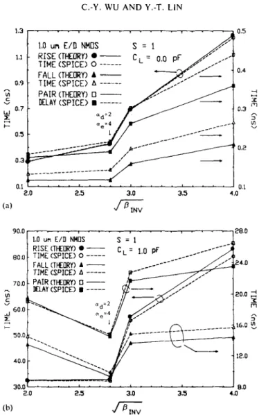
I n Figure 5 we show the rise time, fall time and delay time of characteristic wave-forms in 1.0 pm E/D NMOS inverters with different capacitive loads. Similar data for 3.5 pm E/D NMOS inverters are listed
in Table I V for different size factors S . It is seen from these comparisons that for large fixed capacitive
loads CL (CL 2 0.1 pF for 1 a 0 pm and CL
2
0 - 5 pF for 3.5 pm) and S = 1, the calculation errors of rise time and pair delay are below 12%, while those of fall time are below 8%. This is because all the internal device capacitances become negligible compared with the load capacitance CL. Thus the error in this caseis from the drain current and input wave-form approximations. It is also shown that for small-size inverters with S = 1 and large C L , the errors remain nearly the same for different CL values. However, for S = 10 the internal device capacitances contribute another error source and the errors deviate when CL changes.
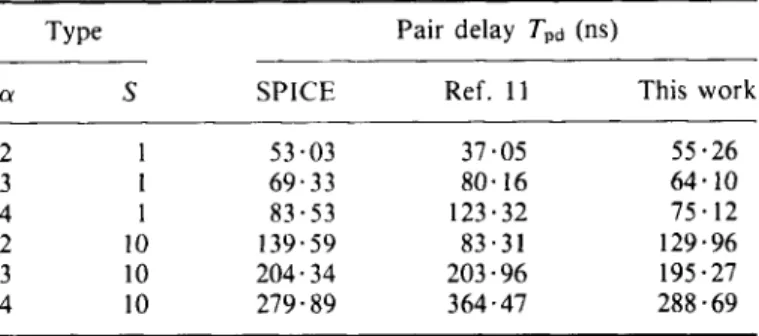
Listed in Table V are the calculation results of this work and the model developed by Auvergne et a / .
for 3.5 pm inverters. I t is found that the errors are comparable in the two models for (Y = 3, but for small
and large values of CY the error of Reference 11 is worse. The possible cause is the assumption of a ramp input, the oversimplifying expressions of device currents and the rough definition of device operations as discussed in Reference 11.
458 C.-Y. WU A N D Y.-T. LIN Figure 5 . Comparisons (b) CL = 1 of .O 1.0 un E/D NMOS TIME (SPICE) 0 --- FALL (THEORY) A
-
PAIR (THEORY) 0-
DELAY (SPICE) B ---__---
-
_____--- 2.0 2.5 3.0 3.5 4.0 (a)G
1.0 UPI E/D NMOS S = l
RISE (THORY) 0
-
c = 1.0 p~TIME (SPICE) 0 ---
--A
24.0 ___---- FALL (THEORY) A-
TIME (SPICE) A --- P'-----
3O.OT ' . . . ' . ' . . ' . . ' . ' - ' J 8.0 2.0 2.9 3.0 3.5 4.0 (b)m
T
v
calculated SPICE simulated rise/fall/delay times of 1 .O pm E/D NMOS inverters: (a) pF. All inverters are designed with a d = ae = , B , N ~ except the one indicated in the figure
CL = 0 pF;
Table IV. Errors of rise/fall/delay times in the case of characteristic wave-forms for 3.5 p n E / D NMOS inverters with different sizes and different capacitive loads
S 1.0 10.0 f f d 2.0 4.0 1.0 16.0 2.0 4.0 Dimension ffe 2.0 4 .0 16.0 1.0 2.0 4.0 Error (To) 0 p F T R 1.65 5.27 -4.92 20.78 10.57 14.87 TF 2.03 -8.35 - 14.76 1.08 - 4.09 0.73 TP D - 1.65 2.16 - 17.46 - 7.91 - 13.77 1.48 0.5 p F T R 2.79 7.69 0.35 11.21 9.74 15.10 TF 4.63 -4.23 - 7.69 -2.96 0-20 0.57 TPD 3.90 - 1.62 - 10.79 - 5.05 - 10.87 - 1.44 2 - 0 p F T R 3.10 8.21 1.14 10-13 9.15 12.87 TF 4.71 - 3.63 -5.42 -3.10 4.94 2.02 T P D 4-20 - 9.96 - 8.22 - 11 -66 - 6.90 3.15
SIGNAL TIMING OF E/D NMOS LOGIC 459 Table V. Comparisons of SPICE simulated pair delay times with
those calculated by the models in Reference 11 and this work
~~ ~
Type Pair delay Tpd (ns)
a S SPICE Ref. 1 1 This work
2 1 53.03 37.05 55.26 3 1 69.33 80.16 64.10 4 1 83.53 123.32 75.12 2 10 1 3 9 3 9 83.31 129.96 3 10 204.34 203.96 195.27 4 10 279.89 364.47 288.69
has to be retained under these variations. To test the capability of the developed timing model in this respect, extensive comparisons between SPICE simulation and model calculation results were made for inverters with different values of the device parameters. Some of the comparisons are listed in Table VI for a 3.5 pm E/D NMOS inverter with a beta ratio of 9. In this table, the variations in VTO, To,, Uo and
V
M
(SPICE” parameters) as well as two different variation cases, called the fast case and the worst case,~
~
are considered. The resulting error is similar to that in the normal case. Thus the developed model is still applicable under these inevitable process variations. This generality comes from the fact that all the SPICE device parameters are considered in the timing model.In the developed timing models, although the equations are derived from consideration of the characteristic wave-form, the effect of input wave-forms is considered through the use of the least-square curve-fitting method. The timing models can therefore handle the non-characteristic wave-form cases mentioned above. To show the capability of this timing model to deal with step input excitations, examples are given in Table VII for inverters with different beta ratios and capacitive loads. In this table, we calculate the propagation rise/fall delay instead of the initial rise/fall delay, because it is the delay of the stage connected to the external input. As shown in Table V I I , the maximum error is less than 33% for riselfall times and less than 29% for propagation rise/fall delays.
The simulated and calculated signal timings for the exponential input as a function of the normalized
Table VI. Errors introduced from variations of threshold voltage; gate oxide thickness, mobility and maximal drift velocity for an E / D NMOS inverter with different load capacitance, including fast-speed case and worst-performance
case
A V T O ( ~ ) A To.r(A) AUo (m2/V - s ) A V M ~ X ( m s - ’ )
Error Fast Worst
(VO) -0.16 +0.16 -60
+
60 - 5 0 + 5 0 - 2 lo4 ~ + 2 x lo4 case caseO p F TR 4.83 4.57 4.44 5.04 4.81 4.69 5.42 5 - 0 8 4.69 5.01 TF - 4 . 7 1 -2.81 - 4 . 3 0 -3.01 -3.26 -3.60 -3.82 -3.63 -5.49 - 1 . 8 5 T P D -8.04 2.51 -11.59 -12.00 -11.88 -11.47 -11.14 -11.89 -8.19 3.76 0 . 5 p F TR 6.78 7.28 7.50 7.48 7.34 7.39 6.78 7.54 7.15 7.33 TF -1.10 0.31 - 0 . 8 0 0.06 0.04 -1.29 -1.40 -0.97 -1.19 0.96 T P D -8.70 -0.41 -7.95 - 7 . 5 0 -8.06 -7.39 - 6 3 4 -7.81 9.83 0.44 2 . 0 p F TR 7.49 7.87 7.29 7.74 7.90 7.64 7.09 8.17 7.69 6.80 TF - 0 . 5 8 1.44 -0.37 1.06 1 . 1 1 0.54 0.67 0.17 -0.80 0.25 T P D 9.93 -2.90 -7.75 -7.35 -7.43 -7.33 - 5 - 9 3 -7.73 10.81 -2.23
460 C.-Y. WU AND Y.-T. LIN
Table VII. Errors of rise/fall/delay times of E/D NMOS inverters with different load capacitances and driven by a step input (Y 2 4 CL (PF) 0 0.5 1.0 2.0 0 0.5 1.0 2.0 TR (ns) SPICE 2-32 23.63 44-91 87.53 8.10 54.91 101.80 195.40 Theory 2.11 23.23 44.19 86.46 7.87 57.47 107.05 206-70 Error(%) -9.15 -1.68 -1.61 -1.23 -2.80 4.67 5 . 1 5 5.78 TF fns) SPICE 0.746 7-43 14.16 27.63 0.44 2.79 5.32 9-78 Theory 0.501 5.19 9.86 19.19 0.41 2.77 5.12 9.80 Error(%) -32.82 -30.15 -30.37 -30.56 -6-87 -0.79 -3.88 0.17 TPLH (ns) SPICE 0.920 9.46 17.93 34.86 4.68 25.78 47.40 90.62 Theory 1.136 11.72 22.27 43.29 4.53 30.24 56.08 107.57 Error(%) 14.48 23.86 24.19 24.17 -4.81 17-32 18.30 18.70 ~~~ TPHL (ns) SPICE 0.270 2.67 5.04 9.82 0.200 1.27 2.32 4.55 Theory 0.194 1.92 3.64 7.08 0.157 1.01 1.86 3.55 Error(%) -28.20 -28.25 -27.82 -27.90 -21.41 -20.78 - 19.99 -21.90 CY = L d / W d = We/Le; Le = Wd = 3 . 5 pm.
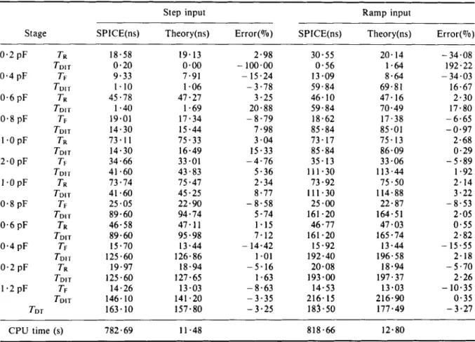
Table VIII. Timing data obtained from this work and SPICE for a chain of 12-stage E/D NMOS inverters with different capacitive loads and driven both by a step input and a ramp input ( T F = 80 ns)
~ ~ _ _ _ _
Step input Ramp input
Stage SPICE(ns) Theory(ns) Error(%) SPICE(ns) Theory(ns) Error(%)
0 .2 pF TR TVIT 0.4 pF TF TVIT 0 .6 pF TR 0.8 pF TF l * O p F TR TDIT TDIT TVIT 2.0 pF TF TDIT T D i T TVIT TDIT TDIT TVIT TVIT I . O pF TR 0.8 pF TF 0. 6 pF TR 0.4 pF TF 0 .2 pF TR 1 . 2 p F TF TDT CPU time (s) 18-58 0.20 9.33 1.10 45.78 1.40 19-01 14.30 73.11 14-30 34.66 41 -60 73-74 41 *60 25.05 89.60 46-58 89-60 15.70 125.60 19.97 125.60 14.26 146.10 163-10 782 * 69 19.13 0.00 7.91 1.06 47.27 1-69 17.34 15-44 75.33 16-49 33.01 43.83 75.47 45.25 22.90 94.74 47.11 95.98 13.44 126.86 18.94 127.65 13-03 141.20 157.80 2.98 - 100.00 - 15.24 - 3.78 3-25 20.88 7.98 3.04 15.33 5.36 2.34 8.77 - 8 . 5 8 5-74 1 . 1 5 7.12 - 14.42 1-01 -5.16 1 a63 - 8.63 -3.35 - 3.25 - 8.79 -4.76 30-55 0.56 13.09 59.84 46.10 59.84 18.62 85-84 73.17 85.84 35.13 111.30 73.92 111.30 25.00 161 -20 46.77 161 -20 15.92 192.40 20.08 193.00 14-53 216.15 183.50 20.14 1-64 8.64 69.81 47.16 70.49 17.38 85.01 75.13 86.09 33.06 113.44 75-50 114.88 22 * 87 164.51 47.03 165.74 13-44 196.58 18.94 197.37 13.03 216.90 177.49 - 34.08 192.22 16.67 2.30 17.80 - 6.65 - 0.97 - 34.03 2.68 0.29 1.92 2.14 3.22 2.05 0.55 2-82 - 15.55 2-18 - 5.70 2.26 0.35 -5.89 - 8.53 - 10.35 -3.27 11 a48 818.66 12.80
SIGNAL TIMING OF E / D NMOS LOGIC 80- 6 0 -
-
46 1 RISE (THEORY)-
TIME (SPICE) o ---- FALL (THEORY) A-
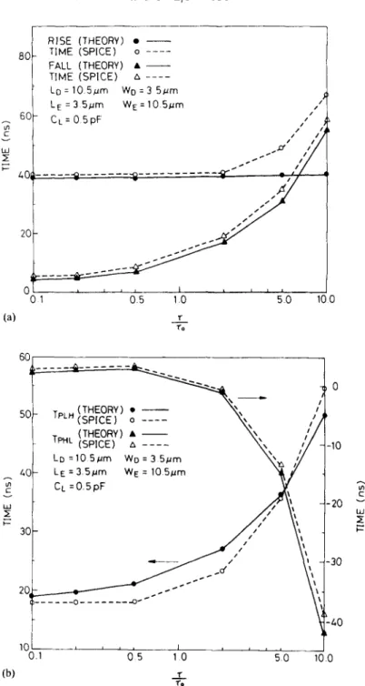
TIME (SPICE) A - - - - Lo = 10 5 p r n WI, = 3 5 p r n I L E = 3 5 p m WE = 10 5wm I I C ~ = 0 5 p F I , j I 10 0 5 1 0 5 0 100 0.1 r r.-
(b)Figure 6. Rise/fall/delay times of 3.5 pm E/D NMOS inverters with exponential inputs
transition ime 7/70 are shown in Figure 6. Similar error characteristics are also found in the ramp input case. The normalized transition time, which ranges from 0.1 t o 10, incudes both the fast input and the slow input excitations. The calculation method is similar except that the input wave-form function is
known. In the case of exponential inputs in Figure 6, less than 17% error is obtained for 7/70
<
1. However, when 7/70>
1, the error in the rise times increases t o-
39% because of the inadequate device operation assumed in region 111 of the rise time. The magnitude of the propagation fall delay in the case462 C.-Y. WU AND Y.-T. LIN
contribution of this term to the pair delay is negligible and can be ignored. From the above comparisons, it is shown that the proposed timing models can be applied to any input wave-forms up to 10 times as fast or slow as the characteristic wave-form.
4. APPLICATION EXAMPLE
As an application example of the developed timing models in timing analysis, the signal timing of a chain
of 12-inverter stages with different capacitive loads is calculated. The signal timings under both step input and slow ramp input ( T F = 80 ns) excitations are shown in Table VIII. It is seen that the rise/fall times in these two cases have an error of less than 16% except for the first two stages in the ramp input case. In the case of step input excitations, the total initial delay TDIT introduces an error of - 100% in the first stage; this then gradually converges to below 9% after the sixth stage and finally the error of the total propagation delay reduces to less than 4% at the output. Similar error characteristics are found in the case of ramp input excitations.
The consumed CPU time on a personal computer is also listed at the end of Table VIII. Obviously, timing analysis or simulation using the timing models is about 65 times faster than that using SPICE. Moreover, the required memory is also quite small compared with that for SPICE.
5 . CONCLUSION AND DISCUSSION
Based upon the large-signal equivalent circuit and s-domain analysis, a general method is proposed to model the signal timing of E/D NMOS logic analytically. Since the E/D NMOS logic has a wide range of device sizes and beta ratios, the device currents are characterized by the least-square curve-fitting technique. This increases the accuracy of the device current calculations and leads to an analytical timing model. In addition, the initial delay, which has a wide range of values even for inverters, is modelled in detail by considering the small device current.
By applying the proposed modelling method to E/D NMOS inverters, their rise time, fall time and delay time have been successfully expressed by analytical equations. Extensive comparisons with SPICE simulation results have shown that the derived general models have a good accuracy for inverters with different device dimensions, inverter sizes, capacitive loads, beta ratios, device parameters and input excitation wave-forms. The required CPU time and memory for the calculation are quite small. Two examples are given to demonstrate the applications of the derived methods in timing analysis of E/D NMOS inverters.
Although the proposed modelling method is only applied to the case of E/D NMOS inverters in this paper, it can be applied to other E/D NMOS gates such as NAND, NOR, etc. Since the timing models derived from the proposed method are analytical, their applications to automatic sizing and optimization of E/D NMOS logic gates are highly expected.
APPENDIX I: NOTATION
voltage gain
bulk-drain p-n junction capacitance of an enhancement (depletion) n-channel MOSFET in the ith inverter stage
bulk-source p-n junction capacitance of an enhancement (depletion) n-channel MOSFET in the ith inverter stage
gate-bulk overlap capacitance of an enhancement (depletion) n-channel MOSFET in the ith inverter stage
gate-drain overlap capacitance of an enhancement (depletion) n-channel MOSFET in the ith inverter stage
gate-source overlap capacitance of an enhancement (depletion) n-channel MOSFET in the ith inverter stage
SlGNAL TlMlNCi OF E/D NMOS LOGIC 46 3 fixed load capacitance of an inverter stage
channel oxide capacitance of an enhancement (depletion) n-channel MOSFET in the ith inverter stage
mask channel length of an enhancement (depletion) n-channel MOSFET in the ith inverter stage effective channel length of an enhancement (depletion) n-channel MOSFET in the ith inverter stage
mask channel length of the MOSFET size factor of an E/D NMOS inverter
the time when V0l = V B in the fall time calculation
time interval from undershooting valley (overshooting peak) of the rising (falling) input to
overshooting peak (undershooting valley) of the falling (rising) output total initial delays from the first stage to a referred stage in Table VIII
total propagation delay between the point the input voltage changes to V0.s and the point the output voltage of the last stage changes to v0.5 in Table VIII
time interval from the rising (falling) input voltage at v 0 . 5 to the falling (rising) output voltage
at v0.5
fall (rise) time defined as the interval of a falling signal from V0.9( VO. I ) to V0, I ( V0.9)
the time when the output voltage is equal to V0.l
the output boundary of the saturation and linear regions for the gate-source-shorted depletion n-channel MOSFET in an inverter
power supply voltage
saturation voltage of an enhancement (depletion) n-channel MOSFET voltage level of the logic state ‘0’
initial voltage in region x of the falling characteristic wave-form
turn-on voltage of an enhancement n-channel MOSFET in the ith inverter stage
voltage at overshooting peak (undershooting valley) of the falling (rising) characteristic wave-form
the voltage VL
+
0 - 1 ( VDD - VL) the voltage VDD - 0 - 1( V D D - VL)the voltage :(VO.I
+
v0.9)mask channel width of an enhancement (depletion) n-channel MOSFET in the ith inverter stage effective channel width of an enhancement (depletion) n-channel MOSFET in the ith inverter stage
beta ratio of the E/D NMOS inverter,
PINV
= (We/Le)/( Wd/Ld)square root of the beta ratio, i.e. a = $INV
the ratio Ld/Wd of a depletion n-channel MOSFET the ratio We/Le o f an enhancement n-channel MOSFET
Fermi potential o f the enhancement (depletion) n-channel MOSFET in the ith inverter stage transition time of an input signal
transition time of the characteristic wave-form
effective surface mobility of the enhancement (depletion) n-channel MOSFET in the ith inverter stage
7
APPENDIX I1
As seen in Figure 3, substituting equations ( l ) , (4) and ( 6 ) in equation (3) and taking the Laplace
transformation with the initial values of Vi and V0l as VONI and V O l ( t l ) respectively, we have
(16) It should be emphasized here that in finding f D E ( s ) , V ? ( t ) is first calculated from equation (1) and then transformed into the s-domain. Thus
Kz(s)
in I V E ( S ) is not Vi(S)Vi(S). The solved and factored V 0 l ( s )464 C.-Y. WU AND Y.-T. LIN from equation (16) is F 3
+ -
F 4 FI F 2 VOI(S) = ~+
-+
- s + 2 P 1 r S + PI, S + Pr s REFERENCES1. E. Seewann, ‘Switching speed of MOS inverters’, IEEE J. Solid-Stare Circuits, SC-15, 246-252 (1980). 2. A. Kanuma, ‘CMOS circuit optimization’, Solid-State Electron., 26, 47-58 (1983).
3. M. Horowitz, ‘Timing models for MOS circuits’, Ph.D. Disserlation, Stanford University, 1983.
4. T. Tokuda, K. Okazaki, K . Sakashita, I . Ohkura and T . Enomoto, ‘Delay-time modeling for E D MOS logic LSI’, IEEE Trrons. 5. D. Etiemble, V . Adeline, N. H. Duyet and J . C. Ballegeer, ‘Micro-computer oriented algorithms for delay evaluation of MOS 6. C . Y . Wu and J. S. Hwang, ‘Efficient timing models for characteristic waveforms of CMOS logic gates’, in Proc. 27th Midwessl
7. R. J . Bayruns, R. L . Johnston, D. L. Fraser, Jr. and S.-C. Fang. ‘Delay analysis of Si NMOS Gbit/s logic circuits’, IEEE J.
8. J . A. Pretorius, A. S. Shubat and C . A. T . Salama, ‘Analysis and design optimization of domino CMOS logic mith application 9. C.-Y. Wu, J . 3 . Hwang, C . Chang and C.-C. Chang, ‘An efficient timing model for CMOS combinational logic gates’, IEEE 10. J . G . Simmons and G . W. Taylor, ‘An analytical treatment of the performance of submicrometer FET logic’, lEEE J. Solid-
11. D. Auvergne, G . Cambon, D. Deschacht, M. Robert, G. Sagnes and V. Tempier, ‘Delay-timeevaluation in E D MOS logic LSI’, 12. M. D. Matson and L. A. Classer, ‘Macromodeling and optimization of digital MOS VLSI circuits’, IEEE Trcrns. Cotnputer- 13. N . Hedenstierna and K . 0. Jeppson, ‘CMOS circuit speed and buffer optimization’, IEEE Trans. Co/npir/er-Aided Design, 14. C. Y . Wu and M. C. Chiau, submitted to IEEE Trans. CAD Integ. Circ. Syst.
IS. J . K. Ousterhout, ‘A switch-level timing verifier for digital MOS VLSI’, IEEE Trans. Compuler-Aided Design, CAD-4, 336-349 16. N. P. Jouppi, ‘TV: An nMOS timing analyzer’, in Proc. 3rd Caltech C o n f , 1983, pp. 403-410.
17. L . A. Glasser, ‘The analog behavior of digital integrated circuits’, in Proc. 18th Design Automation Conf., 1981, pp. 603-612. 18. J . Rubinstein, P. Penfield and M. Horowitz, ‘Signal delays in R C tree networks’, IEEE Trans. Computer-Aided Design, CAD-2,
Computer-Aided Design, CAD-2, 129-134 (1983).
gates’, in Proc. 21st Design Automation Conf., 1984, pp. 358-364. Symp. on Circuits and Sysrems, 1984, pp. 574-578.
Solid-State Circuits, SC-19, 755-764 (1984).
to standard cells’, IEEE J . Solid-Stare Circuirs, SC-20, 523-530 (1985). Trans. Computer-Aided Design, CAD-4, 636-650 (1985).
State Circuits, SC-20, 1242-1251 (1985).
IEEE J. Solid-State Circuits, SC-21, 337-343 (1986).
Aided Design, CAD-5, 659-678 (1986). CAD-6, 270-281 (1987).
(1985).
202-21 1 (1983).
19. J . L. Wyatt, Jr. and Q. Yu, ‘Signal delay in RCmeshes, trees and lines’, in Proc. 1984 Int. Conf. Computer-Aided Design IEEE,
1984. PP. 15-17.
20. C . A. Zukowski, ‘Bounding enhancements for VLSI circuit simulation’, Ph.D. Dissertation, MIT, 1985.
21, A. Vladimirescu and S. Liu, ‘The simulation of MOS integrated circuits using SPICEZ’, Electronic Res. Lab. Memo. UCBIERL-