Optical properties associated with strain
relaxations in thick InGaN epitaxial films
Wen-Che Tsai,1,2 Chia-He Hsu,1 Shao-Fu Fu,1 Fang-Wei Lee,1 Chin-Yu Chen,1 Wu-Ching Chou,1 Wei-Kuo Chen,1 and Wen-Hao Chang,1,*
1Department of Electrophysics, National Chiao Tung University, Hsinchu 30010, Taiwan 2Department of Electronic Engineering, Chung Yuan Christian University, Chung Li 32023, Taiwan
*whchang@mail.nctu.edu.tw
Abstract: Structural and optical properties of thick InGaN layers with
strain and composition inhomogeneities are investigated. High resolution x-ray diffractions (XRD) and reciprocal space mapping (RSM) along an asymmetric axis reveal that the In composition inhomogeneity is accompanied by strain relaxations during the growth of thick InGaN layers. According to the structural analysis, the commonly observed double photoluminescence (PL) peaks have been confirmed to be associated with the strain relaxation in thick InGaN films. Temperature-dependent PL measurements further indicate that the relaxed phase in InGaN films exhibits better emission efficiency than the strained phase. Recombination dynamics reveal that the carrier localization effect is more pronounced in the relaxed phase due to the compositional pulling effect. The correlations between emission efficiency and localization effect in thick InGaN films are discussed.
©2014 Optical Society of America
OCIS codes: (130.5990) Semiconductors; (160.4760) Optical properties; (250.5230)
Photoluminescence.
References and links
1. P. Kung and M. Razeghi, “III-Nitride wide bandgap semiconductors: a survey of the current status and future trends of the material and device technology,” Opto-Electron. Rev. 8(3), 201–239 (2000).
2. E. F. Schubert and J. K. Kim, “Solid-State Light Sources Getting Smart,” Science 308(5726), 1274–1278 (2005). 3. Y. Li, J. Xiang, F. Qian, S. Gradecak, Y. Wu, H. Yan, D. A. Blom, and C. M. Lieber, “Dopant-free
GaN/AlN/AlGaN radial nanowire heterostructures as high electron mobility transistors,” Nano Lett. 6(7), 1468– 1473 (2006).
4. H. W. Lin, Y. J. Lu, H. Y. Chen, H. M. Lee, and S. Gwo, “InGaN/GaN nanorod array white light-emitting diode,” Appl. Phys. Lett. 97(7), 073101 (2010).
5. J. Wu, W. Walukiewicz, K. M. Yu, W. Shan, J. W. Ager, E. E. Haller, H. Lu, W. J. Schaff, W. K. Metzger, and S. Kurtz, “Superior radiation resistance of In1−xGaxN alloys: Full-solar-spectrum photovoltaic material system,”
J. Appl. Phys. 94(10), 6477–6482 (2003).
6. O. Jani, I. Ferguson, C. Honsberg, and S. Kurtz, “Design and characterization of GaN/InGaN solar cells,” Appl. Phys. Lett. 91(13), 132117 (2007).
7. R. Dahal, B. Pantha, J. Li, J. Y. Lin, and H. X. Jiang, “InGaN/GaN multiple quantum well solar cells with long operating wavelengths,” Appl. Phys. Lett. 94(6), 063505 (2009).
8. R. M. Farrell, C. J. Neufeld, S. C. Cruz, J. R. Lang, M. Iza, S. Keller, S. Nakamura, S. P. Denbaars, U. K. Mishra, and J. S. Speck, “High quantum efficiency InGaN/GaN multiple quantum well solar cells with spectral response extending out to 520 nm,” Appl. Phys. Lett. 98(20), 201107 (2011).
9. L. Hsu and W. Walukiewicz, “Modeling of InGaN/Si tandem solar cells,” J. Appl. Phys. 104(2), 024507 (2008). 10. I. Ho and G. B. Stringfellow, “Solid phase immiscibility in GaInN,” Appl. Phys. Lett. 69(18), 2701–2703
(1996).
11. R. Singh, D. Doppalapudi, T. D. Moustakas, and L. T. Romano, “Phase separation in InGaN thick films and formation of InGaN/GaN double heterostructures in the entire alloy composition,” Appl. Phys. Lett. 70(9), 1089–1091 (1997).
12. S. Pereira, M. R. Correia, E. Pereira, C. Trager-Cowan, F. Sweeney, K. P. O’Donnell, E. Alves, N. Franco, and A. D. Sequeira, “Structural and optical properties of InGaN/GaN layers close to the critical layer thickness,” Appl. Phys. Lett. 81(7), 1207–1209 (2002).
13. A. Kar, D. Alexson, M. Dutta, and M. A. Stroscio, “Evidence of compositional inhomogeneity in InxGa1−xN
14. N. A. El-Masry, E. L. Piner, S. X. Liu, and S. M. Bedair, “Phase separation in InGaN grown by metalorganic chemical vapor deposition,” Appl. Phys. Lett. 72(1), 40–42 (1998).
15. J. Adhikari and D. A. Kofke, “Molecular simulation study of miscibility in InxGa1-xN ternary alloys,” J. Appl.
Phys. 95(8), 4500–4502 (2004).
16. A. G. Bhuiyan, A. Hashimoto, and A. Yamamoto, “Indium nitride (InN): A review on growth, characterization, and properties,” J. Appl. Phys. 94(5), 2779–2808 (2003).
17. Y. Nanishi, Y. Saito, and T. Yamaguchi, “RF-Molecular Beam Epitaxy Growth and Properties of InN and Related Alloys,” Jpn. J. Appl. Phys. 42(Part 1, No. 5A 5A), 2549–2559 (2003).
18. E. Iliopoulos, A. Georgakilas, E. Dimakis, A. Adikimenakis, K. Tsagaraki, M. Androulidaki, and N. T. Pelekanos, “InGaN(0001) alloys grown in the entire composition range by plasma assisted molecular beam epitaxy,” Phys. Status Solidi 203(1), 102–105 (2006).
19. T. Kuykendall, P. Ulrich, S. Aloni, and P. Yang, “Complete composition tunability of InGaN nanowires using a combinatorial approach,” Nat. Mater. 6(12), 951–956 (2007).
20. B. N. Pantha, J. Li, J. Y. Lin, and H. X. Jiang, “Single phase InxGa1−xN (0.25 ≤ x ≤ 0.63) alloys synthesized by
metal organic chemical vapor deposition,” Appl. Phys. Lett. 93(18), 182107 (2008).
21. V. Yu. Davydov, A. A. Klochikhin, V. V. Emtsev, S. V. Ivanov, V. V. Vekshin, F. Bechstedt, J. Furthmüller, H. Harima, A. V. Mudryi, A. Hashimoto, A. Yamamoto, J. Aderhold, J. Graul, and E. E. Haller, “Band Gap of InN and In-Rich InxGa1-xN alloys (0.36 < x < 1),” Phys. Status Solidi 230(2), R4–R6 (2002).
22. J. Wu, W. Walukiewicz, K. M. Yu, J. W. Ager, E. E. Haller, H. Lu, and W. J. Schaff, “Small band gap bowing in In1−xGaxN alloys,” Appl. Phys. Lett. 80(25), 4741–4743 (2002).
23. C. A. Chang, C. F. Shih, N. C. Chen, T. Y. Lin, and K. S. Liu, “In-rich In1−xGaxN films by metalorganic vapor
phase epitaxy,” Appl. Phys. Lett. 85(25), 6131–6133 (2004).
24. B. N. Pantha, J. Li, J. Y. Lin, and H. X. Jiang, “Evolution of phase separation in In-rich InGaN alloys,” Appl. Phys. Lett. 96(23), 232105 (2010).
25. M. Rao, D. Kim, and S. Mahajan, “Compositional dependence of phase separation in InGaN layers,” Appl. Phys. Lett. 85(11), 1961–1963 (2004).
26. C. A. Chang, T.-Y. Tang, P.-H. Chang, N.-C. Chen, and C.-T. Liang, “Magnesium Doping of In-rich InGaN,” Jpn. J. Appl. Phys. 46(5A), 2840–2843 (2007).
27. S. F. Fu, C. Y. Chen, F. W. Li, C. H. Hsu, W. C. Chou, W. H. Chang, W. K. Chen, and W. C. Ke, “Growth of optical-quality, uniform In-rich InGaN films using two-heater metal-organic chemical vapor deposition,” J. Cryst. Growth 383(15), 106–111 (2013).
28. Y.-T. Moon, D.-J. Kim, J.-S. Park, J.-T. Oh, J.-M. Lee, Y.-W. Ok, H. Kim, and S.-J. Park, “Temperature dependence of photoluminescence of InGaN films containing In-rich quantum dots,” Appl. Phys. Lett. 79(5), 599–601 (2001).
29. H. J. Chang, C. H. Chen, Y. F. Chen, T. Y. Lin, L. C. Chen, K. H. Chen, and Z. H. Lan, “Direct evidence of nanocluster-induced luminescence in InGaN epifilms,” Appl. Phys. Lett. 86(2), 021911 (2005).
30. S. Pereira, M. R. Correia, E. Pereira, K. P. O’Donnell, E. Alves, A. D. Sequeira, N. Franco, I. M. Watson, and C. Deatcher, “Strain and composition distributions in wurtzite InGaN/GaN layers studied by reciprocal space mapping by high-resolution X-ray diffraction,” Appl. Phys. Lett. 80(21), 3913–3915 (2002).
31. K. Hiramatsu, Y. Kawaguchi, M. Shimizu, N. Sawaki, T. Zheleva, R. Davis, H. Tsuda, W. Taki, N. Kuwano, and K. Oki, “The composition pulling effect in MOVPE grown InGaN on GaN and AlGaN and its TEM characterization,” MRS Internet J. Nitride Semicond. Res. 2(6), 6 (1997).
32. S. Pereira, M. R. Correia, E. Pereira, K. P. O’Donnell, C. Trager-Cowan, F. Sweeney, and E. Alves,
“Compositional pulling effects in InxGa1−xN/GaN layers: A combined depth-resolved cathodoluminescence and
Rutherford backscattering/channeling study,” Phys. Rev. B 64(20), 205311 (2001).
33. S. Pereira, K. P. O’Donnell, and E. Alves, “Role of nanoscale strain inhomogeneity on the light emission from InGaN epilayers,” Adv. Funct. Mater. 17(1), 37–42 (2007).
34. S. F. Chichibu, T. Onuma, T. Aoyama, K. Nakajima, P. Ahmet, T. Chikyow, T. Sota, S. P. Denbaars, S. Nakamura, T. Kitamura, Y. Ishida, and H. Okumura, “Recombination dynamics of localized excitons in cubic InxGa1−xN/GaN multiple quantum wells grown by radio frequency molecular beam epitaxy on 3C–SiC
substrate,” J. Vac. Sci. Technol. B 21(4), 1856–1862 (2003).
35. H. T. Grahn, “Density of states and carrier statistics,” in Introduction to Semiconductor Physics (World Scientific, 1999).
1. Introduction
Group III-nitride semiconductors have proven their success not only in solid-state lighting, but also in high-power and high-speed electronics [1–4]. Recently, considerable research efforts have turned to the development of III-nitride-based photovoltaic devices [5–8]. In particular, the InGaN alloys with adjustable energy gaps spanning from near infrared (InN) to near ultraviolet (GaN), which covers nearly the entire solar spectrum, are well suited for photovoltaic applications. Indeed, it has been predicted by simulations that the conversion efficiency can be improved to ~30% by using InGaN/Si tandem structures [9]. To realize InGaN-based photovoltaic applications, high-quality InGaN thick layers with relatively high In content as the absorption layers are essential. However, the large lattice mismatch between
InN and GaN makes the growth of thick In-rich InGaN layers very challenging [10,11]. The critical thickness is expected to be less than 100 nm for In composition > 10% [12]. As the InGaN layer exceeds the critical thickness, strain relaxations accompanied by the formation of dislocations, composition inhomogeneity [13] or phase separation [14,15] are frequently observed. Another difficulty arises from the low decomposition temperature for InN (<700°C) [16] and the high In desorption rate at growth temperatures >700 °C. As a consequence, a lower growth temperature is necessary in order to incorporate more In into the InGaN layer. However, lowering the growth temperature is usually accompanied by degraded crystalline quality and hence deteriorated optical properties.
Despite these difficulties, InGaN alloys across the entire composition range have been successfully grown by a few groups [17–20]. Most of the reported InGaN epitaxial films were grown by molecular beam epitaxy (MBE) [17,18,21,22]. Until recently, the growth of thick InxGa1−xN layers with x>0.2 using metalorganic chemical vapor deposition (MOCVD) has
been realized by some groups [20,23]. Growth optimizations [24], In composition inhomogeneity, phase separation associated with strain relaxation [25] and p-type doping [26] in thick InGaN layer have also been investigated. However, reports on the optical properties of MOCVD-grown In-rich InGaN thick layers remain scarce, due mainly to the deteriorated photoluminescence (PL) efficiency with increasing In compositions. Very recently, we have successfully demonstrated the growth of In-rich InGaN thick films with In composition approaching x~ 0.4 using a homebuilt two-heater MOCVD reactor [27]. Indium-rich InGaN films with superior PL properties, which were not attainable by commercially available MOCVD reactors, can now be obtained by carefully controlling the substrate and celling temperatures in the two-heater MOCVD reactor.
In this work, we report on PL and time-resolved PL (TRPL) measurements on InxGa1−xN
thick layers with In composition x ranging from 0.13 to 0.38 grown by MOCVD using the two-heater scheme [27]. The strain and composition inhomogeneities in the InGaN films are investigated by high resolution x-ray diffractions (XRD) and reciprocal space mapping (RSM) along an asymmetric axis. According to the structural analysis, the observed double PL peaks are associated with the strain relaxation in the InGaN films. The strained and relaxed phases in the InGaN films are also found to exhibit very distinct optical properties. The correlations between emission efficiency and carrier localization effect in thick InGaN films are discussed.
2. Sample preparation and experimental setup
Thick InGaN films were grown by homebuilt MOCVD with a two-heater reactor using trimethylgallium (TMGa), trimethylindium (TMIn) and ammonia (NH3) as precursors. The
reactor consisting of a substrate heater and a cracking heater is designed to the growth of high In composition InGaN films at low growth temperature due to the supplement of active species especially for nitrogen. After the growth of a 600 nm undoped GaN buffer layer on c-plane sapphire substrates, the substrate temperature was decreased to 675-750 °C for InGaN growth. The details of the growth conditions can be found in Ref. 27.
XRD and RSM were performed in “PANalytical X’Pert PRO MRD” high resolution diffractometer for symmetric (0002) and asymmetric (105) reflections. PL measurements were carried out at T =12 K using the 325-nm line of a He-Cd laser as an excitation source. The PL signals were analyzed by a 0.5 m monochromator and detected by a photomultiplier tube. For TRPL measurements, we used a 405 nm diode laser as an excitation source and an avalanche photodiode (APD) for detection. The decay traces were recorded using the time correlated single-photon-counting technique with an overall time resolution ~180 ps.
3. Experimental results and discussion
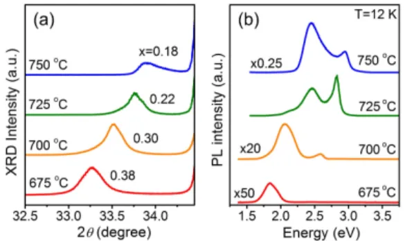
Figure 1 (a) shows the XRD θ−2θ scans for the InxGa1−xN films around the (0002) diffraction
peaks. By lowering the growth temperature (Tg) from 750 to 675 °C, the In composition x
reported in Ref. 20. In Fig. 1(b), the corresponding PL spectra measured at T =12 K are displayed. A redshift in the PL emission band in accordance with the increasing In composition in the InGaN films can be seen. Besides, for samples grown at Tg
≥
700
°C, thePL emission bands exhibit double peaks. Such a double PL peak feature was usually attributed to the presence of quantum-dot-like or phase separated In-rich regions in InGaN films due to spinodal decompositions [28,29]. However, significant phase separation is not expected in the investigated InGaN films, since no multiple XRD peak was resolved in the
2
θ− θ scans. An alternative interpretation is the occurrence of discontinuous strain relaxations when the InGaN layer exceeds the critical thickness, resulting in two PL peaks originated from a strained and a nearly fully relaxed regions located at different depths of the film [12].
Fig. 1. (a) X-ray diffraction and (b) PL spectra of InGaN films grown at different temperatures from 675 to 750 °C.
To clarify the origin of the double PL peaks, reciprocal space mappings (RSM) of the InGaN films by high-resolution XRD of an asymmetric plane (105) have been performed, which are shown in Fig. 2. The analysis of XRD RSM for InGaN/GaN layers has been detailed in Pereira et al. [30]. It provides information on both the in-plane a and out-of plane
c lattice constants, so that the In composition x including the strain state of the InGaN films
can be extracted. According to Ref. 30, we plot vertical and slanted dashed lines in Figs. 2(a) to 2(d), which represent the strain and the relaxation lines for the InGaN film, respectively. The full lines connecting the strain and relaxation lines are isocomposition lines. For the 675 °C-grown InGaN film, only one diffraction peak on the relaxation line can be observed, indicating that the strain in the InGaN film has been fully relaxed. However, for InGaN films grown at Tg
≥
700
°C, the diffraction profile becomes asymmetric and elongated betweenthe strain and relaxation lines, indicative of an inhomogeneous strain distribution in the InGaN film. The maximum of the diffraction profile shifts gradually from the relaxation line to the strain line with increasing Tg. From the measured asymmetric diffraction profile, the
InGaN film can be considered as a mixture of the strained [InGaN(S)] and the relaxed [InGaN(R)] phases.
Fig. 2. Reciprocal space mapping of InGaN films grown at (a) 675 °C, (b) 700 °C, (c) 725 °C, and (d) 750 °C.
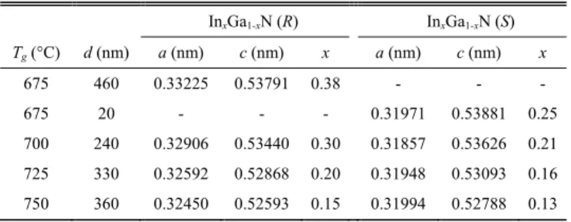
According to the measured lattice constants of the strained and relaxed phases, we can deduce the In composition x of different strain states, which are listed in Table 1. In all samples, the In composition of the relaxed phase is higher than that of the strained phase. This can also be seen from the RSMs shown in Fig. 2, where the asymmetric diffraction profiles are extended continuously between two isocomposition lines, indicative of a composition gradient in the film. Such a variation of In composition can be attributed to the compositional pulling effect, which has been reported in Ref [31,32]. The strain exhibit in the InGaN epilayer was considered as the main driven force, which tends to expel In atoms from the epilayer during the initial stage of InGaN growth. As the growth proceeds, the strain in the InGaN layer relaxes gradually, leading to the incorporation of more In atoms into the subsequent InGaN layer. From Table 1, we also find that the difference in the In compositions of the two phases also increases with the In composition. This further confirms that the strain is the main cause of the compositional pulling effect [32].
Table 1. Thickness d, Lattice Constants a and c, and In Composition x of InGaN Films Grown at Different Growth Temperatures Tg
InxGa1-xN (R) InxGa1-xN (S) Tg (°C) d (nm) a (nm) c (nm) x a (nm) c (nm) x 675 460 0.33225 0.53791 0.38 - - - 675 20 - - - 0.31971 0.53881 0.25 700 240 0.32906 0.53440 0.30 0.31857 0.53626 0.21 725 330 0.32592 0.52868 0.20 0.31948 0.53093 0.16 750 360 0.32450 0.52593 0.15 0.31994 0.52788 0.13
According to the structural analysis, we conclude that the observed double PL peaks are associated with both the strain relaxation and the compositional pulling effect in the InGaN films. The higher (lower) energy PL peak can be attributed to the emission from the strained (relaxed) phase in the InGaN film. For the sample grown at Tg = 675 °C, only the relaxed
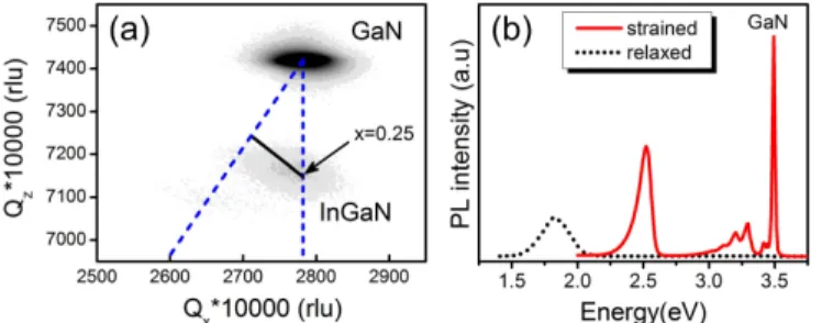
phase and one PL peak were observed. To verify the PL peak assignments, we have also grown an InGaN film at 675 °C with a nominal thickness d<20 nm. From the RSM of the
thin InGaN film shown in Fig. 3(a), only the strained phase with x=0.25 is observed. As shown in Fig. 3(b), the PL peak of the strained InGaN film blueshifts to 2.52 eV, significantly higher than the relaxed film at 1.82 eV. This further confirms that double PL peaks are originated from the strained and relaxed phases in the InGaN films.
The double PL peak feature associated with the strained relaxation in InGaN films has been well studied by Pereira et al. [12,33]. It has been established that the PL peak splitting (ΔE) is linearly correlated with the in-plane strain (εxx) at the InGaN-GaN interface, which
was found to be associated with a transition from a planar (2D) to a Stranski–Krastanow-like (2D–3D) growth mode [33]. According to the atomic force microscopy analyses, our InGaN films also show a 3D-like surface morphology with a surface roughness (rms) in the range of 20-60 nm, in agreement with Pereira et al. [33]. However, the PL peak splittings ΔE of our samples are about two times larger than that reported in Ref. 33. It should be noted that the universal linear dependence between ΔE and εxx was based on the approximation that the In
composition is uniform along the growth direction. The larger PL splitting observed here thus further confirms that the compositional pulling effect is significant in our InGaN films grown by the two-heater scheme.
Fig. 3. (a) RSM of d < 20 nm InGaN film grown at 675 °C. (b) PL spectra of InGaN films with different thickness grown at 675 °C.
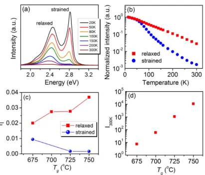
The optical properties of the double PL peaks associated with the strain relaxation in the InGaN films have been investigated by temperature-dependent PL measurements. Figure 4(a) shows the temperature evolution of PL spectrum for the InGaN film grown at 725 °C. The corresponding integrated PL intensities as a function of temperature for both phases are displayed in Fig. 4(b). The PL intensity of the strained phase decreases more rapidly with increasing temperature when T >80 K. At room temperature (RT), the PL spectrum is dominated by the emission from the relaxed phase. Figure 4(c) shows the ratio of the integrated PL intensity at RT to that at T=12 K, η =IPL(300 K) /IPL(12 K) for all samples (except for the strained phase of the 700 °C grown sample, which shows vanished PL intensity at RT). It is evident that the emission efficiency for the relaxed phase is better than the strained phase, regardless of different growth temperatures. However, we noted that the PL efficiency of the InGaN films degraded with decreasing Tg. This is evident from the RT
PL intensity for all the investigated samples shown in Fig. 4(d), where the PL intensity decreases by over 3 orders of magnitude as Tg was decreased from 750 to 675 °C. It is well
known that growth temperature plays a decisive role in the growth of In-rich InGaN. Although a lower Tg can incorporate more In composition into the InGaN film, it is usually
Fig. 4. (a) Temperature-dependent PL of InGaN film grown at 725 °C. (b) Integrated PL intensity as a function of temperature for both phases. (c) Emission efficiency (η) of both phases and (d) RT PL intensity of relaxed phase as a function of Tg.
It is worth to point out that the relaxed phases have superior PL efficiency than the strained phases at RT seem to be counterintuitive, since the relaxed phases are expected to be more dislocated. To clarify this unusual character, we have performed time resolved-PL measurements. Figure 5(a) shows the PL decay traces measured at 12 K for the strained and relaxed phases in the InGaN film grown at 750 °C. The decay traces for both phases show a non-single exponential decay, which was commonly observed in the In-containing alloys due to the carrier localization effect. The slower PL decay for the relaxed phase can be attributed to a more pronounced localization effect in the relaxed phase due to alloy disorders. In Fig. 5(b), the effective PL decay lifetimes (τeff at which the PL intensity decreased to 1/e) of the
strained and relaxed phase for all samples are displayed. The measured τeff for the relaxed
phase decreases with decreasing Tg, while the measured τeff for the strained phase is nearly
unchanged at about 1 ns for all samples. For the relaxed phase, the decreasing τeff with the
decreasing Tg may arise from the higher defect density formed in the relaxed layer grown at
lower temperatures.
Fig. 5. (a) TRPL spectra measured at 12 K and (b) the effective carrier lifetimes deduced from decay traces for both phases as a function of Tg.
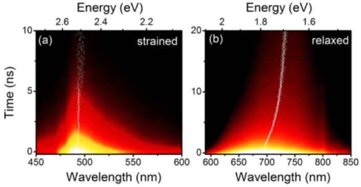
The effect of carrier localization can be further investigated by energy-dependent TRPL measurements. In Figs. 6(a) and (b), the time-evolution PL spectra for the strained and relaxed phases in the InGaN film grown at 675 °C are displayed. A clear temporal PL redshift is observed for the relaxed phase. Such a temporal redshift have been observed in InGaN alloys due to the carrier transfers from localization centers with higher energies to those with lower energies [34]. On the contrary, the temporary PL redshift is absent in the strained phase. Similar behaviors have also been observed in samples grown at higher temperatures. Therefore, we conclude that the carrier localization effect is more pronounced in the relaxed phase. This trend can also be explained by the compositional puling effect caused by strain relaxations, leading to inhomogeneous In distribution and the formation of local In-rich regions in the relaxed phase.
Fig. 6. Energy-dependent TRPL of InGaN films grown at 675 °C for (a) strained phase and (b) relaxed phase.
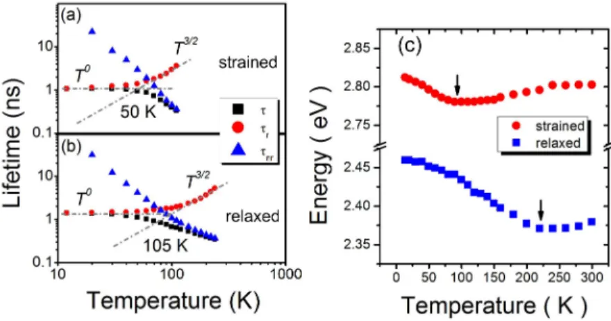
Carriers confined in localization centers, which prevent the carrier diffusions to nonradiative recombination centers, could be the main cause of the superior PL efficiency associated with the relaxed phases at RT. This assertion can be verified by temperature-dependent TRPL measurements. Figures 7(a) and 7(b) shows the measured decay time τ as a function of temperature for the strained and relaxed phases in the InGaN film grown at 725 °C. The measured ( )τ T can be decomposed into the radiative lifetime τr and the nonradiative lifetime τnr according to 1/τ=1/τr +1/τnr. A standard way to extract τr and
nr
τ from the measured ( )τ T is to determine the radiative efficiency ( )η T =τnr/ (τ τr+ nr) according to the measured temperature-dependent PL intensity η( )T =IPL( ) /T IPL(12 K), by
which the radiative and nonradiative lifetimes can be determined. The deduced τr and τnr are also shown in Fig. 7. For the strained phase, the deduced τr is nearly constant at temperatures
below 50 K, but above which it exhibits a T3/ 2 dependence. The radiative lifetime for a direct
band-gap material is related to the effective densities of states in the conduction or valence bands [35], which can be simplified to a temperature dependence of Td/ 2, where d is the
system dimensionality. For T >50 K with d≈3 can be attributed to the recombination processes in bulk materials, while for T <50 K with d≈0 could arise from the 0-D like transition due to the localizations of carriers in In-rich regions. For the relaxed phase, the effect of carrier localization is more pronounced, which is evident from the higher turning temperature at around 105 K. The effect of carrier localization can be further examined by the temperature dependent PL peak energy shift, as shown in Fig. 7(c). Both the strained and relaxed phases show “S-shaped” energy shift, indicative of carrier localizations. The relaxed phase also exhibits a higher turning temperature in the S-shaped energy shift, in agreement with the time-resolved PL analysis shown in Figs. 7(a) and 7(b). This further verifies that carrier localizations are more pronounced in the relaxed phase, leading to the superior emission properties at RT than the strained phase in InGaN films.
Fig. 7. The measured decay time τ as a function of temperature T for (a) the strained phase and
(b) the relaxed phase of the InGaN film grown at 725 °C. The deduced radiaive τr(T) and
nonradiative τnr(T) lifetimes are also shown. (c) The PL peak energies of the strained and
relaxed phases as a function of temperature for the same sample.
4. Conclusions
Optical properties of thick InxGa1−xN layers with x ranging from 0.13 to 0.38 are investigated
by PL and time-resolved PL measurements. The inhomogeneous strain distribution and In composition in the InGaN films are studied by high resolution XRD and RSM along an asymmetric axis. PL results together with RSMs indicate that the observed double PL peaks are associated with the strained and relaxed phase in the InGaN films. It is evident that the better emission efficiency in relaxed phase than the strained phase from the temperature-dependent PL measurements. Recombination dynamics from time-resolved PL measurements reveal that the carrier localization effect is more pronounced in the relaxed phase. Finally, we conclude that the emission efficiency is strongly correlated with the localization effect in thick InGaN films.
Acknowledgments
This work was supported in part by the program of MOEATU and the National Science Council of Taiwan under Grant No. NSC-101-2628-M-009-002-MY3.