128 IEEE TRANSACTIONS ON COMPONENTS AND PACKAGING TECHNOLOGY, VOL. 23, NO. 1, MARCH 2000
Effect of Bottom Electrodes on Resistance
Degradation and Breakdown of (Ba, Sr)TiO
3
Thin
Films
M. S. Tsai and T. Y. Tseng, Senior Member, IEEE
Abstract—The influence of bottom electrodes (Pt, Ir, Ru) on the degradation of (Ba,Sr)TiO3(BST) thin films under dc stress condi-tions was investigated. The current-time ( – ) and current–voltage ( – ) measurement results indicated that the BST thin films de-posited on Ru have faster degradation than those dede-posited on Pt and Ir. The degradation was considered to be caused by the dete-rioration of Schottky-barrier. Under dc stress conditions, the di-electric relaxation current in the BST didi-electric films probably en-hances the deterioration. The breakdown time was found to be ap-proximated by an exponential function of an electric field[ =
exp( )] for dc stress. The value of the exponential factor for BST deposited on Pt and Ir was about a quarter of that for BST deposited on Ru. The different value of observed under dc stress indicates that the degradation of BST on Ru would be more serious than on Pt and Ir. The ten years lifetime of time-dependent dielec-tric breakdown (TDDB) studies indicate that BST on Pt, Ir and Ru have longer lifetime over ten years on operation at the voltage bias of 1 V.
Index Terms—Bottom electrodes, BST thin films, degradation, dielectric film, dynamic random-access memories, sputtering.
I. INTRODUCTION
T
HE (Ba,Sr)TiO (BST) dielectric film has attracted great attention for practical use in a capacitor of giga-bit dy-namic random-access memories (DRAM’s) because of its high dielectric constant, low leakage current density, high dielectric breakdown strength, paraelectric perovskite phase that does not exhibit fatigue, aging and the ease of composition control [1], [2]. The electrical characteristics of BST thin films greatly de-pend on the deposition conditions (sputtering power, substrate temperature, sputtering ambient, gas pressure etc.) [3]–[7], the composition of the BST thin films [8], [9], the bottom elec-trode materials [10]–[12], e.g., Pt, Pt/Ta, Pt/TiN/Ti, Pd/Ti, Pd, etc., post-annealing condition [5], [13]–[15], and the electrical degradation and breakdown for ceramics of perovskite-type ti-tanate [16]–[18]. In these BST materials, a dc stress causes re-sistance degradation, characterized by a slow increase of the leakage current after a characteristic time. The resistance degra-dation of BST films is characterized by extreme lowering of the resistance when simultaneous temperature and dc field stress areManuscript received June 1, 1999; revised December 1, 1999. This paper was recommended for publication by Associate Editor M. Braunovic upon evalua-tion of the reviewers’ comments. This work was supported by the Naevalua-tional Sci-ence Council, R.O.C., under Project NSC 86-2112-M009-028.
M. S. Tsai is with the Mosel Vitelic Company, Hsinchu, Taiwan, R.O.C. T.-Y. Tseng is with the Department of Electronics Engineering and Institute of Electronics, National Chiao Tung University, Hsinchu, Taiwan 30050, R.O.C.
Publisher Item Identifier S 1521-3331(00)01914-0.
applied to the films. The degradation process limits the lifetime and reliability of BST capacitors. There is a constant bias on the capacitor dielectrics in both DRAM and on-chip capacitor applications, as a consequence, it is worth studying their degra-dation under static dc stresses. Many parameters, such as doping [18], stoichiometry [16], grain size [17] and electrode properties affect the degradation. Thus, it is important to evaluate such in-stabilities in case of BST thin films, for its applications. In this work, we investigate the effect of bottom electrodes (Pt, Ir, Ru) on the resistance degradation and breakdown of BST thin films. A qualitative explanation for BST breakdown based on band di-agram is presented.
II. EXPERIMENTAL
BST thin films were deposited on metals/SiO /(100)Si (metals are Pt, Ir, and Ru) bottom storage node electrodes by rf magnetron sputtering. The detailed deposition conditions of the BST thin films on various bottom electrodes were described in reference [19], [20]. The BST targets with a diameter of 3 in and a thickness of in were synthesized using standard solid-state reaction process. The sputtering chamber was evacuated to a base pressure of torr. All films were prepared at fixed power of 100 W (power density is 2.26 W/cm ) and constant pressure of 10 mtorr which was maintained by a mixture of 50% Ar and 50% O2(oxygen flow
mixing ratio O /(O Ar) (OMR) is 50%) with a total flow of 20 sccm. All of the BST films have the same thickness of around 80 nm. The substrate temperature of the sputtered BST films was at 500 C. The composition of sputtered films was Ba/Sr on the basis of ICP analysis. The BST thin films were post-annealed at temperatures ranging from 500 to 700 C in O atmosphere using a quartz glass tube furnace (FN) for 20 min. Then, the 50 nm thick top Pt electrodes with diameters of 165, 255, and 350 m were formed by sputtering and patterned by the shadow mask process.
The film thickness was determined from ellipsometry. The structure was characterized by X-ray diffraction (XRD, Siemens D5000). Depth profiles of oxygen near the inter-face of BST/bottom electrodes were analyzed by secondary ion mass spectrometry (SIMS, CAMECA IMS-4f). The capacitance–voltage ( – ) characteristic was measured on the metal-insulator-metal (MIM) structure by measuring the capacitance at 100 KHz as a function of a swept posi-tive-to-negative voltage bias. Dielectric constant of the films was calculated from the capacitance measured at 100 KHz
TSAI AND TSENG: EFFECT OF BOTTOM ELECTRODES ON RESISTANCE DEGRADATION AND BREAKDOWN OF (Ba, Sr)TiO3THIN FILMS 129
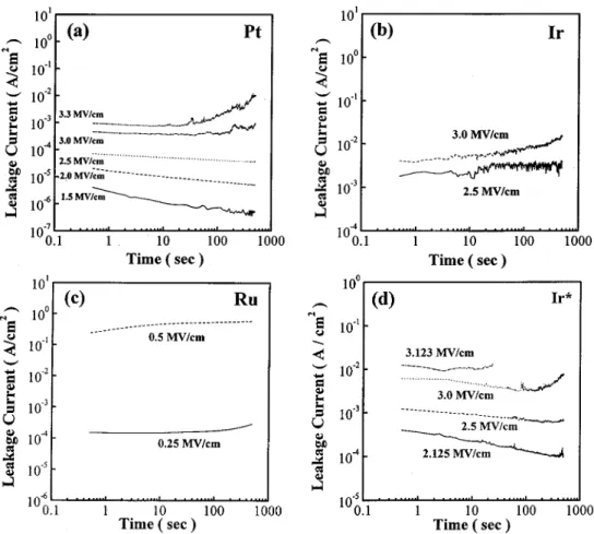
Fig. 1. Leakage current-stress time properties of BST films deposited at 500 C on (a) Pt, (b) Ir, (c) Ru, and (d) Ir* under different dc stress fields.
without bias voltage. The dielectric properties were measured as a function of frequency with a Hewlett-Packard (HP) 4194A impedance-gain phase analyzer. The current–voltage ( – ) and current–time ( – ) measurements were performed by measuring the current through the sample with a HP4145B. And the leakage current at positive bias, the electrons flow from bottom electrode to top electrode.
III. RESULTS ANDDISCUSSION
The bottom electrode had a pronounced effect on the dielec-tric constant and the leakage current density of the BST films measured at 100 kV/cm with delay time 30 s. The dielectric con-stant and leakage current of the films were also strongly depen-dent on the post-annealing conditions. BST thin film deposited on Ir bottom electrode at 500 C, after 700 C annealing in O for 20 min, has the dielectric constant of 593, a loss tangent of 0.019 at 100 kHz, a leakage current density of
A/cm at an electric field of 100 kV/cm with a delay time of 30 s, and a charge storage density of 53 fC/ m at an applied field of 150 kV/cm [19]. The BST films deposited on Ir with post-annealing can obtain better dielectric properties than on other bottom electrodes in our experiments. And Ru electrode is unstable because the interdiffusion of Ru and Ti is occurred at the interface between the BST and Ru after post-annealing [19], [20]. The leakage current of BST thin films was expected to be affected by the contact potential barrier and polarization loss. The BST films deposited on Pt, Ir, IrO /Ir, and RuO /Ru
after post-annealing were stabler than BST on Ru. The details were given in reference [19], [20].
Fig.1(a)–(d) show that the – characteristics of BST de-posited on Pt, Ir, Ru, and Ir* (BST on Ir annealed at 600 C for 20 min in O ambient after deposition) under different dc stress field. The responses are substantially the same as those reported by Waser for SrTiO thin films with a thickness of 200 nm [21]. Fig. 1(a) shows that the leakage current of BST deposited on Pt under 1.5, 2.0, and 2.5 MV/cm dc stress fields slowly decreased with stress time. And the leakage current of BST deposited on Pt under 3.0 and 3.3 MV/cm dc stress fields slowly decreased with stress time in the beginning stage of the stress, and then the current stopped decreasing further, and gradually increased up to the breakdown. For a field less than 2.5 MV/cm, only slow decrease of current without any significant current degra-dation was observed within the measured time range. Fig. 1(b) indicates that the leakage current of BST deposited on Ir under 2.5 and 3.0 MV/cm dc stress fields slowly increased with stress time. Fig. 1(c) shows that the leakage current of BST deposited on Ru under 0.5 MV/cm dc stress field slowly increased with stress time. And the leakage current of BST deposited on Ru under 0.25 MV/cm dc stress field slowly decreased with stress time in the beginning stage of the stress, and then the current stopped decreasing further, and gradually increased up to the breakdown. For a field less than 0.25 MV/cm, only slow decrease of current with a very small current degradation was observed within the measured time range. From the leakage current versus stress time data, the BST thin film deposited
130 IEEE TRANSACTIONS ON COMPONENTS AND PACKAGING TECHNOLOGY, VOL. 23, NO. 1, MARCH 2000
Fig. 2. SIMS profile of BST deposited on (a) Ir, (b) Ir after 600 C, O annealing.
on Pt has the smaller resistance-degradation and the BST thin film deposited on Ru has the larger resistance-degradation. Fig. 1(d) shows that the leakage current of BST deposited on Ir* under 2.125 and 2.5 MV/cm dc stress fields slowly decreased with stress time, and then the current slightly increased around 500 s. And the leakage current of BST deposited on Ir* under 3.0 and 3.123 MV/cm dc stress fields slowly decreased with stress time in the beginning stage of the stress, and then the current stopped decreasing, and gradually increased up to the breakdown. For fields less than 2.5 MV/cm, slow decrease of current with less current degradation was observed within the measured time range. The leakage current versus stress time data show that the BST thin film deposited on Ir* has the less resistance degradation than the BST on Ir, because of the formation of IrO at the interface of BST and Ir* will suppress the accumulation of oxygen vacancy [20] and hence the degradation caused by the deterioration of Schottky-barrier would be smaller than those on Ir.
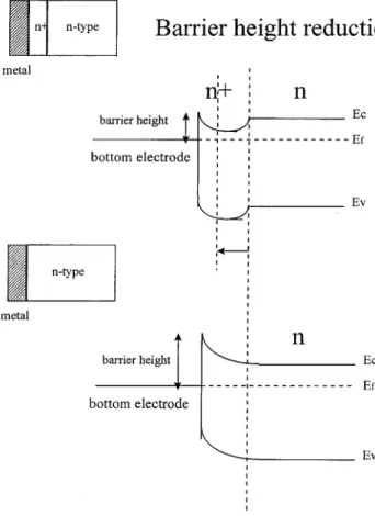
For understanding the effect of annealing on the dielectric properties and reliability of the BST on Ir bottom electrodes, we compare SIMS data of BST films before and after an-nealing [Fig. 2(a) and (b)]. From SIMS data, we observed that the oxygen concentration at BST/Ir* interface is larger than the oxygen concentration at BST/Ir interfaces, as shown in Fig. 2(a) and (b). The Ti and Ir profiles of BST on Ir remain the same but the oxygen concentration at the interface slightly increases, that is, a IrO layer is probably formed. Fig. 3 is provided for further explaining the effect of the change in the interface due to annealing on the properties of BST films. The thinner interfacial layer of IrO are suggested to suppress the
Fig. 3. Barrier height of “metal-n type-n type” and “metal-n type” structures.
accumulation of the oxygen vacancies at the BST/Ir interface. Therefore, the interface of the BST/Ir has reduced accumula-tion of oxygen vacancies after post-annealing. The BST film tends to show an -type conductivity because the oxygen vacancy acts as a donor dopant. The higher concentration of oxygen vacancy accumulated at the interface tends to show an n -type conductivity (Fig. 3). Hence, the BST/Ir structure before post-annealing are similar to the “metal-n type-n type” structure whereas those after post-annealing are similar to the “metal-n type” structure. On the basis of the point of view of the physics of semiconductor devices, the “metal-n type-n type” structure will result in barrier height reduction, which leads to larger barrier height occurred in the “metal-n type” structure, as shown in Fig. 3. Therefore, the leakage current of BST on Ir after post-annealing decreases with the annealing temperature [19], [20], because the barrier height of BST on Ir after post-annealing increases with the annealing temperature. The reliability of BST on Ir were further improved by post-deposition annealing in O at 600 C for 20 min.
The leakage current versus time of BST films under different dc stress is shown in Fig. 1. The leakage current decreased with stress time under “low dc stress field” (no degradation) which is called the charging current [22]. The leakage current gradu-ally increased up to the breakdown under “high dc stress field” (with degradation), because that the migration and creation of oxygen vacancies under high dc stress field would occur and the oxygen vacancies migration toward the cathode and pilling up of oxygen vacancies near the cathode certainly lower the resistance
TSAI AND TSENG: EFFECT OF BOTTOM ELECTRODES ON RESISTANCE DEGRADATION AND BREAKDOWN OF (Ba, Sr)TiO3THIN FILMS 131
Fig. 4. Leakage current-electric field properties of BST films deposited at 500 C on (a) Pt, (b) Ir, (c) Ru, and (d) Ir* under different dc stress fields with 500 s.
of the Schottky junction which would increase the leakage cur-rent. The resistance degradation can be better understood from the band diagram of BST thin films, which will be described in Fig. 9.
Fig. 4(a)–(d) depict that the leakage current with delay time 30 s of BST deposited on Pt, Ir, Ru, and Ir* bottom electrodes, under different stress field with 500 s. Fig. 4(a) shows that the leakage currents of BST on Pt under 1.5, 2.0, and 2.5 MV/cm stress fields have no degradation and leakage current degradation has already occurred in the film after 3.0 and 3.3 MV/cm stress fields. Fig. 4(b) shows the larger degradation on the leakage currents of BST on Ir under 2.5 and 3.0 MV/cm stress fields. Fig. 4(c) indicates that the leakage currents of BST on Ru under 0.25 MV/cm stress field have no degradation and leakage current degradation has already occurred in the film after 0.5, 1.06, and 1.17 MV/cm stress fields. This is (Fig. 4) in good agreement with the results shown in Figs. 1 and 8. Fig. 4(d) shows that the leakage currents of BST on Ir* under 2.125 MV/cm have only slight degradation. The BST on Ir* under 2.5 and 3.0 MV/cm stress fields have degradation of leakage current and it is smaller than those on Ir. Therefore, the electrical characteristics (e.g., high dielectric constant and low leakage current) and reliability of BST on Ir were further improved by post-deposition annealing in O at 600 C for 20 min. The details were given in the analysis of Figs. 1–3.
Fig. 5 indicates that the characteristic time is dependent on the electric field. The characteristic time is defined as
Fig. 5. Characteristic time(t ) is dependent on the electric field.
the time when the current density shows a value larger than the minimum by one order under dc stress. The character-istic time increased with the decrease of the electric field. The BST on Pt, Ir, and Ir* have longer characteristic times than those on Ru, hence the BST thin film deposited on Pt, Ir, and Ir* has the smaller resistance-degradation and the BST thin film deposited on Ru has the larger resistance-degradation. The results indicated in Fig. 5 have a good agreement with the re-sults shown in Figs. 1, 4, and 8. This phenomenon implys that the Schottky-barrier of BST might be affected by dc stress. The higher Sckottky-barrier has the less resistance-degradation (The difference in work functions which are, respectively, 5.6, 5.35,
132 IEEE TRANSACTIONS ON COMPONENTS AND PACKAGING TECHNOLOGY, VOL. 23, NO. 1, MARCH 2000
Fig. 6. Leakage current–electric field properties of BST films deposited at 500 C on (a) Pt, (b) Ir, and (c) Ru under different measurement temperatures.
and 4.8 eV for Pt, Ir, and Ru). Hence, BST on Pt has less re-sistance-degradation and long characteristic time. And also the BST on Ir* has less resistance degradation than the BST on Ir. The resistance degradation can be better understood from the band diagram of BST thin films, which will be described in Fig. 9.
Fig. 6(a)–(c) show that the leakage current with delay time 30 s of BST, deposited on Pt, Ir and Ru bottom electrodes at 500 C with 50% OMR with Pt top electrode, under different measurement temperatures. The asymmetry of leakage current exists [19], [23], because the potential barrier formed at the in-terface between the top electrode and BST is not as high as that at the interface between bottom electrode and BST [19], [23]. The leakage currents at positive bias of BST on Pt have a little change at various temperatures [Fig. 6(a)]. However, the leakage currents at positive bias of BST on Ir have more changes at var-ious temperatures (espectially at 150 C) than those of BST on Pt [Fig. 6(b)]. The leakage currents at positive bias of BST on Ru have the most significant changes at various temperatures among three different bottom electrodes. The results show that the Schottky-barrier of BST might be affected by temperature and the BST thin film deposited on Pt would have the smaller re-sistance-degradation for thermal breakdown (temperature) and the BST thin film deposited on Ru would have the larger resis-tance-degradation for thermal breakdown.
Fig. 7. Characteristic time(t ) is dependent on the temperature.
Fig. 7 illustrates the Arrhenius plot of the resistance degra-dation for the BST thin films deposited on Pt, Ir, Ir*, and Ru. The characteristic time is dependent on the temperature and shows a linear behavior, well fitted by the Arrhenius
equa-tion; , where is the overall coefficient,
Ea the activation energy, the Boltzmann constant and the ab-solute temperature. The decreased with the increase of the temperature. The activation energies of the BST deposited on
TSAI AND TSENG: EFFECT OF BOTTOM ELECTRODES ON RESISTANCE DEGRADATION AND BREAKDOWN OF (Ba, Sr)TiO3THIN FILMS 133
Fig. 8. Time to breakdown of the BST films on various bottom electrodes as a function of stress field.
Pt, Ir and Ir* under 3.0 MV/cm stress are 0.478 eV, 0.477 eV, and 0.477 eV, respectively. The activation energy of the BST deposited on Ru under 1.14 MV/cm is 0.392 eV. The BST on Pt showed longer of the degradation at the same bias and temperature. The BST on Pt, Ir, and Ir* exhibited longer than that on Ru at the same temperature. The results demon-strate that the BST capacitors on Pt, Ir, and Ir* have less dete-rioration of resistance to dc voltage stress compared to that on Ru at elevated temperatures. The results shown in Figs. 6 and 7 are in good agreement. It has been reported that the activa-tion energy of the 18% OMR BST deposited on Pt at 650 C is 0.8 eV at 100 kV/cm [23], which is different from our data 0.478 eV at 3.0 MV/cm. This difference might be attributed to the differences in grain size and stoichiometry between films fabricated at various processing conditions [24]. The activation energy 0.478 eV at 3.0 MV/cm indicates much less temperature sensitivity than the 0.8 eV at 100 kV/cm [24], hence our film has less deterioration of resistance to dc voltage stress at elevated temperatures than that reported in reference. The grain size of BST deposited on Ru has a larger value of 18 nm, while that of BST on Pt and Ir has the smaller values of 7 nm and 12 nm. The resistivity of BST deposited on Ru has a smaller value of 7 M -cm, while that of BST on Pt and Ir has the larger values of 24 M -cm and 20 M -cm. Hence, the BST capacitors on Pt, Ir, and Ir* have less deterioration of resistance to dc voltage stress compared to that on Ru at elevated temperatures.
Fig. 8 shows that the breakdown time under a given dc stress for BST thin films deposited on the different bottom electrodes, which predicts the ten year lifetime at 1 V operating voltage. It indicates that the BST films on Pt, Ir, and Ir* have a longer lifetime than the BST on Ru. We can describe the breakdown time, , of each film in terms of the empirical equation
(1) where is preexponential factor, exponential factor, and electric field. On the basis of the results shown in Fig. 8, the values of at room temperature are estimated to be
, and s for BST thin films deposited on Pt, Ir, Ir*, and Ru, respectively. And the values of at room temperature are estimated to be 2.33, 2.37, 2.36, and
8.9 cm/MV for BST films on Pt, Ir, Ir*, and Ru, respectively. From the estimated data , the BST films deposited on Pt, Ir, and Ir* have a longer lifetime at lower operating voltage than that on Ru. The values of for BST on Pt, Ir, and Ir* are about a quarter of that for BST on Ru. The different value of observed under dc stress indicates that the degradation of BST on Ru would be more serious than on Pt, Ir, and Ir*, which is in good agreement with the results shown in Figs. 1–7. It has been reported in [25] that the value of at 27 C for BST on Ir was evaluated to be 2.5 cm/MV, which is resonably close to our value. Tsai et al. [23] assumed that the main conduction in the BST thin films deposited at higher OMR (40%–60%) is the thermionic emis-sion of electrons from cathode electrode into the BST thin film (Schottky emission). Therefore, the Schottky interface-barrier would influence the characteristics. The time-dependent dielectric breakdown (TDDB) as shown in Fig. 8 is also refered as resistance degradation of dielectrics which shows a slow in-crease of leakage current under dc field stress, hence it is con-sidered that the degradation of BST films was caused by the de-terioration of Schottky interface-barrier. On the other hand, the polarization enhanced electron transport (dielectric relaxation current) under long-time dc stress would also cause the decrease of the values of interface-barrier height and the depth of the trap center level [23]. Under dc stress conditions, the dielectric re-laxation current in the BST dielectric films probably enhances the deterioration.
The theories proposed for explaining the degradation mecha-nism of perovskite titanates may include two major categories: grain boundary model and reduction model [18]. In the grain boundary model, a dc field induced deterioration of the grain boundaries is responsible for the degradation phenomenon. The model assumes that the grain in dielectric ceramics is a resistor C and the grain boundary is a thin insulating layer R. There are many of RC series equivalent circuit in paralled throughout the ceramic. Based on the equivalent circuit analysis it indicates the grain boundary plays a prominent role in the degradation of the ceramics. Higher breakdown strength is obtained with decreasing grain size. In the case of the reduction model, the positively charged oxygen vacancies with relative high mobility electromigrate toward the cathode under dc electric field. The oxygen vacancies then pile up at the front of cathode and are compensated by the electron injected from cathode. On the other hand, at the anode, an electrode reaction leads to generation of oxygen gas and electrons, leaving oxygen vacancies behind, and may cause an oxidation of electrode material. The reduction reaction leads to a growth of n-conducting cathodic region to-ward the anode, and to an increase of the electronic conductivity. The net result is that the space charge accumulation at grain boundaries and interface of BST and metal reduces the grain boundary height and interface barrier height, and increase the leakage current. The experimental results in our study are related to the grain boundary model and reduction model: 1) the BST on Pt has more “grain boundaries” than BST on Ru because the grain size of BST on Pt is smaller [19], therefore, the BST on Pt is expected to have longer life-time on the basis of grain boundary model, which was verified by the result indicated in Fig. 8, 2) the BST on Pt has higher “interface barrier” than BST on Ru, as the work function of Pt is larger than that of Ru. It is considered that
134 IEEE TRANSACTIONS ON COMPONENTS AND PACKAGING TECHNOLOGY, VOL. 23, NO. 1, MARCH 2000
the degradation in our samples was largely caused by the dete-rioration of Schottky-barrier. On the basis of reduction model, this deterioration due to the accumulation of oxygen vacancies at the interface which reduces the barrier height and increase the leakage current. Therefore, the experimental result shows that the BST on Pt processing higher Schottky-barrier have less degradation, which is in accordance with the reduction model, and 3) the polarization enhanced electron transport in BST film on Ru is predicted to be more serious than that of BST on Pt because the polarization of BST on Ru is higher than that in BST on Pt [19]. The effect of space charge (oxygen vacancy) accumu-lation at grain boundaries leading to reduce the grain boundary height and increase the leakage current is expected to be smaller here, because the 50% OMR BST employed in the present study has been reported to contain little oxygen vacancies [23]. Hence, the BST film on Pt has smaller degradation and longer life-time, and the BST on Ru has more degradation and shorter life-time. And the degradation of BST on Ir is between the BST/Pt and BST/Ru, because the number of grain boundaries, interface barrier height and polarization enhanced electron transport (relaxation current) of BST on Ir are between the BST/Pt and BST/Ru. The dielectric constant and leakage current of BST on Ir were further improved by post-deposition annealing in O at 600–700 C for 20 min [20]. The TDDB life-time of BST on Ir* exhibit better reliability under long-term electrical stress than that on Ir. The formation of IrO in the interface of BST and Ir* can suppress the accumulation of oxygen vacancy, thus reducing the deterioration of Schottky-barrier and the degradation.
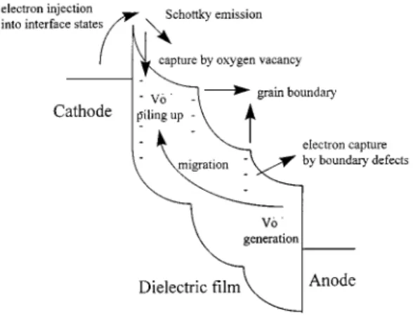
Among various conduction mechanisms related to the current flow through a dielectric film under a dc applied stress, we pro-pose that Schottky emission can explain our results better, since the net current across the dielectric is usually more sensitive to electrode materials. Therefore, the Schottky current is the dom-inant current for the field region considered, although barriers formed in grain boundaries probably also affect the carrier con-duction. For the BST films used in this work, the decrease of the resistance in the Schottky barrier between the cathode (bottom electrode) and the dielectric seems to be the main cause of the re-sistance degradation, in accordance with the conduction mecha-nism. We deduce a flatband model for metal-BST-metal system. Fig. 9 shows the energy band after contact and the creation and migration of defects, such as oxygen vacancies. The symbol “-” represents the oxygen vacancy accumulation at interface. The BST film on Pt has a large area of grain boundaries due to small grain size, and the grain boundaries would depress the oxygen vacancy migration which leads to the formation of the -con-ducting region [18]. The barrier height in the interface of BST/Pt is larger such that there is higher resistance of the deterioration of Schottky-barrier. However, under a relatively high field, the migration and pilling up of oxygen vacancies near the cathode certainly lower the resistance of the Schottky junction. Based on the energy band strucutre of the investigated metal-BST-metal system and the experimental data illustrated in Figs. 1–8, the work function of contact material, grain size of the film and the accumulation of oxygen vacancy at the interface should take into account for explaining the TDDB and dc degradation of BST films. Therefore, the empirical relation between dielec-tric breakdown time and elecdielec-tric field, , is
Fig. 9. Schematic of band diagram for BST thin film capacitor for explaining conduction and resistance degradation.
not able to be directly derived from the available degradation models of the deterioration of Schottky junction. The detailed study of migration and creation of defects, such as oxygen va-cancies, is suggested to be important for providing possible ex-planation about the resistance degradation phenomena of the BST films.
IV. CONCLUSION
We have demonstrated that the bottom electrodes appear to have a strong influence on the degradation and breakdown prop-erties of the BST thin films. The BST film deposited on Ru has faster degradation than those deposited on Pt, Ir, and Ir*. The relation between the breakdown times and the dc elec-tric field were well fitted by the empirical equation
. The value of the exponential factor for BST deposited on Pt, Ir, and Ir* was about a quarter of that for BST on Ru, which indicates that the degradation of BST on Ru would be more serious than on Pt, Ir, and Ir*. The BST film on Pt has longer lifetime than those on Ir, Ru, and Ir*, which was ascribed to smaller grain size, higher Schottky barrier, and less polariza-tion enhanced electron transport in the film on Pt.
REFERENCES
[1] Y. Ohno, T. Horikawa, H. Shinkawata, K. Kashihara, T. Kuroiwa, T. Okudaira, Y. Hashizume, K. Fukumoto, T. Eimori, T. Shibano, K. Ari-moto, H. Itoh, T. Nishimura, and H. Miyoshi, “A memory cell capacitor with Ba Sr TiO3(BST) film for advanced DRAMs,” in Proc. Symp.
VLSI Tech. Dig. Tech. Papers, 1994, pp. 149–150.
[2] T. Y. Tseng, “Fabrication and characterization of electroceramic thin films for semiconductor memory applications,” in Proc. Int. Electron
Devices Mater. Symp., vol. C25, 1996, pp. 89–96.
[3] T. Horikawa, N. Mikami, T. Makita, J. Tanimura, M. Kataoka, K. Sato, and M. Nunoshita, “Dielectric properties of (Ba,Sr)TiO3thin film
de-posited by RF sputtering,” Jpn. J. Appl. Phys., vol. 32, pp. 4126–4130, 1993.
[4] S. G. Yoon and A. Safari, “(Ba0.5,Sr0.5)TiO3thin film preparation by RF
magnetron sputtering and its electric properties,” Thin Solid Films, vol. 254, pp. 211–215, 1995.
[5] S. O. Park, C. S. Hwang, H. J. Cho, C. S. Kang, H. K. Kang, S. I. Lee, and M. Y. Lee, “Fabrication and electrical characterization of Pt/(Ba,Sr)TiO3/Pt capacitors for ultralarge-scale integrated DRAM
applications,” Jpn. J. Appl. Phys., vol. 35, pp. 1548–1552, 1996. [6] S. C. Sun, M. S. Tasi, P. Lin, J. A. Lay, D. C. H. Yu, and M. S. Liang,
“Effect of oxygen to argon ratio on properties of (Ba,Sr)TiO3thin films
prepared by Rf sputtering,” in Proc. ECS Meeting Abstr., vol. 96-1, Los Angeles, CA, 1996, pp. 184–185.
TSAI AND TSENG: EFFECT OF BOTTOM ELECTRODES ON RESISTANCE DEGRADATION AND BREAKDOWN OF (Ba, Sr)TiO3THIN FILMS 135
[7] M. S. Tsai, S. C. Sun, and T. Y. Tseng, “Effect of oxygen to argon ratio on properties of (Ba,Sr)TiO3thin films prepared by radio-frequency
mag-netron sputtering,” J. Appl. Phys., vol. 82, no. 7, p. 3482, Oct. 1, 1997. [8] E. Fujii, Y. Uemoto, S. Hayashi, T. Nasu, Y. Shimada, A. Matsuda, M.
Kibe, M. Azuma, T. Otsuki, G. Kano, M. Scott, L. D. Mcmillan, and C. A. Paz de Araujo, “ULSI DRAM technology with Ba0.7Sr0.3TiO3fillm
of 1.3 nm equivalent SiO2thickness and10 (A/cm2) leakage current,”
IEDM Tech. Dig., pp. 267–270, 1992.
[9] H. Kobayashi and T. Kobayashi, “Heteroepitaxial growth of quaternary Ba Sr TiO3thin films by ArF excimer laser ablation,” Jpn. J. Appl.
Phys., vol. 33, pp. L533–L536, 1994.
[10] W. J. Lee, I. K. Park, G. E. Jang, and H. G. Kim, “Electrical prop-erties and crystal structure of (Ba0.5,Sr0.5)TiO3thin films prepared on
Pt/SiO2/Si by RF magnetron sputtering,” Jpn. J. Appl. Phys., vol. 34,
pp. 196–199, 1995.
[11] K. Takemura, S. Yamamichi, P. Y. Lesaicherre, K. Tokashiki, H. Miyamoto, H. Ono, Y. Miyasaka, and M. Yoshida, “RuO2/TiN based
storage electrodes for (Ba,Sr)TiO3dynamic random access memory
capacitors,” Jpn. J. Appl. Phys., vol. 34, pp. 5224–5229, 1995. [12] T. Sakuma, S. Yamamichi, S. Matsubara, H. Yamaguchi, and Y.
Miyasaka, “Barrier layers for realization of high capacitance density in SrTiO3thin film capacitor on silicon,” Appl. Phys. Lett., vol. 57, pp.
2431–2433, 1990.
[13] Y. Fukuda, K. Numata, K. Aoki, and A. Nishimura, “Origin of dielectric relaxation observed for Ba0.5Sr0.5TiO3thin film capacitor,” Jpn. J. Appl.
Phys., vol. 35, pp. 5178–5180, 1996.
[14] C. S. Hwang, S. O. Park, H. J. Cho, C. S. Kang, H. K. Kang, S. I. Lee, and M. Y. Lee, “Deposition of extremely thin (Ba,Sr)TiO3thin films
for ultra large scale integrated dynamic random access memory applica-tion,” Appl. Phys. Lett., vol. 67, pp. 2819–2821, 1995.
[15] N. Ichinose and T. Ogiwara, “Preparation and rapid thermal annealing effect of (Ba,Sr)TiO3 thin films,” Jpn. J. Appl. Phys., vol. 34, pp.
5198–5201, 1995.
[16] M. P. Harmer, Y. H. Hu, M. Lai, and D. M. Smyth, “The effects of com-position and microstructure on electrical degradation in BaTiO3,”
Fer-roelectrics, vol. 49, pp. 71–74, 1983.
[17] H. Neumann and G. Arlt, “Maxwell-Wagner relaxation and degradation of SrTiO3and BaTiO3ceramics,” Ferroelectrics, vol. 69, pp. 179–186,
1986.
[18] R. Waser, T. Baiatu, and K. H. Hardtl, “DC electrical degradation of perovskite-type titanates: I, ceramics,” J. Amer. Ceram. Soc., vol. 73, pp. 1645–1653, 1990.
[19] M. S. Tsai, S. C. Sun, and T. Y. Tseng, “Effect of bottom electrode ma-terials on the electrical and reliability characteristics of (Ba,Sr)TiO3
ca-pacitors,” IEEE Trans. Electron. Devives, vol. 46, pp. 1829–1838, 1999. [20] M. S. Tsai, S. C. Sun, and T. Y. Tseng, “Effect of bottom electrode materials and annealing treatments on the electrical characteristics of Ba0.47Sr0.53TiO3film capacitors,” J. Amer. Ceram. Soc., vol. 82, pp.
351–358, 1999.
[21] R. Waser and M. Klee, “Theory of conduction and breakdown in per-ovskite thin films,” in Proc. 3rd Int. Symp. Integrat. Ferroelectrics, 1991, pp. 288–305.
[22] G. W. Dietz, W. Antpohler, M. Klee, and R. Waser, “Electrode influence on the charge transport through SrTiO3thin films,” J. Appl. Phys., vol.
78, pp. 6113–6121, 1995.
[23] M. S. Tsai and T. Y. Tseng, “Conduction mechanisms and temperature-dependent current-voltage in (Ba,Sr)TiO3thin films,” J. Electrochem.
Soc., vol. 145, pp. 2853–2860, 1998.
[24] K. Numata, Y. Fukuda, K. Aoki, and A. Nishimura, “Analysis of the resistance degradation of SrTiO3and Ba Sr TiO3thin films,” Jpn.
J. Appl. Phys., vol. 34, pp. 5245–5249, 1995.
[25] T. S. Chen, D. Hadad, V. Balu, B. Jiang, S. H. Kuah, P. C. Mcintypre, S. R. Summerfelt, J. M. Anthony, and J. C. Lee, “Ir-electroded BST thin film capacitors for 1 giga-bit DRAM application,” IEDM Tech. Dig., vol. 27.2.1, pp. 679–682, 1996.
Ming Shiahn Tsai was born in Tainan, Taiwan,
R.O.C., on October 19, 1971. He received the B.S. degree in electrical engineering from National Tsing Hua University, Hsinchu, Taiwan, in 1994, and the M.S. and Ph.D. degrees from National Chiao Tung University, Hsinchu, in 1996 and 1999, respectively. His dissertation investigated the high dielectric con-stant materials technologies, ferroelectric materials technologies, thin dielectric reliability, and defects analysis.
In 1999, he joined the Mosel Vitelic Company, Hsinchu, Taiwan.
Tseung-Yuen Tseng (SM'94) received the Ph.D.
de-gree in electroceramics from the School of Materials Engineering, Purdue University, West Lafayette, IN, in 1982.
He was briefly associated with the University of Florida, Gainesville, before joining National Chiao-Tung University, Hsinchu, Taiwan, R.O.C., in 1983, where he is now a Professor in the Department of Electronics Engineering and the Institute of Electronics. His professional interests are electronic ceramics, ceramic sensors, high temperature super-conductors, and ferroelectric thin films. He has published over 200 research papers.
Dr. Tseng has received several awards, including the Distinguished Research Award from the National Science Council of the Republic of China and the Ce-ramic Medal from the Chinese CeCe-ramic Society. He is a Fellow of the American Ceramic Society.