ELSEVIER Materials Chemistry and Physics 44 (1996) 182-185
Materials Science Communication
Electrical properties of amorphous silicon films with dif%rent
thicknesses in metal/insulator/semiconductor
structures
Ya-Hsiang Tai”, F.C. Sub, W.S. Chang”, M.S. Feng’, H.C. Cheng”t*
“Depastment of Electronics Engineering, National Chiao Tung University, 1001 Ta-Hseuh Road, Hsinclm, Taiwan, ROC bUnipac Optoelectronics Corporation, 3 Industry E. Road III., Science-Based Industrial Park, Hsinclm, Taiwarl, ROC
CInstitute of Materials Science and Engineering, National Chino Tung University, Hsinchu, Taiwan, ROC
Received 19 December 1994; accepted 26 July 1995
Abstract
The density of states (DOS) of hydrogenated amorphous silicon (a-Si:H) is an important issue in the study of the physics
of amorphous semiconductors. In many earlier reports concerning the analysis of the field-effect conductance metal/insulator/ a-Si:H structures, namely, thin-film transistors (TFTs), the potential at the semiconductor surface apart from the gate insulator/a-Si:H interface, i.e., the rear interface, was assumed to be zero. However, in principle, as Chc thickness of the
semiconductor film is smaller than the theoretically expected width of the space charge region, this assumption no longer holds. Hence, it is necessary to reconsider the band-bending phenomena of the a-Si:H active layers. It was found that the DOS, which was extracted previously from the field-effect conductance of the TFTs based on the assumption of the zero- potential rear interface, was appropriate only for the thick a-Si:H films. As for the thin semiconductor films, the accurate DOS can be obtained by fitting the calculated field-effect conductance, with a surmised possible DOS, to the experimentally measured data via the method developed.
Keywords: Density of states (DOS); Field-effect conductance; Hydrogenated amorphous silicon (a-Si:H); Thin-film transistors (TFT)
1. Introduction
Hydrogenated amorphous silicon (a-Si:H) thin-film transistors (TFTs) have been widely studied because of their practical applications in liquid crystal displays (LCDs) [ 11. The field-effect conductance measurement is the main technique used to analyze the electrical characteristics of the TFTs. In many earlier reports [2-91 concerning the analysis of the field-effect conduc- tance of the TFTs, the potential at the semiconductor surface apart from the gate insulator/a-Si:H interface, i.e., the rear interface, was assumed to be zero as a boundary condition for the Poisson equation. Based on this assumption, it was derived that the electrical potential distribution in the a-Si:H shifts rigidly along
* Corresponding author.
0254-05X4/96/$15.00 0 1996 Elsevier Science S.A. All rights reserved r.-.v.lhmil nrnr,,3r\,?r/rr T
the distance from the gate insulator/a-Si:H interface (the front interface) as the gate voltage varies. Then the effect of the density of states (DOS) on the conduc- tance at a given gate voltage can be attributed to the DOS at the potential at the front interface with respect to the gate voltage. Thereby,. the energy dependent DOS of the a-Si:H can be extracted from the experi- mentally measured field-effect conductance. However, if the width of the space charge region corresponding to the gate voltage is larger than the thickness of the semiconductor film of the TFTs, the assumption of the zero-potential rear interface and the rigidly shifting potential distribution along the distance become in- valid.
A method to calculate the electrical potential distri- butions in the active layer, namely, the band-bending profiles, at different gate voltages is proposed to study
Y. Tai et al. 1 Materials Chemistry and Physics 44 (1996) 182-185 183
the effects of the a-Si:H film thickness of the TFTs. The DOS in the a-Si:H is assumed to be spatially uniform and the same for films with different thicknesses, and the effects of the interface states and fixed charges are neglected in this paper. The results show that as the active layer of the TFTs is thinner than the required width of the space charge region, the band-bending profiles are greatly affected by the thickness of the semiconductor.
0.02 0.04 0.06 0.08 0.1 V.1
2. Model calculations u U.2 0.4 0.6 U.8 1
For the one-dimensional gate electrode/insulator/a- Si:H structure, the Poisson equation in the a-Si:H active layer can be written as
d&4
-
= -5(x)
dx
+nb(ev( -4GW - 1)
-pb(exp( -4WT) - 1)
II
(2)where 4 and [ are the electrical potential and field in the semiconductor, respectively, x is the distance from the gate insulator/a-Si:H interface, q is the electron charge magnitude, Esi is the permittivity of the a-Si:H, E, and E, are the conduction and valence band mobility edges, respectively, N(E) is the energy-dependent DOS and is assumed to be spatially uniform, f is the Fermi- Dirac OCCUpatiOn fUrdOn, fib and &, are the densities
of the mobile electrons and holes, respectively, X- is Boltzmann’s constant, and T is the absolute tem- perature. To determine the band-bending prohle in the active layer, the a-Si:H film is divided into many super- thin slabs with a thickness of Ax. In each super- thin film, the electrical potential 4 can be taken as a constant and the conductivity 0 of the film is thus given by
+ qph
g we& hd - (4 - 4 + 44) WIPT
+ @hNv {exW~-- -& +
dWTlW
(3)where pL, and ,& are the electron and hole mobilities, respectively, Nc and Nv are the DOS at EC and E,, accordingly, and Ef is the Fermi energy.
Once the DOS distribution N(E) is given, the static field-effect conductance-gate voltage characteristics of the TFTs can be obtained by the following procedure.
Distance from the insulator/semiconductor interface (w) Fig. 1. Band-bending potential profiles for several semiconductor thicknesses in TFTs.
Assuming a zero electrical field and a potential 4’ for the super-thin slab at the semiconductor surface apart from the gate insulator/a-Si:H interface, the sheet con- ductance of this film is OAX and the potential in the super thin-slab next to this one is 4’ - <Ax, where the electrical field 4 is given by Eq. (2). By repeating the computation, the potentials of all the super-thin films, i.e., the band-bending profile along the active layer, can be determined. corresponding to this potential profile, the gate voltage V, can be written as
where Ci”, is the gate insulator capacitance per unit area and qs and 4s are the electrical field and poten- tial at the insulator/a-Si:H interface, respectively. Moreover, the conductance of the whole active layer is obtained by summing up the conductance of each super-thin film. Therefore, the gate voltage and the associating field effect conductance of the semiconduc- tor can be obtained by assuming a potential 4’. Then, the field-effect mobility and the threshold voltage can be obtained from the slope and the intercept, respec- tively, of the curve of the gate voltage against field- effect conductance for various potentials 4’.
To verify the validity of the simulation, a-Si:H TFTs with inverted-staggered structures fabricated by succes- sive plasma-enhanced chemical vapor deposition (PECVD) and necessary etching of the silicon nitride, a-Si:H, and n+ a-Si:H on the chromium gate electrode were also tested to compare with the simulation results. The gate insulator capacitance per unit area, Ci,, , of the a-Si:H TFTs is 30 nF cmW2 and the thickness of the active layer is 200 nm. In the simulation study, the energy gap is assumed to be 1.8 eV and Ef is chosen to be 1.2 eV above the valence band, according to Ref. [lo]. N(E) is assumed to have a linear tail states distri- bution near the conduction and valence bands with
184 Y. Tai et al. 1 Materials Chemistry and Physics 44 (1996) 182-185 - Vg=IZV - Vg=lOV - vg=sv - Vg=6V -v- vg=4v - vg=zv 0.1 0.2 0.3 0.4 0.5 0.6 0.7 0.8 0.9 1
Distance from the insulator/semiconductor interface&n)
- Vg=6V
+
vg=4vL-l
- vg=2v0 0.01 0.02 0.03 0.04 0.05 0.06 0.07 0.08 0.09 0.1 Distance from the &ulator/semiconductor interface
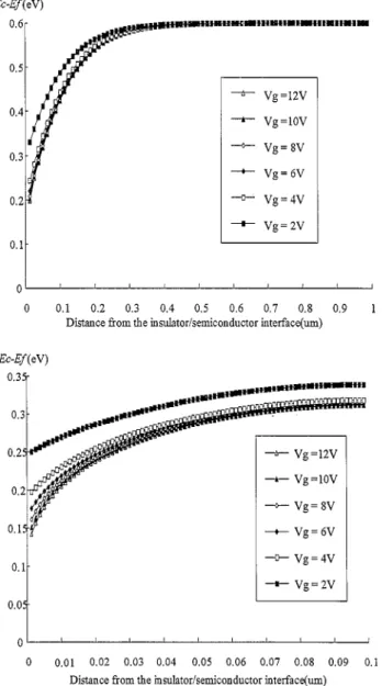
Fig, 2. Potential distributions under various gate bias voltages in the a-Si:H films with thicknesses of (a) 1 pm and (b) 0.1 pm.
widths of 0.07 and 0.05 eV, respectively, as well as a
deep state density of 1017 cmm3 eV-‘. NC and Nv are
both set at lo** cmw3 eV-‘. The band mobility of the
electrons needed for the calculation of Eq. (3) is 10 cm2
V s-l [ll], while the hole mobility is zero, since the ni
source/drain regions will block the conduction of the
holes. The surface DOS and the fixed charges at the
interfaces of the passivation layer/active layer and the
active layer/gate insulator are excluded in this study. By
modifying the distribution of the DOS, the calculated
curve of the field-effect conductance versus the gate
voltage is altered to fit the experimental results. Fur-
thermore, the activation energy of the field-effect con-
ductance was also measured with respect to the gate
voltage. It was in good agreement with the calculated
separation of the Fermi level from the conduction band
edge at the gate insulator/a-Si:H interface [10,12].
Therefore, the validity of this model is confirmed.
3. Results and discussion
The simulated band-bending profiles of the TFTs
with various thicknesses of the semiconductor layer,
biased at the same front interface potential of
EC -Ef
= 0.15 eV, are shown in Fig. 1. It can be seen that
the potential distributions in the active layers with
thicknesses of 1 and 0.5 /lrn are indistinguishable and
approaching the flat band condition near the rear inter-
faces. However, as illustrated in the inset of Fig. 1, for
the TFTs with the a-Si:H films thinner than 0.5 /lrn, the
potential profiles split near the rear interfaces and the
potentials are no longer close to the Fermi level at the
flat band where
EC-
Er= 0.6 eV. With the same gate
bias, the departure of the rear interface potential from
its flat band position increases as the thickness of the
semiconductor film shrinks down.
These phenomena are attributed to the space charges
which must be induced in the semiconductor layer by
the gate bias. In a metal/insulator/semiconductor struc-
ture, the space charge region is formed as the gate
voltage is applied. Assuming the thickness of the semi-
conductor film is infinite, the theoretical width of the
space charge region corresponding to the surface po-
tential is determined by the charges in the semiconduc-
tor and the states at the front interface. For the intrin-
sic a-Si:H film without interface states in this simula-
tion, these space charges consist of the charges trapped
by the states in the energy gap and the free carriers. If
the thickness of the semiconductor is larger than the
principal width of the space charge layer, the potential
distributes as it does in the infinitely thick a-Si:H film,
and the region near the rear interface will not be
affected by the gate voltage, as shown in Fig. 2(a). The
theoretical width of the space charge region, calculated
with the
N(E)of the semiconductor in this study, is
about 0.5 pm. As illustrated in Fig. 2(b), for the
0.1~pm-thick active layer, the Fermi level in the whole
film is forced to move toward the conduction band.
This thin layer cannot afford the required charges ac-
cording to the applied positive gate voltage if the
potential at the rear interface is to stay at its flat band
position. Moreover, for an even thinner a-Si:H film, the
Fermi level will be closer to the conduction band,
because almost the same amount of charges, corre-
sponding to the positive gate voltage, must be gener-
ated in less volume. This is an important feature of
thin-film transistors. In the following context, ‘thin’ film
and ‘thick’ film are used to describe the thicknesses of
the films that are less and greater than the principal
width of the space charge region, respectively.
In thick silicon films, the potential at the rear inter-
face is never affected by the gate bias in the range of the
applied voltages, and the potential profile shifts rigidly
along the distance from the insulator/semiconductor
interface as the potential at the front interface varies, as
Y. Tai et al. / Materials Chemistry and Physics 44 (1996) 182-185 185
shown in Fig. l(a). Therefore, the variation of the conductance of the active layer can be attributed wholly to the change in the potential profile near the front interface. This is the basis of a commonly used tech- nique to extract the DOS of the semiconductor from the field-effect conductance of thin-film transistors. However, the results of this study reveal that the as- sumption of the zero-potential rear interface is im- proper for thin semiconductor films. Therefore, the rigidly shifting behavior of the band bending is not observed in Fig. 2(b), for which the a-Si:H film is thinner than 0.5 pm. In Refs. [2-g], this analysis was applied to TFTs with thick semiconductor films. Thus, the increment of the field-effect conductance can be exclusively correlated to the states near the front inter- face at that particular energy, and the DOS can be extracted. However, for TFTs with thin semiconductor films, the change in the field-effect conductance results from the difference in the band-bending profiles, which cannot be ascribed to a sole energy. Consequently, using the methods presented in Refs. [2-91 to analyze the DOS might lead to incorrect conclusions. The accu- rate DOS in the thin active layer can be obtained by fitting the calculated field-effect conductance with a guessed possible DOS to the experimentally measured data via the proposed procedure.
The thickness effects of the semiconductor films dis- cussed above can also happen in polycrystalline silicon and silicon-on-insulator (SOI) TFTs if the doping con- centration and the DOS of the semiconductor are very low or the active layer is very thin.
4. Conclusions
The band-bending profiles of semiconductor films with different thicknesses in TFTs are calculated. It is found that there is a theoretical width of the space charge region for the metal/insulator/a-Si:H structure.
If the thicknesses of the a-Si:H films are larger than this width, the potential distributes as it would in a film that is infinitely thick. On the other hand, if the semiconduc- tor films are thinner than this width, the potential profiles are greatly affected by the gate bias. The effects of the amorphous-silicon film thickness must be consid- ered in the analysis of the field-effect conductance of TFTs, especially when the active layer is very thin.
Acknowledgements
This research was supported in part by the Republic of China National Science Council (ROC NSC) under Contract No. NSC-79-0425-E009-013. Technical sup- port from the Unipac Optoelectronics Corporation and the National Nano Device Laboratory of ROC NSC is also acknowledged. References [ll PI 131 [41 [51 161 t71 PI [91 [lOI [Ill t121
I. Magarino, Appl. Phys. A, 41 (1986) 297.
N.B. Goodman, H. Fritzsche and H. Ozaki, J. Non-Cryst. Solids, 35/36 (1980) 599.
M.J. Powell, Pkifos Mug. B, 43 (1981) 93.
R.L. Weisfield and D.A. Anderson, PhiLos. Mug. B, 44 (1981) 83. T. Suzuki, Y. Osaks and M. Hirose, Jpn. J. Appl. Phyys., Z(1982)
L195.
M. Shur and M. Hack, J. Appl. Phys., 55 (1984) 3831. R.E.T. Schropp, J. Snijder and J.F. Verwey, J. Appl. Phys., 60
(1986) 643.
G. Fortunato and P. Migliorato, Appl. Phys. Letf., 49 (1986) 1025.
R. Saleh, N. Nickel, W. Fuhs and H. Mell, Muter. Res. Sot. symp. Proc., 219 1991, pp. 339-344.
SC. Deane, F.J. Clough, WI. Milne and M.J. Powell, J. Appl. Phys., 73 (1993) 2895.
R.A. Smith, Hydrogenated Amorphous Silicon, Cambridge Uni- versity Press, New York, 1991, p. 237.
J.G. Shaw and M. Hack, IEEE IEDM, San Francisco, CA, 1992, pp. 915-91s.