IEEE MICROWAVE AND WIRELESS COMPONENTS LETTERS, VOL. 15, NO. 10, OCTOBER 2005 649
A Scalable Noise De-Embedding Technique for
On-Wafer Microwave Device Characterization
Ming-Hsiang Cho, Guo-Wei Huang, Member, IEEE, Yueh-Hua Wang, and Lin-Kun Wu, Member, IEEE
Abstract—In this letter, we present a scalable and efficient noise de-embedding procedure, which is based on transmission-line theory and cascade configurations, for on-wafer microwave mea-surements of silicon MOSFETs. The proposed de-embedding procedure utilizes one open and one thru dummy structures to eliminate the parasitic effects from the probe pads and the input/output interconnects of a device-under-test (DUT), re-spectively. This method can generate the scalable distributed interconnect parameters to efficiently and precisely remove the redundant parasitics of the DUTs with various device sizes and arbitrary interconnect dimensions.
Index Terms—Calibration, de-embedding, MOSFET, noise, -parameters.
I. INTRODUCTION
W
ITH the downscaling device channel length as well as the increasing operation frequency, on-wafer mea-surement and device modeling work on silicon MOSFETs have become more and more significant for RF/microwave circuit design. To extract the intrinsic device performance from measurements, the unnecessary parasitics of the probe pads and input/output interconnects must be exactly removed from the measured data. In previous literature [1]–[3], several parasitic de-embedding methods based on physical equiv-alent-circuit models have been developed and extensively utilized over the past decade. These physics-based methods treat the device-under-test (DUT) as an intrinsic device con-nected to the external parasitics, which come from the probe pads and interconnects, in parallel-series configurations. As the operation frequency becomes higher and/or the interconnect length becomes longer, nevertheless, these equivalent-circuit assumptions may be inappropriate. Recently, a cascade-based de-embedding scheme [4] has been presented, which models the probe pads, interconnects, and the intrinsic device in cas-cade configurations and does not require any equivalent-circuit representation. On the other hand, for the characterization of devices in various sizes, the conventional de-embedding methods mentioned above may occupy considerable chip area for their corresponding dummy structures. Although the ground-shielded measuring technique has been introduced to offer the fixture scalability and mitigate the chip-area con-sumption [5], the scalability of the interconnect parametersManuscript received March 2, 2005; revised May 25, 2005. The review of this letter was arranged by Associate Editor F. Ellinger.
M. H. Cho and G.-W. Huang are with National Nano Device Laboratories, Hsinchu 300, Taiwan, R.O.C. (e-mail: mhcho@mail.ndl.org.tw).
Y.-H. Wang and L.-K. Wu are with the Department of Communication Engi-neering, National Chiao Tung University, Hsinchu 300, Taiwan, R.O.C.
Digital Object Identifier 10.1109/LMWC.2005.856685
Fig. 1. Proposed de-embedding method. (a) DUT and its corresponding dummy structures. (b) Schematic diagram.
for parasitic de-embedding has not been comprehensively studied yet. In our previous work [6], a scalable -parameter de-embedding method based on transmission-line theory and cascade-configuration concept [4] for microwave on-wafer characterization has been presented, and the de-embedding procedure has been verified using thru dummy devices. In this study, we further take the noise parameters into account in the de-embedding procedure and also validate the applicability of the proposed method with measurements on silicon MOSFETs. We find that this scalable de-embedding method is indeed suitable for on-wafer -parameter and noise measurements, especially the on-wafer automatic characterization [7], of multitype and multisize devices. To substantiate the proposed method, MOSFETs fabricated using a standard 0.25- m five-level CMOS process were characterized from 1 to 18 GHz.
II. THEORY OFNOISEDE-EMBEDDING
The proposed de-embedding method is illustrated in Fig. 1. It should be noted that the shield-based structures are not employed in this work for more general consideration. The on-wafer test structures were implemented on silicon sub-strate for microwave characterization of active devices. Unlike the conventional de-embedding methods, which consume a great deal of chip area for dummy patterns, the proposed new theory requires only two dummy structures for parasitic subtraction. After taking away the probe-pad parasitics with the
650 IEEE MICROWAVE AND WIRELESS COMPONENTS LETTERS, VOL. 15, NO. 10, OCTOBER 2005
open dummy, the per-unit-length transmission-line parameters of the thru dummy can be evaluated [6]. Then, DUTs with various device sizes and interconnect lengths can be individ-ually de-embedded with the application of the interconnect scalability.
Similar to the conventional cascade-based method [4], a thru device can be simply modeled in cascade con-nection. After de-embedding the pad parasitics from and converting the chain matrix to its -parameter matrix , where the superscript “ ” denotes the inverse of the matrix and , , and are, respectively, the chain matrices of the intrinsic interconnects, probe pads, and thru dummy, the interconnect characteristic impedance and propagation constant can be calculated as [8]
(1) and
(2) where is the impedance of the -parameter measurement system, is the interconnect length, and
(3)
For the extraction of and , the “ ” signs in (1) and (2) are used to correct the unreasonable solutions, such as negative attenuation constants [8].
Based on the above results, the chain matrices of the input and output interconnects with arbitrary line lengths can be generated by respectively substituting the interconnect lengths and into the chain matrix of a lossy transmission line as
(4) The proposed -parameter and noise de-embedding proce-dure based on cascade connection is listed as follows.
1) Measure the scattering parameters , , and of the DUT, open, and thru, respectively. 2) Measure the noise parameters , , and
of the DUT and calculate the correlation matrix [9].
3) Convert to its admittance matrix and calculate the chain matrix of the probe pads from
(5) 4) Calculate the intrinsic interconnect parameters using
.
5) Convert to its -parameter matrix and calculate the interconnect characteristic impedance and propagation constant based on (1) and (2). 6) Create the chain matrices and
of the input and output interconnects by, respectively, substituting the interconnect lengths and into (4). 7) Calculate the chain matrices of the input port
and the output port using
and ,
respec-tively.
8) Convert to its chain matrix and calculate the chain matrix of the intrinsic
device using .
9) Convert to , where is the intrinsic scat-tering matrix of the DUT.
10) Convert and to their impedance matrices and , respectively.
11) Calculate the noise correlation matrices
and from and
, respectively, where is the Boltzmann’s constant and is the absolute temper-ature.
12) Convert and to their chain
ma-trices and using
and
, respectively, where the superscript “ ” denotes the Hermitian conjugate of the matrix, and the transformation matrix and are
(6) and
(7) 13) Calculate the intrinsic correlation matrix
[9].
14) Calculate the intrinsic noise parameters , , and from the noise correlation matrix using
(8) (9) and
(10)
III. RESULTS ANDDISCUSSION
The on-wafer -parameter and noise measurements were performed with ATN NP5B Noise Parameter Measurement System. To validate the proposed scalable de-embedding pro-cedure for active devices, three n-MOSFETs with the same device dimensions and various interconnect lengths between
CHO et al.: SCALABLE NOISE DE-EMBEDDING TECHNIQUE 651
Fig. 2. Noise parameters versus frequency characteristics (a)NF , (b)R , (c) j0 j, and (d) 0 of three different n-MOSFETs—LS, SL, and SS obtained from measurement results (lines), conventional de-embedding method (open symbols), and proposed de-embedding method (solid symbols). The DUTs are biased atV = 1.5 V and V = 1.15 V (I = 13.3 mA).
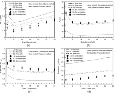
Fig. 3. Noise parameters versus drain current characteristics (a) NF , (b)R , (c) j0 j, and (d) 0 of three different n-MOSFETs obtained from measurement results (lines), conventional method (open symbols), and proposed method (solid symbols) at 18 GHz. The DUTs are biased atV = 1.5 V andI = 1–30 mA.
the probe pads and DUT—LS ( 200 m, 20 m), SL ( 20 m, 200 m), and SS ( 20 m, 20 m), and their corresponding dummy structures were designed and fabricated. The channel length and width of the n-MOSFET are 0.24 and 110 m (10 m 11), respec-tively. The interconnect width and the dimensions of probe pads are 10 and 70 m 70 m, respectively. Fig. 2 shows the measured and de-embedded noise parameters—minimum noise figure , equivalent noise resistance , and
optimized input reflection coefficient versus frequency characteristics of the three MOSFETs biased at 1.5 V and 1.15 V. These results indicate that the intrinsic noise parameters obtained from the conventional cascade-based method [4] and proposed method are in good agreement over the entire frequency range. Fig. 3 exhibits the measured and de-embedded noise parameters versus drain current character-istics of the three MOSFETs at 18 GHz. The interconnects at input port of LS are longer than those of SL and SS and thus have more impact on the measured noise parameters. However, after finishing the noise de-embedding, the intrinsic noise parameters of the three MOSFETs obtained from the conven-tional cascade-based method and proposed scalable method are approximately the same. Based on the above findings, we can use this proposed de-embedding method instead of the conventional one to efficiently calculate the intrinsic noise parameters of the MOSFETs.
IV. CONCLUSION
In this study, a general noise de-embedding method suitable for on-wafer device characterization has been presented and verified with various devices. This method requires only one open and one thru dummy structures to generate the scalable and repeatable interconnect parameters for parasitic subtraction. Therefore, the consumption of chip area for dummy structures can be minimized. Compared with the conventional cascade-based method, the proposed one can eliminate the unwanted par-asitics of the DUTs more efficiently.
REFERENCES
[1] M. C. A. M. Koolen, J. A. M. Geelen, and M. P. J. G. Versleijen, “An improved de-embedding technique for on-wafer high-frequency charac-terization,” in Proc. IEEE Bipolar Circuits Technol. Meeting, 1991, pp. 188–191.
[2] H. Cho and D. E. Burk, “A three-step method for the de-embedding of high-frequencyS-parameter measurements,” IEEE Trans. Electron
Devices, vol. 38, no. 6, pp. 1371–1371, Jun. 1991.
[3] T. E. Kolding, “A four-step method for de-embedding gigahertz on-wafer CMOS measurements,” IEEE Trans. Electron Devices, vol. 47, no. 4, pp. 734–740, Apr. 2000.
[4] C. H. Chen and M. J. Deen, “A general noise and S-parameter deem-bedding procedure for on-wafer high-frequency noise measurements of MOSFETs,” IEEE Trans. Microw. Theory Tech., vol. 49, no. 5, pp. 1004–1004, May 2001.
[5] T. E. Kolding, “Shield-based microwave on-wafer device mea-surements,” IEEE Trans. Microw. Theory Tech., vol. 49, no. 6, pp. 1039–1039, Jun. 2001.
[6] M. H. Cho, G. W. Huang, K. M. Chen, and A. S. Peng, “A novel cascade-based de-embedding method for on-wafer microwave characterization and automatic measurement,” in IEEE MTT-S Int. Dig., Jun. 2004, pp. 1237–1240.
[7] G. W. Huang, D. Y. Chiu, K. M. Chen, Y. M. Deng, and S. C. Wang, “An automatic program suitable for on-wafer characterization, and statistic analysis of microwave devices,” in 61st ARFTG Conf. Dig., Jun. 2003, pp. 157–161.
[8] W. R. Eisenstadt and Y. Eo, “S-parameter-based IC interconnect trans-mission line characterization,” IEEE Trans. Compon., Hybrids,
Manu-fact. Technol., vol. 15, no. 5, pp. 483–483, Aug. 1992.
[9] H. Hillbrand and P. H. Russer, “An efficient method for computer-aided noise analysis of linear amplifier networks,” IEEE Trans. Circuits Syst., vol. CAS-23, no. 4, pp. 235–235, Apr. 1976.