BIST for Crosstalk Faults
DEEP-SUBMICRON TECHNOLOGY’Sadvanced high-density and high-speed VLSI has reduced distances between wires and devices. Perhaps because of manu-facturing defects, parasitic capacitors become important sources of internal circuit noise. In 0.18-µm technology, for example, two parallel lines that are 240 µm long with a spacing of 0.23 µm will produce a 25-fF parasitic capac-itance in the normal fabrication condition.1A manufac-turing defect, such as narrower spacing between two conduction lines, will make the parasitic capacitances even larger. Noise induced by these parasitic elements interferes with normal VLSI operation by generating unex-pected pulses, speeding up or slowing down the transi-tion speed on interconnecting (victim) lines when the nearby aggressor line changes state.2-4If unexpected puls-es appear, and flip-flops catch thpuls-ese pulspuls-es during their sampling time, the system will fall into erroneous states. If the slowed-down transitions exceed the flip-flops’ clock period, erroneous states also result.
Many researchers have focused on analysis, testing, and reduction of crosstalk faults.2-10Chen et al. simply used Kirchoff’s voltage law to analyze crosstalk noise with a three-step approach.2Lee et al. analyzed crosstalk in both frequency and time domains to gain insight into effects that cause errors.3Sabet and Ilponse considered crosstalk on clock or reset lines and contrived a fault simulator to estimate the fault effect and the detectability of crosstalk faults.4Others used proposed algorithms to study circuit
timing characteristics.5-7Bai et al. proposed an at-speed test technique to detect circuit interconnects’ crosstalk faults by generat-ing a six-vector test sequence,8and Lai et al. proposed a software-based self-test methodology to detect crosstalk faults on interconnects.9Several researchers used a timing analy-sis technique to help generate test patterns for crosstalk faults in the desired time window.5,7,8,10
Testing for crosstalk faults is difficult because they are pattern dependent and highly unpredictable. Generating test patterns to deterministically detect these faults requires a timing analysis program of high preci-sion, and this takes much computation time. Previously, we proposed a test scheme based on an oscillation square wave signal.11If a crosstalk fault between two lines exists, applying the square wave test signal on the aggressor line induces glitches on the victim line that can be detected. This scheme eliminates the need to consider the fault timing issue because any glitches induced (usually unexpectedly) by the crosstalk fault are detectable at the victim line’s output.
For the work described in this article, we modified the scheme to test for crosstalk faults of embedded VLSI circuits in the boundary scan environment. The scheme tests for crosstalk faults with a periodic square wave test signal under applied random patterns generated by a linear feedback shift register (LFSR), which is transcon-figured from the embedded circuit’s boundary scan cells. The scheme simplifies test generation and test application while obviating the fault occurrence timing issue. Experimental results show that coverage for the induced-glitch type of crosstalk fault for large bench-mark circuits can easily exceed 90%.12
Using a Periodic Square
Wave Test Signal to
Detect Crosstalk Faults
This BIST scheme simplifies the detection of crosstalk faults in deep-submicron VLSI circuits in the boundary scan environment. Simulation results show that with just a few random patterns, fault coverage for most large benchmark circuits can exceed 90%.
Ming Shae Wu and Chung Len Lee
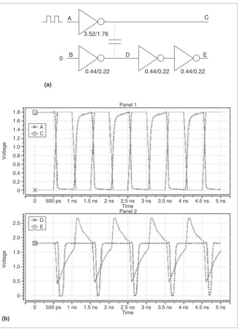
induced glitches caused by crosstalk faults,13but in our scheme we still do a circuit-level simulation for an aggressor line and a victim line to show the induced glitches at the victim’s output. In Figure 1a, a square wave signal con-stitutes the aggressor line’s input, the vic-tim has a static value, and there is a crosstalk fault (the parasitic coupling capacitor between the aggressor and vic-tim lines). The simulated output wave-forms at the victim’s output E appear in Figure 1b, with those waveforms at A, C, D, and E. The figure shows that for this coupling capacitance value, a periodic pulse train appears at E.
Test scheme
Here we describe the basic idea behind the test scheme and illustrate the test scheme architecture.
Basic idea
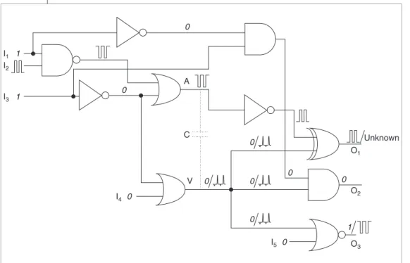
Figure 2 is an example circuit demon-strating the basic idea of how to detect crosstalk faults using the oscillating square wave signal. In the figure, I1, I2, I3, I4, and I5are inputs; O1, O2, and O3are out-puts; line A is the aggressor line; line V is the victim line; and the coupling capaci-tor C represents a coupling fault between lines A and V. When we apply a random test pattern {1, S, 1, 0, 0} to the input (where S stands for an oscillating square wave signal), the output will be {O1, O2, O3= S, 0, 1} if the circuit is fault free. O1= S means that an oscillation square wave
signal appears at O1. However, the exis-tence of coupling fault C between lines
A and V will induce a pulse train at line V. The induced pulse train will propagate to output O3 and be detectable under the applied pattern. Thus, the test has detected coupling fault C.
Test architecture in a boundary scan environment Figure 3 shows the test scheme architecture in a boundary scan environment. The input cells store a
ran-dom pattern generated by an LFSR transformed from boundary scan cells. When testing begins, the tester, under program control, flips the first bit of the input scan cells in polarity and checks all circuit outputs for polar-ity changes. Any output change, say on output Ok,
indi-cates a sensitized path between output Okand the input.
Then the tester applies the oscillating square wave sig-nal S to the input. Pulse trains detected at any output
D B E 0 3.52/1.76 0.44/0.22 0.44/0.22 0.44/0.22 (a) (b) 1.8 1.6 1.4 1.2 1.0 0.8 0.6 0.4 0.2 0 Voltage A C D E 0 500 ps 1 ns 1.5 ns 2 ns 2.5 ns Time 3 ns 3.5 ns 4 ns 4.5 ns 5 ns 2.5 2.0 1.5 1.0 0.5 0 Voltage 0 500 ps 1 ns 1.5 ns 2 ns 2.5 ns Time 3 ns 3.5 ns 4 ns 4.5 ns 5 ns Panel 1 Panel 2
Figure 1. Circuit-level simulation for the induced pulses caused by a crosstalk fault. In the simulated circuit, the parasitic coupling
capacitance is 25 fF, each driver has a 0.18-µm channel length, and the numbers represent the corresponding driver pMOS and nMOS channel width and length ratio of the aggressor and victim lines (a). The input waveform at A produces the simulated waveforms at nodes C, D, and E (b).
other than Okindicate coupling faults between the
sen-sitized paths and victim lines, and this pattern detects the coupling faults. When this test completes, the same procedure repeats on the second input bit, and so on, for all the remaining input bits. Then the LFSR generates another random pattern and stores it in the input cells, and the test procedure runs again. Applying p random patterns for m inputs results in m× p tests. Hence, we can expect very high detection efficiency for the patterns, which the experiment’s results, discussed in a
subse-quent section, verify. For the test described, an oscillator (either built in locally or provided by the SoC in which the cir-cuit under test, or CUT, is embedded) can provide the oscillating square wave signal.
Details of BIST
circuits
Here we describe details of the BIST circuits and the boundary scan cell design.
General description of the circuit
Figure 4 shows the cir-cuit for the BIST architec-ture in the crosstalk fault detection scheme in greater detail. The circuit contains a random pattern generator block (top) and a detector block (bottom) at the input and output of the CUT, which has m inputs and n outputs. The random-pattern generator block contains an m-bit LFSR, where Tclk0 is the clock sig-nal that causes the LFSR to change its state and Sq is the periodic square wave. The shift register’s task is to shift a single logic 1 value from its lowest bit to its highest bit. The shift register outputs connect to an m-bit 2-to-1 multiplex-er, whose outputs could be from the LFSR or the Sq. The detector block contains
■ two D-type flip-flops, which are output boundary cells of the CUT and serve to store the test results of the output;
■ two exclusive-OR gates (XOR1and XOR2);
■ a detection mode latch (DM), which is enabled by the detection mode latch enable to latch the output of XOR1; and
■ an error detector (ED) to detect risky pulses in the output signal.
For one pattern, the circuit has three operational phases: random-test-pattern generation, periodic square wave signal port selection and sensitized-path check-ing, and square wave test. In the first phase, a pulse arrives at Tclk0, and the LFSR changes its state to apply a random pattern to the CUT. The LFSR begins to load
BIST for Crosstalk Faults
0 0 0 0 0 Unknown V O3 O2 O1 I5 0 I4 1 1 I1 I2 I3 C A 0 0 0 0 1
Figure 2. Example circuit demonstrating the test scheme for detecting a crosstalk fault.
Circuit under test S 1 1 0 1
Figure 3. Architecture of the square wave test scheme for crosstalk faults in the boundary scan environment. For one random test pattern applied to the circuit inputs, the tester scans signal S from the inputs’ first bit to the last bit.
logic 1 from its least significant bit (LSB), and the multiplexer selects Sq as its LSB. The second phase identifies the sensi-tized path, and Sq applies 0 and 1 in sequence to the CUT. The first 0’s output result is stored in a D-type positive-edge-triggered flip-flop (DFF1), and the output result of the second 1 remains at the CUT output. XOR1compares these flop, DFF1, and two bits, and its output latches at the DM latch, which the DMLE signal enables at the beginning of this phase. If the DM latch is 1, it means the CUT’s out-put is a sensitized path. In the third phase—square wave test—the tester applies a periodic square wave signal at the rising edge of the test clock to test the circuit. The capture clock (Capclk), the update clock (Updateclk), and the detec-tion clock (Detclk) of the boundary scan cells are synchronized with the test clock. After this phase, the circuit goes back to phase 2 to check another
sensi-tized path because the periodic square wave signal port has been shifted to the second input. Then it returns
again to phase 3, and the process continues.
Figure 5 shows timing diagrams for all the signals of m
m
Detection
mode Error detector
Reset Detection mode latch enable + Circuit under test 10000… n Tclk 1 XOR1 XOR2 Shift register n m bits 2-to-1 multiplexer
D-type flip-flop 1 (DFF1) D-type flip-flop 2 (DFF2) Capture clock Update clock + Detection clock
Figure 4. Circuit detail of the BIST architecture for the crosstalk fault detection scheme.
Tclk Sq Error detector reset signal Capclk0 Updateclk0 Detclk Detection mode latch enable Tclk0 Tclk1 Phase 1 2 3 2
Figure 5. Timing diagrams for the BIST circuit. For one test pattern, the procedure has three phases: test pattern generation (phase 1), periodic square wave signal port selection and sensitized-path checking (phase 2), and square wave test (phase 3). After the third phase, the procedure returns to the second phase, and the process repeats until the periodic square wave signal for the test pattern has been applied to the last input.
the test procedure for testing glitches that affect the cir-cuit operation. The circir-cuit operates at the normal speed, and its output data are shifted into DFF1and DFF2. XOR1compares the outputs of DFF1and DFF2. If the DM latch = 0 (which means the output is not sensi-tized) but the ED detects a 1, the test has detected an unexpected pulse induced by a crosstalk fault.
In Figure 5, Tclk is the test clock, which can be the CUT’s system clock, Capclkoand Updateclkoare the cap-ture register and update register signals, respectively, of the boundary scan cell. The circuit can detect the glitches that propagate to DFF1when DFF1is activated at the rising edge of Capclko. This is the case in which the crosstalk-induced glitches affect the circuit opera-tion in the normal mode. The glitches that arrive before or after the triggering edge of Capclkodo not affect the circuit operation and are ignored.
The scheme aims to detect a combinational block’s
crosstalk-induced glitch faults. Applying it to a sequen-tial circuit requires the sequensequen-tial circuit to be scan designed, and we test only the combinational part. Boundary scan cell design
For the BIST circuit in Figure 4 to support our test scheme, we need to slightly modify the boundary scan cells.
Boundary in cell. The scheme’s boundary
scan-in cells should be able to implement the LFSR function in addition to the cells’ original shifting function. Figure 6 shows the modified 4-bit boundary scan-in cell design with capture and update registers. Each modified boundary scan cell has an added 3-to-1 multiplexer. When transformed into the LFSR mode, the configura-tion is that of a primitive polynomial 1 + x + x4. In the first phase, Tclk0= 1, and the cells are in the LFSR state,
BIST for Crosstalk Faults
Update register coupling_test_mode LFSR/shift_mode Sq boundary_ scan_in scan_in/reload test_mode
Boundary scan-in cell
From pins To circuit + 2-to-1 multiplexer 2-to-1 multiplexer 2-to-1 multiplexer 2-to-1 multiplexer 3-to-1 multiplexer 3-to-1 multiplexer 3-to-1 multiplexer 3-to-1 multiplexer + Capture register Update register Capture register Update register Capture register Update register Capture register
scan_in/reload Output of 2-to-1 multiplexer
0 Output of 3-to-1 multiplexer
1 Previous Capture register output
test_mode, capture register, Output of coupling_test_mode 3-to-1 multiplexer
0xx From pins
10x Update register output
110 Update register output
111 Sq
(a)
(c) (b)
where LFSR/shift_mode and scan_in/reload are set to 1. The capture clock input Capclki, which equals Tclk0at this moment, starts to clock capture registers until their outputs (the random pattern) are finally stored in update registers when the update clock input (Updateclki) signal arrives. In the second phase, the cap-ture registers become shift registers, with the LFSR/shift_mode set to 0. The boundary_scan_in, for one test pattern, is set to 1 at the first phase 2 and is set to 0 at the subsequent phase 2. In addition, coupling_test_mode and test_mode are set to 1. The 3-to-1 multiplexer will select Sq as its input when the cor-responding capture clock’s output is 1. Figure 6 shows the truth tables for the 2-to-1 and 3-to-1 multiplexers.
When scan_in/reload is set to 1 and the LFSR/shift_mode is set to 0, the modified boundary scan-in cells still support the original boundary scan-in function.
Boundary scan-out cell. Figure 7 shows in detail the
design of the boundary scan-out cell for the detector block. In the figure, Detclkis the detector clock. EDR is the error detector reset, which resets the error detector (set to 1 in the first phase of the circuit operation) to 0. In the second phase, DMLE is set to 1, an alternating sequence of 1s and 0s is applied to Sq to check the sen-sitized output, and a pulse arrives at Capclkoto capture the first 1 output to be compared with the second 0 out-put, which appears at line A by XOR1. Finally, the DMLE returns to 0. In the third phase, the Capclko, the update
clock of the boundary scan-out cell (Updateclko), and the Detclkare synchronous with the test clock. The outputs are latched at the capture and update registers at the nor-mal operation speed. XOR1compares two consequent outputs and produces a 1 if these two outputs differ.
Fault coverage estimation through fault
simulation
We performed fault simulation to evaluate the fault coverage of the randomly generated patterns for this test scheme.
Symbol definition and operation
To perform fault simulation, we first introduce and define a set of symbols to represent the various signals and operation rules for each type of gate. Table 1 defines the set of symbols. Figure 8a shows examples of how these symbols operate through an AND gate. For example, C and C* result in PF*, and C and C result in
C. Figure 8b shows the truth tables for AND- and OR-gate
operation. The tables show that these sets of operations are rather conservative. For example, when S operates on S (or S*), an x, indicating an unknown, while for practical cases, an S (or S*) most often results. Fault simulation
The first step for fault simulation is to compute the logic values for the fault-free circuit using the set of vari-ables and operation rules defined in Table 1 and Figure 8. The paths with the S signal are sensitized paths. Then a
Multiplexer
Multiplexer
From last cell scan_out 0x 1 11 10 coupling_ test_mode 0 A B 1 0 test_mode C D E F G Out Capture register Update register Detection mode + + Error detector XOR2
Capclko Updateclko
XOR1
coupling crosstalk fault is injected. If the aggressor line of the crosstalk fault is at one of S (oscillating) paths, the fault site’s victim line is set to C. If this C propagates toward the circuit’s outputs, the propagation is successful, the pattern detects the crosstalk fault, and another fault is injected. This process repeats, eventually injecting all faults; then
the simulator moves on to another pattern. Experimental results
Figure 9 shows the simulation results of the modified boundary scan-out cell of Figure 7 under the timings of Figure 5. In Figure 9, clock signal Tclk, square wave test signal Sq, and control signals DMLE and Detclk(for the DM latch and the ED) appear with the simulated signals at FC (the input of the cell where the induced glitches occur), F (XOR2’s output), and Out (the boundary cell detector’s output). When DMLE is high (that is, the circuit is at the stable logic latch phase, for which Detclkis high), even if there is an induced glitch at FC (at 3.3 ns), the DM latch doesn’t detect the glitch and the boundary cell out-put is low. When DMLE is low (the square wave test phase), if the glitch occurs at the time slot when Detclk is low (at 7 ns), the circuit detects it and the output is high.
To estimate the ran-dom test patterns’ effi-ciency in detecting crosstalk faults, we ran-domly generated patterns to apply to benchmark cir-cuits13into which we ran-domly injected crosstalk faults. We implemented a fault simulator based on our symbols and opera-tion rules to evaluate the fault coverage. For each circuit, we generated two nonoverlapping sets of random crosstalk faults; the number of faults was twice the number of gates. For each fault set, we gen-erated two separate sets of random patterns, each with a different seed for pattern generation.
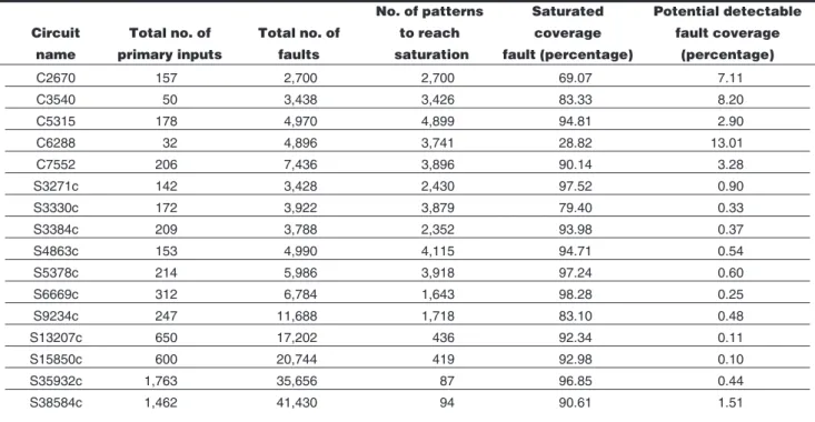
Table 2 (p. 168) shows results for benchmark cir-cuits, where c represents the combinational part of the circuit. Saturated fault coverage depends strongly on the circuit type. For example, for circuits C5315, S13207c, S15850c, and S35932c, which are mainly large
BIST for Crosstalk Faults
Table 1. Symbols for square wave tests. Symbol Representation
0 Static 0
1 Static 1
C* Fault effect signal with positive pulse at logic 0 C Fault effect signal with negative pulse at logic 1 PF* Potential fault effect signal, either 0 or C*
PF Potential fault effect signal, either 1 or C
S* Complement of signal S without considering the timing issue S Periodic square wave signal
x Don’t care C C* C C* C* 0 C & C* = PF* C & C = C C C C C C C (a) (b) AND-gate C PF S x C PF S x x x x C C C C x x x x x x PF PF C PF x x x x x x x x x x S S x x x x x x x x x x x x x x x x OR-gate C PF S x C PF S x PF PF x x x C C PF PF PF x x x PF PF x x x PF PF PF PF PF PF x x x x x x x x x x S S x x x x x x x x x x x x x x x x 0 1 0 0 0 0 0 0 0 0 0 0 0 1 0 0 0 0 0 0 0 0 1 0 1 0 0 1 1 1 1 1 1 1 1 1 1 1 1 1 1 1 1 1 1 1 C* C* C* C* C* S* S* S* S* PF* C* PF* S* C* PF* S* PF* PF* PF* PF* PF* PF* PF* PF* PF*PF* PF* PF* C* C* PF* PF* PF* C* PF* S* C* PF* S*
Figure 8. Examples of AND operation on symbols C and C* (a); operation tables for symbols for AND and OR gates (b).
circuits, it can easily reach 90%; for circuit C6288, which is a multiplier, it reaches only 30%. Also, because of their random selection, some of the faults might be untestable. Fault coverage also depends somewhat on the set of random test patterns, which are generated with different LFSR seeds. However, the difference in fault coverage between two sets of patterns is general-ly small—within 2%. This means that for an arbitrary set
of random patterns, the BIST scheme can detect crosstalk faults quite efficiently, making it very attrac-tive in a practical application.
Table 2 compiles detailed simulation results. The total number of (randomly selected) faults for each cir-cuit is twice the number of gates. The “no. of patterns to reach saturation” column shows the number of random patterns that have been generated by the software LFSR
0 0 2 ns 4 ns 6 ns 8 ns 10 ns 12 ns 1.5 1.0 0.5 0 0 2 ns 4 ns 6 ns 8 ns 10 ns 12 ns Voltage Sq 1.5 1.0 0.5 0 0 2 ns 4 ns 6 ns 8 ns 10 ns 12 ns Voltage Detection mode latch enable 1.5 1.0 0.5 0 0 2 ns 4 ns 6 ns 8 ns 10 ns 12 ns Voltage Detclk 1.5 1.0 0.5 0 0 2 ns 4 ns 6 ns 8 ns 10 ns 12 ns Voltage Cell input 1.5 1.0 0.5 0 0 2 ns 4 ns 6 ns 8 ns 10 ns 12 ns Voltage Output from XOR 1.5 1.0 0.5 0 0 2 ns 4 ns 6 ns Time 8 ns 10 ns 12 ns Voltage Boundary cell detector output
when the fault coverage reached the saturated value, shown in the “saturated fault coverage” column. “Potential detectable fault coverage” is the fault cover-age when one or more PFs or PFs* is detected at the cir-cuit output(s). The table shows that for most circir-cuits, the saturated fault coverage can exceed 90%, with fewer patterns than faults.
THIS ARTICLEdemonstrated a scheme that makes it sim-ple to detect crosstalk faults in deep-submicron VLSI cir-cuits in the boundary scan environment. These faults are difficult to detect by other means. Our BIST scheme is easy to implement and requires minimal modification of the boundary scan cells for the circuit. Simulation results show that with a small number of random patterns for most large circuits, the scheme can detect most crosstalk faults, with fault coverage reaching or exceeding 90%.
References
1.TSMC 0.18um Mixed Signal 1P6M salicide 1.8/3.3v RF SPICE models, Taiwan Semiconductor Manufacturing Corp., 2004; http://www.tsmc.com.tw.
2. W. Chen, S.K. Gupta, and M.A. Breuer, “Analytic Model for Crosstalk Delay and Pulse Analysis Under Non-Ideal Inputs,” Proc. IEEE 1997 Int’l Test Conf. (ITC 97), IEEE
CS Press, 1998, pp. 809-818.
3. K.T. Lee, C. Nordquist, and J.A. Abraham, “Automatic Test Pattern Generation for Crosstalk in Digital Circuits,” Proc. 16th IEEE VLSI Test Symp. (VTS 98), IEEE CS Press, 1998, pp. 34-39.
4. P.B. Sabet and F. Ilponse, “A Model for Crosstalk Noise Evaluation in Deep Submicron Processes,” Proc. 2nd Int’l Symp. Quality Electronic Design (ISQED 01), IEEE CS Press, 2001, pp. 139-144.
5. A. Rubio et al., “An Approach to the Analysis and Detec-tion of Crosstalk Faults in Digital VLSI Circuits,” IEEE Trans. Computer-Aided Design of Integrated Circuits and Systems, vol. 13, no. 3, Mar. 1994, pp. 359-369. 6. N. Itazaki, Y. Idomoto, and K. Kinoshita, “A Fault
Simula-tion Method for Crosstalk Faults in Synchronous Sequen-tial Circuits,” Proc. 26th Int’l Symp. Fault-Tolerant Computing (FTCS 96), IEEE CS Press, 1996, pp. 38-43. 7. Y. Zhao and S. Dey, “Analysis of Interconnect Crosstalk
Defect Coverage of Test Sets,” Proc. IEEE Int’l Test Conf. (ITC 00), IEEE CS Press, 2000, pp. 492-501. 8. X. Bai, S. Dey, and J. Rajski, “Self-Test Methodology for
At-Speed Test of Crosstalk in Chip Interconnects,” Proc. 37th Design Automation Conf. (DAC 00), ACM Press, 2000, pp. 614-624.
9. W.C. Lai, J.R. Huang, and K.T. Cheng, “Embedded-Soft-ware-Based Approach to Testing Crosstalk-Induced Faults at On-Chip Buses,” Proc. 19th IEEE VLSI Test
BIST for Crosstalk Faults
Table 2. Fault simulation results for the proposed BIST scheme.
No. of patterns Saturated Potential detectable Circuit Total no. of Total no. of to reach coverage fault coverage
name primary inputs faults saturation fault (percentage) (percentage)
C2670 157 2,700 2,700 69.07 7.11 C3540 50 3,438 3,426 83.33 8.20 C5315 178 4,970 4,899 94.81 2.90 C6288 32 4,896 3,741 28.82 13.01 C7552 206 7,436 3,896 90.14 3.28 S3271c 142 3,428 2,430 97.52 0.90 S3330c 172 3,922 3,879 79.40 0.33 S3384c 209 3,788 2,352 93.98 0.37 S4863c 153 4,990 4,115 94.71 0.54 S5378c 214 5,986 3,918 97.24 0.60 S6669c 312 6,784 1,643 98.28 0.25 S9234c 247 11,688 1,718 83.10 0.48 S13207c 650 17,202 436 92.34 0.11 S15850c 600 20,744 419 92.98 0.10 S35932c 1,763 35,656 87 96.85 0.44 S38584c 1,462 41,430 94 90.61 1.51
Computational Results,” Proc. 9th Asian Test Symp. (ATS 00), IEEE CS Press, 2000, pp. 305-310. 11. M.S. Wu et al., “A Testing Scheme for Crosstalk Faults
Based on the Oscillation Test Signal,” Proc. 11th Asian Test Symp. (ATS 02), IEEE CS Press, 2002, pp. 170-175. 12. F. Brglez, D. Bryan, and K. Kozminiski, “Combinational
Profiles of Sequential Benchmark Circuits,” Proc. IEEE Int’l Symp. Circuits and Systems (ISCAS 89), IEEE Press, 1989, pp. 1929-1934.
13. M. Cuviello et al., “Fault Modeling and Simulation for Crosstalk in System-on-Chip Interconnects,” Proc. Int’l Conf. Computer-Aided Design (ICCAD 99), IEEE CS Press, 1999, pp. 297-303.
Ming Shae Wu is a PhD student in the Department of Electronics Engi-neering at National Chiao Tung Univer-sity, Taiwan. His main research interest is deep-submicron VLSI testing. Wu
Chung Len Lee is a faculty member in the Department of Electronics Engi-neering at National Chiao Tung Univer-sity, Taiwan. His research interests include IC design, CAD, and testing. Lee has a BS from National Taiwan University and an MS and PhD from Carnegie Mellon University, all in electrical engineering. He is a senior member of IEEE Computer Society.
Direct questions and comments about this article to Chung Len Lee, Department of Electronics Engineering, National Chiao Tung University, Hsin Chu, Taiwan, cllee@mail.nctu.edu.tw.
For further information on this or any other computing topic, visit our Digital Library at http://www.computer.org/ publications/dlib.
IEEE Design & Test Call for Papers
IEEE Design & Test, a bimonthly publication of the IEEE Computer Society and the IEEE Circuits and Systems Society, seeks original manuscripts for publication. D&T publishes articles on current and near-future practice in the design and test of electronic-products hardware and supportive software. Tutorials, how-to articles, and real-world case studies are also welcome. Readers include users, developers, and researchers concerned with the design and test of chips, assemblies, and integrated systems. Topics of interest include
To submit a manuscript to D&T, access Manuscript Central, http://cs-ieee.manuscriptcentral.com. Acceptable file formats include MS Word, PDF, ASCII or plain text, and PostScript. Manuscripts should not exceed 5,000 words (with each average-size figure counting as 150 words toward this limit), including references and biographies; this amounts to about 4,200 words of text and five figures. Manuscripts must be doubled-spaced, on A4 or 8.5-by-11 inch pages, and type size must be at least 11 points. Please include all figures and tables, as well as a cover page with author contact information (name, postal address, phone, fax, and e-mail address) and a 150-word abstract. Submitted manuscripts must not have been previously published or currently submitted for publication elsewhere, and all manuscripts must be cleared for publication.
To ensure that articles maintain technical accuracy and reflect current practice, D&T places each manuscript in a peer-review process. At least three reviewers, each with expertise on the given topic, will review your manuscript. Reviewers may recommend modifications or suggest additional areas for discussion. Accepted articles will be edited for structure, style, clarity, and readability. Please read our author guidelines (including important style information) at http://www.computer.org/dt/author.htm.
Submit your manuscript to IEEE Design & Test today!
D&T will strive to reach decisions on all manuscripts within six months of submission. ■ Analog and RF design,
■ Board and system test, ■ Circuit testing,
■ Deep-submicron technology, ■ Design verification and validation, ■ Electronic design automation, ■ Embedded systems, ■ Fault diagnosis,
■ Hardware/software codesign,
■ IC design and test, ■ Logic design and test, ■ Microprocessor chips, ■ Power consumption, ■ Reconfigurable systems, ■ Systems on chips (SoCs), ■ VLSI; and