© 2008 WILEY-VCH Verlag GmbH & Co. KGaA, Weinheim
p s s
current topics in solid state physics
c
status
solidi
www.pss-c.com
physica
phys. stat. sol. (c) 5, No. 9, 3014 – 3016 (2008) / DOI 10.1002/pssc.200779254
Structural and optical properties
of InN/GaN nanodots grown
by metalorganic chemical vapor deposition
Wen-Hao Chang*, Lin Lee, Ching-Yu Chen, Wen-Che Tsai, Hsuan Lin, Wu-Ching Chou, Ming-Chih Lee, and Wei-Kuo Chen**
Department of Electrophysics, National Chiao Tung University, Hsinchu 300, Taiwan Received 5 October 2007, revised 3 January 2008, accepted 9 January 2008
Published online 2 June 2008
PACS 78.55.Cr, 78.67.Hc, 81.07.Ta, 81.15.Gh
** Corresponding author: e-mail [email protected], Phone: +886-3-5712121ext56111, Fax: +886-3-5715230 ** e-mail [email protected], Phone: +886-3-5712121ext56125
© 2008 WILEY-VCH Verlag GmbH & Co. KGaA, Weinheim
1 Introduction In the past few years, InN thin films with remarkably improved crystalline quality has been re-alized by techniques of molecular beam epitaxy (MBE) [1] and metalorganic chemical vapor deposition (MOCVD) [2]. It has been shown that the energy gap of InN is around 0.69 eV [3, 4], rather than the previously accepted value of ~1.9 eV. Besides the progress in thin film growth, InN nanostructures, such as nanorods [5] and nanodots [6, 7], have also attracted much attention during the last few years. The nucleation process and structural properties of InN nanodots on various substrates have recently been investi-gated [8, 9]. However, only a few reports have been ad-dressed on their photoluminescence (PL) properties.
The difficulty in growing high-optical-quality InN arises not only from the large lattice mismatch between InN and substrates, but also from the low decomposition temperature of InN, which is expected to occur at 520-550°C, leading to a rapid escape of N atoms from the growing surface. If the active nitrogen is insufficient to compensate this decomposi-tion, surface accumulation of metallic In will occur. In MBE growth of InN, this problem may be partially addressed by utilizing low growth temperatures, which is usually below 550°C. However, the situation for MOCVD growth may be
very different, because the thermal cracking of NH3 sources is very inefficient at temperatures below 550°C. In this as-pect, a higher growth temperature is essential in MOCVD growth of InN in order to provide more active nitrogen, but the growth temperature is still limited to around 700°C, due to the desorption of metallic In.
Our previous works have demonstrated that InN nanodots with good optical quality can also be prepared by the flow-rate modulation epitaxy (FME), which is a modi-fied growth technique of MOCVD, wherein the In and N source precursors were supplied alternately [6, 7]. In this study, we focus on the effect of growth temperature on the formation and PL properties of the InN/GaN dots grown by FME and by the conventional MOCVD method (i.e., a continuous growth mode). We found that InN nanodots can be grown at a temperature higher than 700 °C while main-tain their optical quality. The interplay among the NH3 craking efficiency, surface migration of adatoms, decom-position of InN and In desorption in different precursor in-jection schemes are discussed.
2 Experimental Samples were grown on sapphire (0001) substrates in a MOCVD system using trimethylgal-InN nanodots grown on GaN by metalorganic chemical vapor
deposition (MOCVD) using conventional growth mode as well as flow-rate modulation epitaxy (FME) at various growth temperatures (550-730 °C) were investigated. We found that different precursor injection schemes together with the effect of growth temperatures greatly influenced the sur-face morphology of InN dots and their photoluminescence
(PL) properties. The best growth efficiency of InN was achieved by FME at around 650 °C. The residual carrier con-centration and PL efficiency was also be improved when a high growth temperature was used. Our results indicated that InN nanodots can be grown at a temperature even higher than 700 °C while maintain their optical quality.
phys. stat. sol. (c) 5, No. 9 (2008) 3015
www.pss-c.com © 2008 WILEY-VCH Verlag GmbH & Co. KGaA, Weinheim
Contributed Article
lium (TMGa), trimethylindium (TMIn) and ammonia (NH3) as source precursors. The growth pressure was held at 200 mbar. After the growth of a 1-µm-thick undoped GaN buffer layer at 1120°C, the substrate temperature was then lowered to 550-730°C to grow InN nanodots. Two sets of samples have been prepared using FME and con-ventional MOCVD methods at different growth tempera-tures (Tg). In FME, the gas flow sequence in one cycle
consists of four steps: a 20-sec TMIn step, a 20-sec NH3 step, and two 10-sec purge steps of N2 carrier gas inter-vened in between. The TMIn and NH3 flow rates were 150 and 18,000 sccm, respectively, corresponding to molar flow rates of 15.3 and 8.04×10⁵ µmol/min. During the TMIn step, a small amount of NH3 (1,000 sccm) was inten-tionally supplied to suppress the re-evaporation of In atom during this step. The FME growth of InN dots were com-pleted by a total of six cycles for all samples. For the cases of conventional MOCVD growth, continuous flows of 150-sccm TMIn and 10,000- sccm NH3 were supplied for 120 s. Noted that the total amount of TMIn was the same in both growth methods.
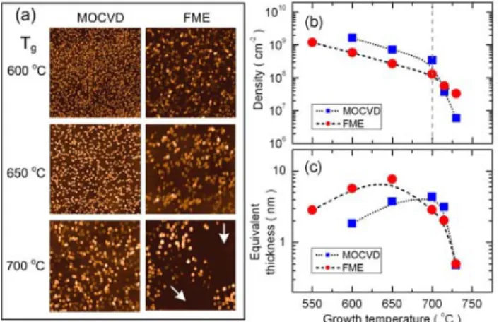
Figure 1 (a) AFM images of InN dots grown at different T by g
FME and by conventional MOCVD. The scanned area for each is 10×10 µm2. (b) The corresponding dot density as a function of
g
T . (c) The deduced equivalent thickness of the deposited InN.
3 Results and discussion Surface morphologies of
InN dots grown by the conventional MOCVD and the FME methods at different Tg are shown in Fig. 1(a). It is clear
that the dot size and density are markedly influenced by the growth temperature. In general, the dot size increases whereas the dot density decreases with the increasing Tg.
The variation of dot density as a function of Tg is depicted
in Fig. 1(b). For the conventional MOCVD growth, two temperature regions divided at about 700°C were displayed. In the low temperature region (T £g 700°C), the dot density
decreases gradually from 7.5 10¥ 9 to 5.0 10¥ 8 cm–2. In the high temperature region (T >g 700°C), the dot density
de-creased rapidly and eventually dropped to zero at
g
T = 750°C. For FME growth, the dot density also de-creases with the increasing Tg, but displaying a less rapid
decreasing trend in the high temperature region.
According to the measured surface morphology, the ef-fective growth rate can be estimated. This can be done by deducing the equivalent thickness of the deposited InN ac-cording the average height, diameter and density of InN dots. Such results are shown in Fig. 1(c). One can see that the highest growth rate was achieved by the FME method at T =g 650°C, corresponding to a growth rate of ~300
nm/hr. The conventional growth generally shows lower growth rate in the low temperature region and exhibits a maximum at T =g 700°C. However, the growth rate for
both growth modes decreases rapidly when T >g 700°C.
As mentioned earlier, the InN growth is controlled by the following three factors: (i) the decomposition of InN, (ii) the thermal cracking of NH3 and (iii) the desorption of metallic In from the growing surface. Because all the three factors are temperature dependent, the different behaviors of surface dot morphologies grown by different methods, and their dependence on Tg, can be understood from the
interplay among these factors together with the different precursor injection schemes. In the low temperature region, the growth of InN is controlled by the amount of active ni-trogen. Therefore, both growth methods show increased growth rate with the increasing Tg, due to the enhanced
thermal cracking of NH3. For T >g 700 °C, the growth of
InN becomes limited by high temperature effects, such as In desorption and parasitic reactions, leading to a rapid de-crease in growth rate for both growth methods. It is note-worthy that the growth rate of FME starts to decrease for
g
T >650°C, which is lower than that for the conventional method. In FME, the growth of InN proceeds only in the TMIn step, during which the background NH3 flow was kept at only 1/10 of that used in continuous growth mode. With the increasing Tg, the small amount of background
NH3 become unable to compensate the thermal decomposi-tion of InN during the TMIn step. As can be seen from the surface morphology shown in Fig. 1(a), FME growth at
g
T >650°C shows some void area (as indicated by arrow), which is very likely to arise from such decomposition of InN and re-evaporation of In. On the contrary, this decom-position of InN is expected to be less significant in the con-ventional MOCVD growth for T £g 700°C, due to the
con-tinuous supply of a high NH3 flow rate. We also noted that the growth rate of the conventional growth mode is slower than that of the FME method for T <g 700°C, most likely
caused by parasitic gas phase reactions between hydrides and In based metalorganic compounds, which may be se-vere due to the simultaneous injections of group-III and group-IV precursors.
The PL spectra for the InN dots grown by FME and MOCVD measured at 10 K are displayed in Figs. 2(a) and 2(b), respectively. No PL signal was observed for samples grown at 550°C. For samples grown at T ≥g 600°C,
near-infrared PL emission bands can be observed in the range of 0.76-0.80 eV. A red shift of the PL peak with the increas-ing Tg can be seen for both FME- and MOCVD-grown
samples. Since the sizes of these InN dots are quite large, (with typically dot height > 20 nm), the energy shift caused
3016 Wen-Hao Chang et al.: Structural and optical properties of InN/GaN nanodots
© 2008 WILEY-VCH Verlag GmbH & Co. KGaA, Weinheim www.pss-c.com
physica
p s s
statussolidi
c
by quantum confinement can be neglected. Therefore, dif-ferences in peak energy between samples are mainly due to variations of the background electron concentration in the InN dots.
Figure 2 The PL spectra of InN dots grown by (a) MOCVD and (b) FME at various T from 600 to 730g ○C. (c) and (d) are the
de-duced carrier concentrations from lineshape model and the inte-grated PL intensity as functions of T , respectively. g
To give a quantitative estimation, we have employed a lineshape model considering “free-to-bond” radiative re-combination to analyze the PL spectra [10]. Since our main interest aims at finding the Fermi energy and hence the rela-tive electron concentration (ne) in different samples, the lineshape model was further simplified by assuming a delta-like function for the energy distribution of photogenerated holes near the valance band edge. In this way, the lineshape of the PL emission band can be approximated by the elec-tron energy distribution in the conduction band [7]. This simplified model reproduces our PL spectra very well, and the deduced ne as a function of Tg is shown in Fig. 2(c). In
general, a lower background carrier concentration in InN can be obtained by using a higher Tg, most likely related to a
more efficient cracking of NH3. We also found that the background carrier concentration of FME grown samples is lower than those grown by conventional method for
g
T <700°C. Since the NH3 flow rate used in conventional growth mode is significantly higher than that used during the TMIn step of FME, we suspect that some donor-type impu-rities are incorporated when a high NH3 flow rate was used.
In Fig. 2(d), the integrated PL intensity as a function of
g
T was displayed. A correlation between the PL intensity and the amount of deposited InN shown in Fig. 1(d) can be seen. If we normalize the PL intensity to the amount of de-posited InN, the PL efficiency as function of Tg can be
ob-tained, which is shown in Fig. 3. One can see that a better PL efficiency can be achieved at higher Tg for both growth
methods. Such an improvement in PL efficiency provides a new approach to the fabrication of high optical quality InN dots for practical applications.
4 Conclusion In summary, the effect of growth temperature on the formation and PL properties of the
Figure 3 The PL efficiency as function of growth temperature. The PL efficiency is obtained by normalizing the measured PL intensity to the amount of deposited InN.
InN/GaN dots grown by FME and by the conventional MOCVD method have been studied. In FME growth of InN, the highest growth rate can be achieved at
g
T =650°C. We found that InN growth is still attainable at
g
T >700°C while maintain its optical quality, but at the expense of lower growth efficiency. Our results also sug-gest that a higher growth temperature is beneficial for both reducing the residual carrier concentration and enhancing PL efficiency.
Acknowledgements This work is supported in part by the project of MOE-ATU and the National Science Council of Tai-wan under grant No. NSC 96-2112-M-009-006, NSC 95-2112-M-009-044-MY3,NSC 2112-M-009-026-MY3, and NSC 96-2112-M-009-014.
References
[1] H. Lu, W. J. Schaff, J. Hwang, H. Wu, G. Koley, and L. F. Eastman, Appl. Phys. Lett. 79, 1489 (2001).
[2] A. Yamamoto, T. Tanaka, K. Koide, and A. Hashimoto, phys. stat. sol. (a) 194, 510 (2002).
[3] V. Yu. Davydov, A. A. Klochikhin, R. P. Seisyan, V. V. Emtsev, S. V. Ivanov, F. Bechstedt, J. Furthmüller, H. Ha-rima, A. V. Mudryi, J. Aderhold, O. Semchinova, and J. Graul, phys. stat. sol. (b) 229, R1 (2002).
[4] J. Wu, W. Walukiewicz, K. M. Yu, J. W. Ager III, E. E. Haller, H. Lu, W. J. Schaff, Y. Saito, and Y. Nanishi, Appl. Phys. Lett. 80, 3967 (2002).
[5] C.-H. Shen, H.-Y. Chen, H.-W. Lin, S. Gwo, A. A. Klochikhin and V. Yu. Davydov, Appl. Phys. Lett. 88, 253104 (2006).
[6] W. C. Ke, C. P. Fu, C. Y. Chen, L. Lee, C. S. Ku, W. C. Chou, W.-H. Chang, M. C. Lee, W. K. Chen, W. J. Lin, and Y. C. Cheng, Appl. Phys. Lett. 88, 191913 (2006).
[7] W. C. Ke, L. Lee, C. Y. Chen, W. C. Tsai, W.-H. Chang, W. C. Chou, M. C. Lee, W. K. Chen, W. J. Lin, and Y. C. Cheng, Appl. Phys. Lett. 89, 263117 (2006).
[8] L. Zhou, T. Xu, D. J. Smith, and T. D. Moustakas, Appl. Phys. Lett. 88, 231906 (2006).
[9] J. G. Lozano, A. M. Sánchez, R. García, D. González, D. Araújo, S. Ruffenach, and O. Briot, Appl. Phys. Lett. 87, 263104 (2005).
[10] B. Arnaudov, T. Paskova, P. P. Paskov, B. Magnusson, E. Valcheva, B. Monemar, H. Lu, W. J. Schaff, H. Amano, and I. Akasaki, Phys. Rev. B 69, 115216 (2004).