IEEE TRANSACTIONS ON DEVICE AND MATERIALS RELIABILITY, VOL. 14, NO. 2, JUNE 2014 781
Local CDM ESD Protection Circuits for Cross-Power Domains in 3D IC Applications
Shih-Hung Chen, Dimitri Linten, Senior Member, IEEE, Mirko Scholz, Yu-Ching Huang, Geert Hellings, Member, IEEE,
Roman Boschke, Ming-Dou Ker, Fellow, IEEE, and Guido Groeseneken, Fellow, IEEE
Abstract—CDM ESD events can be a potential threat to SoC designs or heterogeneous 3D ICs with multiple power domains. Inter-layer (or interface) circuits may need a local CDM ESD clamp that can prevent the unexpected failure under CDM ESD stress. In this letter, two local CDM ESD clamp circuits are proposed. They show better clamping efficiency under 2-ns vfTLP stress.
Index Terms—Electrostatic discharge (ESD), charged device model (CDM), cross-power domains ESD events, 3D stacked ICs, vary-fast trans-mission line pulsing (vfTLP) systems.
I. INTRODUCTION
Due to the increasing requirements for heterogeneous integration in state-of-the-art applications, more advanced and beneficial method-ologies, such as system in a chip (SiC) with 3D vertical integrations, have been proposed in recent years. Such chips, referred to as 3D ICs, are specifically integrated with different physically separated dies connected by miniature vertical metallization structures which can be Through-Silicon-Via (TSV) [1], micro solder bump bonding [2], and so on. Multi-functional blocks are integrated in a SiC and usually possess their individual power/ground supplies for circuit performance requirements and noise coupling prevention. In a heterogeneous 3D in-tegration system, multi-power-domain Electrostatic Discharge (ESD) protection will become a challenge [3], [4], especially for CDM ESD events [5]. Due to the very short rise time and huge amplitude of the CDM ESD peak current, the thin gate oxide of internal transistors can be easily damaged during CDM ESD events. An additional ESD clamp device, such as a gate-grounded NMOS (GGNMOS) [5], is locally added to limit the overvoltage across the internal gate oxide. However, GGNMOS cannot provide an efficient protection of thin gate oxide in nano-scale CMOS IC products, because of its higher trigger voltage under negative CDM ESD stress [6]–[9].
In this work, two CDM ESD protection designs are proposed. With simple trigger circuits, the trigger voltage can be reduced and the turn-on uniformity can be improved. In Sectiturn-ons II and III, the proposed designs are compared with the prior art to show its benefits in 3D IC multi-power-domain applications. Detailed circuit operations of the proposed designs are included in Section III. Section IV shows the verifications of the proposed designs by vfTLP stress. Finally, this abstract closes with the conclusions.
Manuscript received February 27, 2014; revised April 17, 2014; accepted April 21, 2014. Date of publication April 29, 2014; date of current version June 3, 2014.
S.-H. Chen, D. Linten, M. Scholz, and G. Hellings are with the IMEC, 3001 Leuven, Belgium (e-mail: [email protected]; [email protected]; [email protected]; [email protected]).
Y.-C. Huang and M.-D. Ker are with the National Chiao Tung University, Hsinchu 30010, Taiwan (e-mail: [email protected]).
R. Boschke and G. Groeseneken are with IMEC, 3001 Leuven, Belgium, and also with the ESAT Department, Katholieke Universiteit Leuven, 3001 Leuven, Belgium (e-mail: [email protected]).
Color versions of one or more of the figures in this paper are available online at http://ieeexplore.ieee.org.
Digital Object Identifier 10.1109/TDMR.2014.2320538
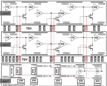
Fig. 1. Schematic illustration of 3D IC applications with the ground current trigger (GCT) technique which needs an external control signal from a different power domain or even from a different layer.
II. ACTIVECDM ESD CLAMP
In order to reduce trigger voltages, some active CDM ESD clamps have been presented [7]–[9]. However, most of them are not optimized for 3D IC applications. The ground current trigger (GCT) technique [7] and the enhanced initial-on PMOS clamp [8], [9] need additional control signals from different power domains or even from different circuit blocks. In 3D IC applications, once the circuit blocks are placed in different dies, the additional control signals will increase the vertical routing effort, for example, more TSVs have to be inserted for the active CDM ESD clamps, as shown in Fig. 1. In addition, the PMOS clamp [8], [9] cannot be used for high voltage to low voltage (HV-to-LV) interfaces and power down mode applications due to an unwanted on-state of the PMOS clamp. Once the potential of VDD2 (the gate node of the PMOS clamp) is lower than the signal path between two different power domains, the PMOS clamp is turned on which induces huge leakage current during normal circuit operation. In order to solve this unwanted leakage path, a special trigger circuit is also proposed in the following session.
III. TWOPROPOSEDDESIGNS
Fig. 2 shows the proposed CDM ESD clamp circuit, Design A, without any external control signals. The main CDM ESD clamp NMOS (Mclamp) is controlled by a one stage inverter (Mp1 and Mn1). The gate terminal of this inverter is connected to the same local VDD2 node.
Under the cross-power domain ESD stress (positive stress from VDD1 to grounded VSS2), the VDD2 is kept floating and the Mp1 can be quickly turned on to trigger the Mclamp. During normal circuit operations, VDD2 is biased at normal VDD potential, the Mp1 and Mclamp are both kept off. However, for HV-to-LV and power down mode applications, Mp1 will be turned on which induces an unwanted Mclamp mis-triggering. Therefore, a special CDM ESD clamp circuit, Design B, is proposed and shown in Fig. 3.
The stacked Mp2 and Mp3 are inserted between the signal path and VDD2. The gate terminal of the inverter is connected to the node, VDD2_E, between Mp2 and Mp3. Under normal circuit operation, 1530-4388 © 2014 IEEE. Personal use is permitted, but republication/redistribution requires IEEE permission.
782 IEEE TRANSACTIONS ON DEVICE AND MATERIALS RELIABILITY, VOL. 14, NO. 2, JUNE 2014
Fig. 2. The proposed Design A which consists of a main ESD clamp NMOS, Mclamp, one stage inverter of Mp1 and Mn1. The inverter is controlled by the VDD2 in the same power domain without any control signal from outside.
Fig. 3. The proposed Design A which consists of a main ESD clamp NMOS, Mclamp, one stage inverter of Mp1 and Mn1. The inverter is controlled by the VDD2 in the same power domain without any control signal from outside.
TABLE I
THEFUNCTIONALSTATE OFEACHDEVICE INDESIGNB WHENVDD2 POTENTIALSAREHIGH, FLOATING,ANDLOWWHICHRESPECTIVELY REFER TONORMALOPERATION, ESD STRESS,ANDPOWERDOWN
MODE. THEARROWSINDICATE THETRANSIENTSWITCH UNDER THECORRESPONDINGSCENARIOS
the VDD2_E node can be charged to the same potential of VDD2 through the on-state Mp3. On the other hand, Mp2 can charge the VDD2_E node also to high in HV-to-LV and power down mode applications. Mp1 and Mclamp can be switched “OFF” preventing thereby an unwanted mis-triggering. In order to ensure the trigger-ing of Mp1 under cross-power-domain ESD stress, the device size of Mp2 must be smaller than that of Mp1. Before the node of VDD_2 is charged up, Mp1 can be kept at “ON” to trigger Mclamp. The functional state of each device in Design B is illustrated in Table I with 3 different scenarios which are the normal operation (VDD2 = “High”), the cross-power-domain ESD stress (VDD2 = “Floating”, and the power down mode (VDD2 = “Low”).
IV. RESULTS ANDDISCUSSION
These two proposed designs are implemented in a 0.13 μm 1.2 V fully silicide CMOS technology with a gate oxide thickness of 2.8 nm. They are verified with 2 ns very fast Transmission Line Pulsing (TLP) with 200 ps rise time. The on-wafer HANWA T5000 TLP/vfTLP tester is used to get insights into the ESD device
char-Fig. 4. The illustrated schematic of the test structures used in this work. ESD stressed on the signal path with the grounded VSS2 to simulate the cross-power domain ESD stress.
Fig. 5. 2-ns vfTLP IV characteristics of traditional GGNMOS and the pro-posed Design A. Design A shows two different discharge modes which are channel conduction and parasitic npn bipolar action of Mclamp.
acteristics in the CDM ESD time domain. All of the test structures are designed in parallel with a gate monitor structure to evaluate the efficiency of the gate oxide protection, as shown in Fig. 4. The gate monitor is NMOS capacitance with the gate length and width of 1 μm. After each vfTLP stress, the 1.2 V DC leakage measurement is executed between signal path and VSS2. The VDD2 is biased at 1.2 V during the leakage measurement.
A. Proposed Design A
Fig. 5 shows the vfTLP IV characteristics of the traditional GGN-MOS and the proposed Design A.
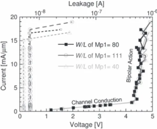
Compared with the traditional GGNMOS, Design A has a better clamping efficiency. Although the failure current level (It2) is slightly lower in Design A, it possesses a lower trigger voltage (V t1) of the parasitic npn bipolar and a lower on resistance (Ron). Design A shows two current conduction modes. At lower vfTLP stress levels, the current is mainly discharged through the channel of Mclamp. Then, as the vfTLP stress levels increases, the current is discharged through the parasitic npn bipolar of Mclamp. At a current level of 14 mA/μm, the clamping voltage of Design A is around 2 V lower than in a traditional GGNMOS. This can be attributed to a more uniform current distribu-tion along the layout width in the proposed Design A due to the gate driven technique. The gate driven capability of Mclamp is dominated by the W/L ratio of Mp1 and Mn1. With same sizes of Mn1, the larger W/L of Mp1 has larger gate driven capability. Fig. 6 shows the vfTLP IV characteristics of Design A with different W/L ratios of Mp1. Besides a small variation of It2, the V t1 and Ron are similar in these three designs. The clamping efficiency is not impacted by the W/L ratio of Mp1 when the W/L ratio of Mp1 is larger than 40.
IEEE TRANSACTIONS ON DEVICE AND MATERIALS RELIABILITY, VOL. 14, NO. 2, JUNE 2014 783
Fig. 6. 2-ns vfTLP IV characteristics of the proposed Design A with different
W/L ratios of Mp1. The W/L ratio does not have strong impact on the trigger
performance.
Fig. 7. 2-ns vfTLP IV characteristics of the proposed Design A and B. Design B shows only one discharge mode which is parasitic npn bipolar action of Mclamp.
B. Proposed Design B
Fig. 7 shows the vfTLP IV characteristics of the proposed Design A and B. Design B does not show two current conduction modes. Mclamp does not provide an efficient channel to discharge the current below 4 V. Then, above 4 V, Mclamp directly switches into the parasitic npn bipolar action. The clamping voltage of Design B is
even lower than the one of Design A. The Ron of these two designs are rather similar, and also the V t1 of the parasitic npn bipolars are both ∼4 V. The similar Ron indicates that the current distribution along the layout width in Design B is as uniform as in Design A. The trigger elements in Design B can well turn-on the parasitic npn bipolar during 2 ns vfTLP stress. However, the holding voltages (V h) of Design A and Design B have a difference of∼0.5 V. The V h of the traditional GGNMOS, Design A and Design B are∼4 V, ∼4.4 V and ∼3.8 V, respectively. The difference implies that the different trigger mechanisms can influence the current distribution between channel conduction and parasitic npn bipolar action during 2 ns vfTLP stress.
V. CONCLUSION
In this work, we propose two local CDM ESD clamps for cross-power-domain interfaces in SoC designs or 3D IC applications. The proposed designs, Design A and B, do not need any external control signals which can cause an additional routing effort in real applica-tions. The proposed Design B can be even used in HV-to-LV interfaces or in power-down mode applications. The experimental results show a better clamping efficiency in Design B. It presents the lowest clamping voltage due to the more suitable current distribution.
REFERENCES
[1] J. Van Olmes et al., “3D stacked IC demonstration using through Silicon via first approach,” in IEDM Tech. Dig., 2008, pp. 1–4.
[2] A. Yu et al., “Study of 15 μm pitch solder microbumps for 3D IC integra-tion,” in Proc. ECTC, 2009, pp. 6–10.
[3] M.-D. Ker, “ESD protection circuit for mixed mode integrated circuits with separated power pins,” U.S. Patent 6 075 686, Jun. 16, 2000.
[4] E. Worley, “Distributed gate ESD network architecture for inter-power domain signals,” in Proc. EOS/ESD Symp., 2004, pp. 1–10.
[5] S.-H. Chen et al., “Active ESD protection circuit design against charged-device-model ESD event in CMOS integrated circuits,” J. Microelectron.
Rel., vol. 47, no. 9–11, pp. 1502–1505, 2007.
[6] N. Kitagawa, H. Ishii, J. Watanabe, and M. Shiochi, “An active ESD protection technique for the power domain boundary in a deep submicron IC,” in Proc. EOS/ESD Symp., 2006, pp. 196–204.
[7] M. Okushima, “ESD protection design for mixed-power domains in 90 nm CMOS with new efficient power clamp and GND current trigger (GCT) technique,” in Proc. EOS/ESD Symp., 2006, pp. 205–213.
[8] S.-H. Chen, M.-D. Ker, and H.-P. Hung, “Active ESD protection design for interface circuits between separated power domains against cross-power-domain ESD stresses,” IEEE Trans. Device Mater. Rel., vol. 8, no. 3, pp. 549–560, Sep. 2008.
[9] C.-Y. Lin and M.-D. Ker, “CDM ESD protection design with initial-on concept in nanoscale CMOS process,” in Proc. IPFA, 2010, pp. 1–4.