國 立 交 通 大 學
電子工程學系 電子研究所碩士班
碩 士 論 文
應用於射頻積體電路之靜電放電防護設計
ESD Protection Design for Radio-Frequency Integrated
Circuits
研 究 生: 蔡翔宇 (Shiang-Yu Tsai)
指導教授: 柯明道教授 (Prof. Ming-Dou Ker)
應用於射頻積體電路之靜電放電防護設計
ESD Protection Design for Radio-Frequency Integrated
Circuits
研 究 生:蔡翔宇
Student: Shiang-Yu Tsai
指導教授:柯明道教授
Advisor: Prof. Ming-Dou Ker
國立交通大學
電子工程學系
電子研究所
碩士論文
A Thesis
Submitted to Department of Electronics Engineering and Institute of Electronics
College of Electrical and Computer Engineering
National Chiao Tung University
in Partial Fulfillment of the Requirements
for the Degree of
Master of Science
in
Electronics Engineering
August 2012
HsinChu, Taiwan, Republic of China
i
應用於射頻積體電路之靜電放電防護設計
學生: 蔡 翔 宇 指導教授: 柯 明 道 教授
國立交通大學
電子工程學系 電子研究所碩士班
摘要
在現今的 IC 設計中,晶片的整合度與成本是相當重要的考量,因此,射頻積體電 路 (radio-frequency integrated circuits, RF ICs) 也逐漸傾向於實現在 CMOS 製程中。在 CMOS 製程中,靜電放電 (electrostatic discharge, ESD) 是一項相當重要的可靠度問題,因此針對使用 CMOS 製程的射頻積體電路之靜電放電防護設計自然也是需求孔 急。由於射頻積體電路對於任何額外的寄生效應都相當敏感,因此能應用在射頻積體電 路之靜電放電防護設計除了要有好的靜電放電耐受度之外,還必須要能將其寄生效應的 影響降至最低。 本篇論文提出了兩項可應用在射頻積體電路之靜電放電防護設計。其中之一可應用 於 60 GHz 的射頻積體電路,透過適當設計的電感 (inductor) 與電容 (capacitor),能夠 在高頻下將寄生效應的影響降低,同時又能兼顧一定的靜電放電防護能力。
ii
透過一個使用齊納二極體 (Zener diode) 來觸發的的矽控整流器 (silicon-controlled rectifier, SCR) 來 做 為 靜 電 防 護 元 件 , 並 搭 配 電 源 端 到 地 端 間 靜 電 放 電 箝 制 電 路
(power-rail ESD clamp circuit) 來完成全晶片防護,同時搭配 2.4 GHz 之射頻功率放大
器電路以作驗證。
根據量測結果,這些設計可以有效的提供射頻積體電路適當的靜電放電防護能力, 同時又不會影響其正常操作。
iii
ESD Protection Design for Radio-Frequency Integrated
Circuits
Student: Shiang-Yu Tsai
Advisor: Prof. Ming-Dou Ker
Department of Electronics Engineering &Institute of Electronics
National Chiao-Tung University
Abstract
For the consideration of high integration and low cost, radio-frequency integrated circuits
(RF ICs) have been fabricated in CMOS processes. Electrostatic discharge (ESD) is one of the
most serious reliability issues of CMOS processes, and it also bothers RF IC designers now.
A successful RF ESD protection design needs well ESD protection ability and small parasitic
effect, since RF ICs are very sensitive to any extra parasitic effect.
In this thesis, two RF ESD protection designs are proposed and verified. One is for RF
circuits operating in 60 GHz. With the help of inductor and capacitor, the parasitic
capacitance of ESD protection device can be effectively decreased and acceptable ESD level
can be required.
The other one is for RF power amplifier (PA). A Zener-diode-triggered silicon-controlled
iv
with the proposed ZTSCR and power-rail ESD clamp circuit are designed as ESD-protected
PAs to verify their ESD level.
According to the experimental results, the ESD protection designs have high ESD
v
Acknowledgment
在碩士班的兩年之中,首先要感謝柯明道老師的細心指導與耐心鼓勵,老師在ESD 方面深厚的專業知識以及殷切的指導讓我在兩年之中學到了許多東西,而在專業領域之 外,老師認真的研究態度與方法也讓我獲益良多。 感謝任職於台灣積體電路的魏佑霖先生、張子恒先生、蔡銘憲先生、傅淑芳小姐、 李孝純小姐在晶片下線實作上的幫忙,讓各個設計都能順利成功驗證。 感謝實驗室的學長姐們在研究生活各方面的不吝幫忙。特別要感謝竹立煒學長,在 模擬、設計、實作、量測等等各方面都給予我極大的幫助,有他的幫助才能讓我順利完 成研究。還要感謝林群佑學長的協助,在研究上的一些大大小小的問題都能幫我解決。 也要感謝實驗室的邱柏硯學長、葉致廷學長、陸亭州學長、蔡惠雯學姐、艾飛學長,還 有去年從實驗室畢業的李易儒學長跟黃筱晴學姐等人的幫助,讓我的研究所生活能更充 實。 還有跟我同屆的戴嘉岑、黃雅君、郭品宏三位研究夥伴,雖然彼此研究領域不盡相 同,但是有問題大家還是會一起討論,一起研究。感謝大家這兩年的陪伴,讓我的碩班 生活不會孤單。 最後當然要感謝無條件支持、照顧和陪伴我的家人,讓我能無後顧之憂的完成學 業。感謝這一路上陪伴我的所有人,願大家都能平安順利,謝謝。 蔡翔宇 101年8月於交大vi
Contents
摘要……….. ... i Abstract…… ... iii Acknowledgment ... v Contents….. ... viTable Captions ... viii
Figure Captions ... ix
Chapter 1 Introduction ... 1
1.1 Motivation ... 1
1.2 Thesis Organization... 3
Chapter 2 Basics of RF and ESD Protection ... 5
2.1 General Considerations of LNA Design ... 5
2.1.1 S-Parameters and Noise Figures ... 5
2.1.2 Stability... 7
2.2 General Considerations of PA Design ... 8
2.2.1 Efficiency and Large Signal Characteristics ... 8
2.2.2 Load-Line Theory and Load-Pull Characterization ... 10
2.2.3 Classes of Conventional Linear PA ... 14
2.3 Conventional ESD Protection Design ... 15
2.3.1 Architecture of Conventional Whole-Chip ESD Protection Design .... 15
2.3.2 Power-Rail ESD Clamp Circuit and I/O ESD Clamp Device ... 16
2.4 Issues of RF ESD Protection Design ... 20
2.4.1 Impacts of ESD Protection Design on RF Performance ... 20
2.4.2 Challenges of RF ESD Protection Design ... 22
2.4.3 Conventional RF ESD protection designs ... 23
Chapter 3 ESD Protection Design for 60 GHz RF Circuits ... 30
3.1 Challenges of ESD Protection Design for 60 GHz RF Circuits ... 30
3.2 Architecture of The Proposed ESD Protection Designs ... 31
3.3 ESD Discharge Paths of the Proposed ESD Protection Designs ... 34
3.4 Simulation Results ... 37
3.5 Experimental Results ... 37
3.5.1 Test Circuits ... 37
3.5.2 Measured RF Performance ... 39
3.5.3 Measured ESD Robustness ... 42
vii
Chapter 4 ESD Protection Design for 2.4 GHz CMOS RF PA ... 45
4.1 Traditional ESD Protection Design for PA ... 45
4.2 Proposed ESD Protection Design for PA... 46
4.3 Experimental Results of ZTSCR ... 52
4.3.1 Test Devices... 52
4.3.2 Experimental Results ... 53
4.4 Circuit Design of 2.4 GHz CMOS RF PA ... 57
4.4.1 Circuit Design ... 57
4.4.2 Post-Simulation Results ... 58
4.5 Experimental Results of 2.4 GHz CMOS PA with ZTSCR ... 62
4.5.1 The Layout Description of Unprotected PA and ESD-protected PA .... 62
4.5.2 ESD Levels Measured with HBM ESD Tester ... 65
4.5.3 Measured RF Performance of the Unprotected PA ... 68
4.5.4 Comparison of RF Performance before ESD Stress ... 71
4.5.5 Comparison of RF Performance after ESD Stress ... 74
4.6 Discussion ... 83
4.7 PA ESD Protection Design Consists of RF Choke Inductor and Power-Rail ESD Clamp Circuit ... 84
Chapter 5 Conclusions and Future Works ... 89
5.1 Conclusions ... 89
5.2 Future Works ... 90
Reference…. ... 91
Vita……….. ... 93
viii
Table Captions
Table 3.1 Device Parameters of Proposed ESD Protection Designs ... 38
Table 3.2 Comparisons of Experimental Results Among ESD Protection Circuits in Silicon.. ... 43
Table 4.1 Junction Dimensions of Each Split of ZTSCR ... 53
Table 4.2 Measurement Results of Each Split of ZTSCR ... 55
Table 4.3 Component values and device dimensions of the 2.4 GHz CMOS PA ... 59
Table 4.4 Summary of the post-simulation results of the 2.4 GHz CMOS PA ... 62
Table 4.5 Measured ESD level of each zapping mode with HBM tester ... 67
Table 4.6 Summary of the measurement results of the 2.4 GHz CMOS PA ... 71
Table 4.7 Summary of RF performance of the unprotected PA and the ESD-protected PA after HBM ESD zapping ... 82
ix
Figure Captions
Fig. 2.1. A two-port network described with S-parameters. ... 6
Fig. 2.2. A cascade multi-stage RF system described with gain and noise factor. ... 7
Fig. 2.3. The plots of power gain versus input power. ... 10
Fig. 2.4. The plots of output power versus input power. ... 10
Fig. 2.5. Architecture of general RF power amplifier. ... 11
Fig. 2.6. (a) A simple current generator and (b) the comparison of its two output matching methods. ... 12
Fig. 2.7. Typical Load-pull system. ... 13
Fig. 2.8. Load-pull contour – delivered power contour. ... 13
Fig. 2.9. Load-pull contours – delivered power contour and PAE contour. ... 14
Fig. 2.10. Comparison among different bias points and there corresponding types of PA. 15 Fig. 2.11. Architecture of whole-chip ESD protection design. ... 16
Fig. 2.12. Typical power-rail ESD clamp circuit. ... 17
Fig. 2.13. Conventional whole-chip ESD protection design. ... 18
Fig. 2.14. ESD-discharge paths under (a) PS-mode and NS-mode, (b) PD-mode and ND-mode, and (c) VDD-to-VSS mode and VSS-to-VDD mode. ... 19
Fig. 2.15. Conventional ESD protection design with double diodes and a power-rail ESD clamp circuit for LNA. ... 20
Fig. 2.16. LNA with parasitic impedance of input pad and ESD protection diodes for calculating the power gain. ... 22
Fig. 2.17. ESD protection design with LC-tanks for RF circuits. ... 24
Fig. 2.18. ESD protection design with series diodes and inductors for RF circuits. ... 25
Fig. 2.19. Input matching co-design of RF circuits with ESD protection devices. ... 26
Fig. 2.20. ESD protection devices with decreasing size for broad-band RF circuits. ... 27
Fig. 2.21. The (a) cross-section view and (b) equivalent circuit of a typical SCR. ... 28
Fig. 2.22. I–V characteristics of SCR device under positive and negative voltage biases. . 29
Fig. 3.1. Proposed ESD protection design A with supplement capacitor and power-rail ESD clamp circuit. ... 33
Fig. 3.2. Proposed ESD protection design B and power-rail ESD clamp circuit. ... 33
Fig. 3.3. ESD discharge path of the proposed design A under PS-mode. ... 34
Fig. 3.4. ESD discharge path of the proposed design A under PD-mode. ... 35
Fig. 3.5. ESD discharge path of the proposed design A under NS-mode. ... 35
Fig. 3.6. ESD discharge path of the proposed design A under ND-mode. ... 36
Fig. 3.7. ESD discharge path of the proposed design A under VDD-to-VSS and VSS-to-VDD mode. ... 36
x
Fig. 3.8. Simulated S21 parameter of the proposed design. ... 37
Fig. 3.9. Layout top view of the test circuit A4. ... 39
Fig. 3.10. Measured S21 parameters of proposed design A within (a) 0~67 GHz and (b) 57~63 GHz. ... 40
Fig. 3.11. Measured S21 parameters of proposed design B within (a) 0~67 GHz and (b) 57~63 GHz. ... 41
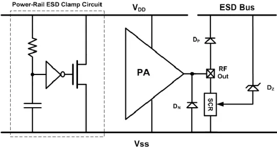
Fig. 4.1. Traditional ESD protection design for PA and its longest ESD discharge path. . 46
Fig. 4.2. The proposed ESD protection design for PA. ... 47
Fig. 4.3. The proposed ESD protection design with a Zener diode as the trigger circuit of the SCR. ... 48
Fig. 4.4. The (a) cross-section view and (b) the equivalent circuit of the ZTSCR. ... 49
Fig. 4.5. ESD discharge path of the ZTSCR under PS-mode. ... 50
Fig. 4.6. ESD discharge path of the ZTSCR under NS-mode. ... 50
Fig. 4.7. ESD discharge path of the ZTSCR under PD-mode. ... 51
Fig. 4.8. ESD discharge path of the ZTSCR under ND-mode. ... 51
Fig. 4.9. ESD discharge path of the ZTSCR under VDD-to-VSS mode and VSS-to-VDD mode. ... 52
Fig. 4.10. Cross-section view of ZTSCR with several junctions which are used to do splits... ... 53
Fig. 4.11. Layout top view of split 1-6 of ZTSCR. ... 54
Fig. 4.12. TLP-measured I-V characteristics of split 1-6. ... 56
Fig. 4.13. Tek370-measured DC I-V characteristics of split 1-6. ... 56
Fig. 4.14. Simple architecture of a two-stage power amplifier. ... 57
Fig. 4.15. The circuit diagram of the 2.4 GHz two-stage CMOS PA. ... 58
Fig. 4.16. Simulated S-parameters of the 2.4 GHz CMOS PA. ... 60
Fig. 4.17. Simulated power gain of the 2.4 GHz CMOS PA. ... 60
Fig. 4.18. Simulated output power of the 2.4 GHz CMOS PA. ... 61
Fig. 4.19. Simulated PAE of the 2.4 GHz CMOS PA. ... 61
Fig. 4.20. Unprotected PA without the output matching network. ... 63
Fig. 4.21. Type I of the ESD-protected PA. ... 64
Fig. 4.22. Type II of the ESD-protected PA. ... 65
Fig. 4.23. Die photo of the unprotected PA. ... 66
Fig. 4.24. Die photo of type I of the ESD-protected PA. ... 66
Fig. 4.25. Die photo of type II of the ESD-protected PA. ... 67
Fig. 4.26. Measured S11 parameter of the unprotected PA... 68
Fig. 4.27. Measured S21 parameter of the unprotected PA. ... 69
Fig. 4.28. Measured power gain of the unprotected PA. ... 69
Fig. 4.29. Measured output power of the unprotected PA. ... 70
xi
Fig. 4.31. Comparison of S11 Parameter of the unprotected PA and the ESD-protected
PA….. ... 72
Fig. 4.32. Comparison of S21 Parameter of the unprotected PA and the ESD-protected PA….. ... 72
Fig. 4.33. Comparison of power gain of the unprotected PA and the ESD-protected PA. .. 73
Fig. 4.34. Comparison of output power of the unprotected PA and the ESD-protected PA.73 Fig. 4.35. Comparison of PAE of the unprotected PA and the ESD-protected PA. ... 74
Fig. 4.36. Power gain of the unprotected PA after HBM ESD zapping... 75
Fig. 4.37. Output power of the unprotected PA after HBM ESD zapping... 75
Fig. 4.38. PAE of the unprotected PA after HBM ESD zapping. ... 76
Fig. 4.39. Output power of type I of the ESD-protected PA after HBM ESD zapping. ... 76
Fig. 4.40. Power gain of type I of the ESD-protected PA after HBM ESD zapping with input power ranging from (a) -20 dBm to 15 dBm and (b) -20 dBm to 0 dBm. . 77
Fig. 4.41. PAE of type I of the ESD-protected PA after HBM ESD zapping with input power ranging from (a) -20 dBm to 15 dBm and (b) 5 dBm to 15 dBm. ... 78
Fig. 4.42. Power gain of type II of the ESD-protected PA after HBM ESD zapping with input power ranging from (a) -20 dBm to 15 dBm and (b) -20 dBm to 0 dBm. . 79
Fig. 4.43. PAE of type II of the ESD-protected PA after HBM ESD zapping with input power ranging from (a) -20 dBm to 15 dBm and (b) -20 dBm to 0 dBm. ... 80
Fig. 4.44. Output power of type II of the ESD-protected PA after HBM ESD zapping. ... 81
Fig. 4.45. EMMI picture of type II of the ESD-protected PA after 4-kV HBM zapping of every mode. The failure location is at the ZTSCR added to E2 pad. ... 81
Fig. 4.46. SEM picture of type II of the ESD-protected PA after 4-kV HBM zapping of every mode. ... 82
Fig. 4.47. ESD protection strategy for PA with the RF choke inductor LESD and a power-rail ESD clamp circuit. ... 84
Fig. 4.48. ESD discharge paths under PS-mode and NS-mode ESD stress. ... 85
Fig. 4.49. ESD discharge paths under PD-mode and ND-mode ESD stress. ... 86
Fig. 4.50. Circuit diagram of the ESD-protected PA circuit. ... 86
Fig. 4.51. Die photo of the ESD-protected PA. ... 87
Fig. 4.52. Measured S21 parameters of the ESD-protected PA before and after HBM ESD stress of 4 kV. ... 87
1
Chapter 1
Introduction
1.1 Motivation
In recent decades, the development of wireless technologies is explosive and rapid. The
requirements of wireless products such as smart phones are overwhelming. For the
consideration of low cost and high integration, the whole radio-frequency integrated circuits
(RF ICs) have been widely fabricated in CMOS processes [1].
The major reliability issue of CMOS ICs is electrostatic discharge (ESD). As IC
technology continuously scales down, ESD issues become more serious and must be carefully
considered. Well-designed ESD protection circuits for all I/O pads in ICs are necessary.
Conventional ESD protection design, which consists of a pair of diodes inserted beside I/O
pads and a power-rail ESD clamp circuit can provide whole-chip ESD protection [2].
Unfortunately, such design would degrade the RF performance of core circuits due to the
undesired parasitic effects introduced by those ESD protection devices [3].
ESD protection devices are mainly applied to the I/O interfaces of ICs. For an RF IC, the
input interface is typically a low-noise amplifier (LNA), and the output interface is typically a
power amplifier (PA). Thus, ESD protection design for CMOS LNA and PA are needed.
While being applied in RF ICs, conventional ESD protection devices with large
dimensions have good ESD robustness, but their large parasitic capacitances cause power loss
from pads to ground. In addition, the parasitic capacitances also change input and output
2
degrading the RF performance of core circuits has become a great challenge.
Since the parasitic capacitances of ESD protection devices are the main obstacle to RF
ESD protection design, some methods have been developed to mitigate the negative impact
caused by the parasitic capacitances. The parasitic capacitances of ESD protection devices can
be cancelled out by using inductors and capacitors [4]-[6]. Some ESD protection designs have
been developed to fundamentally reduce the parasitic capacitances of the ESD protection
devices [3]. ESD protection devices can also be co-designed with RF circuits or combined
with matching networks of RF circuits [7].
However, the rapidly increasing operating frequency of RF ICs makes the parasitic
capacitances of ESD protection devices be more strictly limited. It is harder and harder to
meet the desired ESD robustness with such limitation. As a result, ESD protection designs for
extremely high frequency are necessary. Two new ESD protection circuits with less RF
performance degradation and compact layout area are proposed in this work. Both ESD
protection circuits are designed for 60 GHz RF circuits. Such ESD protection circuits have
been designed and fabricated in a 65-nm CMOS process. The measurement results prove that
both ESD protection designs are suitable for 60 GHz RF circuits with required ESD
robustness and tolerable degradation of RF performance.
Another ESD protection design for CMOS PA is also proposed in this work. For RF ESD
protection designs, silicon-controlled rectifier (SCR) is a useful device. An SCR with proper
triggering mechanism has great ESD robustness and low parasitic capacitances within a small
layout area. Therefore, carefully designed SCR is expected to be suitable for RF ESD
protection [8]. A Zener-diode-triggered SCR (ZTSCR) for PA ESD protection is proposed.
Two 2.4 GHz CMOS PAs which utilize ZTSCR and a power-rail ESD clamp circuit as their
ESD protection design are presented. The ZTSCR and PAs have been designed and fabricated
in a 65-nm CMOS process. The measurement results show that ZTSCR indeed provides
3
Besides, for comprehensive investigation of PA ESD protection methods, an
ESD-protected PA with ESD protection strategy consists of an RF choke inductor and a
power-rail ESD clamp circuit has also been designed and verified in a 65-nm CMOS process.
Such ESD protection strategy is used for PA with on-chip RF choke inductor at the output
stage. According to the measurement results, the proposed ESD protection strategy also
provides desired ESD robustness without degrading PA RF performance.
1.2 Thesis Organization
Chapter 2 introduces the basic principles and the crucial considerations of RF ESD
protection design as well as basics of RF LNA and RF PA. The issues of RF ESD protection
design are investigated. Some practical RF ESD protection designs are exhibited.
Chapter 3 exhibits ESD protection designs for 60 GHz RF circuits. Two ESD protection
designs with inductors, capacitors, and diodes are proposed. The architecture, corresponding
design equations, and simulation results are presented. The measurement results of the RF
performances and the ESD levels of both ESD protection designs, which are fabricated in a
65-nm CMOS process, are summarized. According to the experimental results, the two
proposed ESD protection designs exhibit required ESD levels without serious RF
performance degradation, and therefore is suitable for 60 GHz RF circuits.
Chapter 4 exhibits an ESD protection design for 2.4-GHz RF PA. A
Zener-diode-triggered SCR, which is appropriate for PA ESD protection, is proposed. The
architecture of the ESD protection design is presented in detail. In addition, a 2.4 GHz CMOS
PA used to verify the ESD level of the proposed ZTSCR is also designed. Both unprotected
PA and ESD-protected PA are fabricated in a 65-nm CMOS process. The experimental results
4
summarized and compared. According to the results, the proposed ZTSCR indeed has enough
ESD protection ability without degrading the RF performances of the 2.4 GHz CMOS PA.
Besides, a useful ESD protection design for PA with on-chip RF choke inductor at the output
stage is also presented and verified in a 65-nm CMOS process.
5
Chapter 2
Basics of RF and ESD Protection
2.1 General Considerations of LNA Design
2.1.1 S-Parameters and Noise Figures
To deal with a high-frequency network, conventional method of measuring voltage and
current is no longer suitable. Direct measurement under high-frequency conditions usually
involves the magnitude and phase of a traveling wave, so the concepts of equivalent voltage,
equivalent current, and the related impedance and admittance become abstract. Scattering
parameters (S-parameters) with the concepts of incident, reflected, and transmitted waves are
more suitable and widely used to describe the characteristics and behaviors of high-frequency
networks [9].
Fig. 2.1 shows a two-port network characterized by S-parameters. The S-parameters are
defined in 1 11 12 1 21 22 2 2 b S S a S S b a (2.1)
which can also be represented as
1 11 1 12 2 2 21 1 22 2 b S a S a b S a S a (2.2)
where a1 and a2 represent the incident waves of each port; b1 and b2 represent the reflected
waves of each port, respectively. Each term in the S-parameters matrix is defined in (2.3).
2 1 11 1 a 0 b S a
6 1 1 12 2 a 0 b S a 2 2 21 1 a 0 b S a 1 2 22 2 a 0 b S a (2.3)
S11 is the reflection coefficient seen at port 1 when port 2 is terminated with a load of 50 ;
S22 is the reflection coefficient seen at port 2 when port 1 is terminated with a load of 50 .
S21 is the forward gain from port 1 to port 2; S12 is the reverse gain from port 2 to port 1.
In high-frequency measurement, S11 describes input matching condition, and S22
describes output matching condition. S21 describes the forward gain from port 1 to port 2, and
S12 describes the reverse isolation condition.
Fig. 2.1. A two-port network described with S-parameters.
For receivers, noise is another important concern. Noise factor is a figure of merit to
describe a noisy system [10]. Noise factor is defined as
i o SNR F SNR (2.4)
where SNRi represents the signal-to-noise ratio measured at input, and SNRo represents the
signal-to-noise ratio measured at output. It is a measure of SNR degradation when signal
passes through the described system. A commonly used figure of merit named noise figure
7
10log ( )
NF F dB
(2.5)
The physical meaning can be realized as
Total output noise power NF
Output noise power due to source only
(2.6)
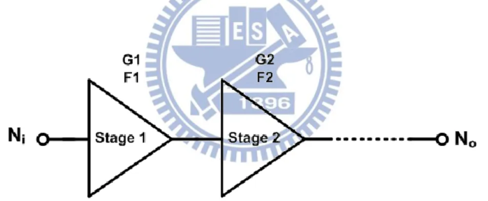
Form (2.6), if the described system adds no noise of its own, NF would be zero.
Considering a cascade multi-stage system shown in Fig. 2.2, each stage has gain (G) and
noise factor (F). The noise factor can be characterized by Friis formula
3 2 1 1 1 2 1 1 1 ( 1) ... sys F F F F G G G (2.7)
It is clear that noise of a multi-stage system is mainly contributed by the first stage. For this
reason, LNA, which is the first stage of an RF receiver, needs much consideration on noise.
Fig. 2.2. A cascade multi-stage RF system described with gain and noise factor.
2.1.2 Stability
Stability, which can be extracted from S-parameters, is a crucial consideration in RFIC
design. To an RF amplifier, it is important to operate stably without going into oscillation
under any condition. For unconditionally stable, both input impedance and output impedance
cannot be negative resistive. The sufficient and necessary conditions are
1 S (2.8) 1 L (2.9)
8 12 21 11 22 1 1 L IN L S S S S (2.10) 12 21 22 11 1 1 L OUT L S S S S (2.11)
where S is source reflection coefficient; L is load reflection coefficient; IN is input
reflection coefficient; OUT is output reflection coefficient.
These equations can be further derived to
2 2 2 11 22 12 21 1 1 2 S S K S S (2.12) 11 22 12 21 1 S S S S (2.13) (2.12) and (2.13) can be further derived to
2 2 2
11 22 11 22 12 21
1 0
b S S S S S S (2.14) (2.12) and (2.14) represents the necessary and sufficient conditions for unconditional stability.
2.2 General Considerations of PA Design
2.2.1 Efficiency and Large Signal Characteristics
Since PA consumes large amounts of DC power and simultaneously amplifies and
delivers RF power to a load, the problem of whether PA delivers and amplifies RF power
efficiently or not is needed to be concerned. Some figures of merit can help evaluating the
efficiency. There are three kinds of indicators which are used to evaluate efficiency:
Drain Efficiency: o DC P P d (2.15)
9 Total Efficiency: o in DC P -P P total
(2.16)Power Added Efficiency (PAE):
o DC in P P P PAE (2.17)
Where Pin represents RF input power, Po representsRF output power, and PDC represents DC
input power. Commonly, PAE is a reasonable and usually used indication of PA performance
about efficiency.
To design an RF power amplifier, large signal characteristics are undoubtedly important
concern. Ideally, an RF amplifier is considered as a linear amplifier. The power gain remains
constant and the relationship between output power and input power is linear. However, the
large signal transfer characteristics are different. As input power increases larger and larger,
the output power starts to gradually saturate. This makes the linear transfer relationship
between input power and output power no longer hold. Under large signal operating
conditions, the MOS devices used in PA cannot be considered as linear devices anymore, and
the output power will be gradually compressed. Since the power transfer characteristic is no
longer linear after the output power starts to be compressed, one indicator, 1-dB gain
compression point, is commonly used to estimate the upper limitation of the linear operating
region of PA.
At 1-dB gain compression point (P1dB), the power gain is 1 dB smaller than the constant
power gain, as shown in Fig. 2.3. IP1dB is the input power at P1dB. The power transfer
characteristic is shown in Fig. 2.4. In Fig. 2.4, OP1dB represents the output power at P1dB, and
Psat represents saturated output power. OP1dB is often treated as the maximum linear output
10
Fig. 2.3. The plots of power gain versus input power.
Fig. 2.4. The plots of output power versus input power.
2.2.2 Load-Line Theory and Load-Pull Characterization
A general PA is shown in Fig. 2.5. RFC represents an RF choke inductor used to feed DC
power to the drain of the output transistor. DC block is a capacitor used to block from losing
to the output load (RL). Output matching network is used to transform the impedance of RL to
an optimal output impedance seen from the drain of the output transistor. With optimal output
11
Fig. 2.5. Architecture of general RF power amplifier.
One evident difference between RF PA and linear RF amplifier such as LNA is the output
matching design. Conjugate matching method, which is commonly used in RF amplifier, is no
longer suitable for PA [11].
Fig. 2.6 (a) shows a simple current generator. The generator, for example, has a
maximum output current of 1 A and an output resistance (RS) of 100 . According to the
conjugate matching theory, the load resistance (RL) should be chosen as 100 . However, the
voltage across the terminals of the generator would be 50 V. If the current generator is the
output MOS transistor of a PA, the voltage would exceed the maximum output voltage of the
output transistor, which is assumed to be 10 V here. For such physical restriction, another
matching method named “load-line match” is selected to acquire maximum output power for PA. With this method, the optimal load resistor (RL,opt) is chosen as
max , max 10 L opt V R I (2.19)
where it has been assumed that RS >> RL,opt. Fig. 2.6 (b) shows the comparison between
conjugate match and load-line match. Load-line match is necessary for PA to provide
12
(a)
(b)
Fig. 2.6. (a) A simple current generator and (b) the comparison of its two output matching
methods.
To obtain the optimal output impedance of PA, load-pull measurement is an accurate
method which has been commonly used. A simple architecture of load-pull measurement is
shown in Fig. 2.7. The device or amplifier under test (DUT) is set between an input tuner and
an output tuner. The first step is to find the optimal output impedance which can be utilized to
acquire the maximum output power. This forms the center point of the load-pull loci on Smith
Chart. Next, the output impedance is adjusted repeatedly to get a constant output power which
is lower than the maximum output power by 1 dB. A constant power contour will be
presented on Smith Chart, too. This procedure is repeated many times and a set of constant
output power contours are generated and shown on Smith Chart, as shown in Fig. 2.8. For
13
maximum output power is different from the optimal output impedance for maximum PAE.
Finally, two sets of contour are shown on Smith Chart, as shown in Fig. 2.9. The optimal
output impedance for a well balance between output power and PAE can be chosen with the
load-pull system.
Fig. 2.7. Typical Load-pull system.
14
Fig. 2.9. Load-pull contours – delivered power contour and PAE contour.
2.2.3 Classes of Conventional Linear PA
There are four types of linear PA which are distinguished primarily with bias conditions.
In class A type, the bias levels are chosen so that the output transistors can operate in the
active region at all time, and it is clear that the transistors always dissipate power. The
maximum drain efficiency of class A operation is 50 %. This is undoubtedly a theoretical
number, since the variation of bias conditions, inevitable losses, and other non-ideal effects
always exist. Class A PA provides good linearity but poor efficiency.
In class B type, the bias levels are chosen to shot off the output transistors half of every
cycle. The product of the drain voltage and current of class B operation is not always positive,
and the power dissipation would diminish in comparison with that of class A operation. The
theoretical maximum drain efficiency is 78 %. Class B PA has worse linearity in exchange of
better efficiency.
In class AB type, the bias levels are chosen so that the amplifier conducts between 50 %
and 100 % cycle. Thus, class AB amplifier has better efficiency than class A amplifier, and
better linearity than class B amplifier. Class AB operation can be considered as a compromise
15
In class C type, the bias levels are chosen to make the output transistor conduct less than
half cycle. As the conduction angle decreases to zero, the efficiency can achieve toward 100
%, but the gain and output power decrease to zero. Though the efficiency of class C amplifier
is pretty high, the linearity is lost.
The difference among different types of PA is the bias point. Fig. 2.10 shows different
bias points and their corresponding types of PA on MOS I-V curves. Imax represents the
maximum output current of a transistor, Vmax represents the maximum voltage drops across
the drain and the source of the transistor, and Vknee represents the knee voltage of the
transistor. The center point of the dashed line is the bias point of class A operation. The other
bias points of class AB, class B, and class C are also shown, respectively.
Fig. 2.10. Comparison among different bias points and there corresponding types of PA.
2.3 Conventional ESD Protection Design
2.3.1 Architecture of Conventional Whole-Chip ESD Protection Design
Fig. 2.11 shows a whole-chip ESD protection design which can provide effective ESD
protection for CMOS ICs [2]. The typical design consists of a pair of ESD protection devices
16
VSS power lines. The pair of ESD protection devices is used to clamp ESD stress and provide
ESD discharge paths among I/O pad and powerlines. The power-rail ESD clamp circuit is
used to clamp the VDD-to-VSS ESD stress and provide an ESD discharge path between VDD
and VSS power lines.
Fig. 2.11. Architecture of whole-chip ESD protection design.
2.3.2 Power-Rail ESD Clamp Circuit and I/O ESD Clamp Device
A typical power-rail ESD clamp circuit, which is shown in Fig. 2.12, consists of an
ESD-transient detection circuit and an NMOS (MESD) used as a VDD-to-VSS ESD clamp
device. The ESD-transient detection circuit is expected to detect ESD stress and then turn on
the ESD clamp device to provide an ESD discharge path right after ESD events occur, while
17
Fig. 2.12. Typical power-rail ESD clamp circuit.
A conventional ESD-transient detection circuit is an RC-detector. Since the pulse rise
time of ESD events is on the order of nanosecond but that of the normal power-on events is
on the order of millisecond. The RC time constant of the RC-detector should be designed to
be on the order of microsecond, so the RC-detector is able to distinguish ESD events from
normal power-on events.
MESD is used as a main ESD clamp device. It provides a low-impedance path for ESD
current and clamps the ESD voltage between VDD and VSS power lines when it is triggered on
by the ESD-transient detection circuit.
The pair of ESD protection devices inserted beside the I/O pad is expected to provide
low-impedance ESD discharge paths among the I/O pad and power lines. A practical solution
is a pair of diodes. Diode can endure a large amount of current with small device dimension.
Furthermore, diode can clamp the voltage of I/O at about 0.7V when it is forward biased to
discharge ESD current. The low clamping voltage is beneficial to protecting MOS devices
used in the internal circuits from being damaged by ESD stress.
In conclusion, a typical and conventional whole-chip ESD protection design is shown in
18
ESD zapping mode, inclusive of positive-to-VDD mode (PD-mode), positive-to-VSS mode
(PS-mode), negative-to-VDD mode (ND-mode), negative-to-VSS mode (NS-mode),
VDD-to-VSS mode, and VSS-to-VDD mode, well ESD robustness is guaranteed. All the ESD
discharge paths are shown in Fig. 2.14.
19
(a)
(b)
(c)
Fig. 2.14. ESD-discharge paths under (a) PS-mode and NS-mode, (b) PD-mode and ND-mode,
20
2.4 Issues of RF ESD Protection Design
2.4.1 Impacts of ESD Protection Design on RF Performance
The simple and effective ESD protection architecture in Fig. 2.13 would cause negative
impacts while being applied to RF circuits. It is mainly because of the RF performance
degradation caused by the parasitic capacitances of diodes.
To investigate the negative impacts caused by ESD protection diodes, some calculations
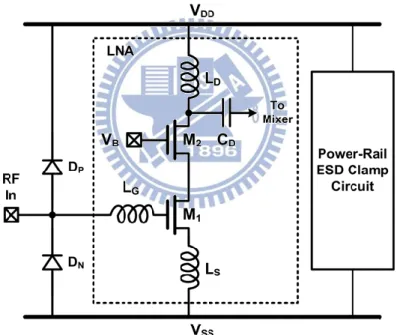
with the concepts of S-parameters can help us. A conventional double-diode ESD protection
design with a power-rail ESD clamp circuit for LNA is shown in Fig. 2.15.
Fig. 2.15. Conventional ESD protection design with double diodes and a power-rail ESD
clamp circuit for LNA.
In the circuit in Fig. 2.15, the parasitic effects of ESD protection diodes, DP and DN,
cause RF performance degradation. Some equations can be calculated to describe the impact
21 0 21, 1 1 2 ESD ESD ESD Z IL Z S (2.20)
where Z0 is the 50-Ω normalization impedance, and ZESD is the parasitic impedance of ESD
protection diodes at the input node. Using the expression in dB, the insertion loss (ILESD) is
equal to the absolute value of S21 parameter (S21, ESD).
The power gain of an RF LNA with ESD protection devices can be calculated from its
schematic circuit diagram, as shown in Fig. 2.16. A simple expression of the input impedance
(Zin, LNA) of LNA at resonance is [12]
, 0 1 ( ) ( ) in LNA s g s T s gs gs gm Z s L L L L Z sC C (2.21)
where T is the unity-gain frequency of the MOS transistor. The overall input impedance (Zin)
of the LNA with ESD protection diodes is
Zin ZESD//Zin LNA, ZESD//Z0 (2.22)
Therefore, the overall transconductance (Gm) of the LNA is
0 0 0 0 1 ( ) 2 ESD T T m ESD in ESD Z G Z Z Z s Z Z sZ Z (2.23)
The transducer power gain of the LNA can also be calculated. In order to simplify the
calculation, the feedback capacitor Cgd of the MOS transistor was neglected first, and the
input and output were assumed to be conjugately matched. The transducer power gain (GT) is
2 2 0 0 2 2 2 0 0 0 1 / / / / 8 4 1 8 s m o T o L T avs s ESD V G R Z R Z P G P V Z IL Z (2.24)where PL is the average power delivered to the load, Pavs is the average power available from
the source, Ro is the output impedance of the cascoded NMOS transistors, and 0 is the
22
Fig. 2.16. LNA with parasitic impedance of input pad and ESD protection diodes for
calculating the power gain.
The calculations demonstrate the disadvantages to the transducer power gain of LNA. It
is caused by the insertion loss of ESD protection diodes. If the parasitic impedance of ESD
protection diodes (ZESD) can be increased to infinite, the transducer power gain of LNA in Fig.
2.16 would converge to that of an LNA without any ESD protection diode. Therefore, ESD
protection device with high parasitic impedance, namely, low insertion loss, is needed for RF
ESD protection.
2.4.2 Challenges of RF ESD Protection Design
Once the parasitic impedance of ESD protection diodes can be increased, the degradation
of RF performance of LNA would be improved. Reducing the device dimensions of ESD
protection diodes can increase (decrease) the parasitic impedance (capacitance). Hence, the
RF performance degradation caused by ESD protection diodes would be reduced.
Unfortunately, such demand is on the opposite side of the demand of ESD robustness. The
23
ESD robustness. Moreover, the ZESD will further decrease as the operating frequency of RF
circuits increases. Designing an effective ESD protection design for RF circuits operating in
higher frequency with minimum RF performance degradation is a terrible dilemma.
2.4.3 Conventional RF ESD protection designs
To overcome these problems, many RF ESD protection designs have been developed.
One method is trying to cancel or isolate the parasitic capacitances from RF circuits, such as
“ESD cancellation” and “ESD isolation”; other method is trying to fundamentally reduce the parasitic capacitances of ESD protection devices in order to minimize the influence on RF
performance [13] [14]. Some of these methods will be briefly introduced in this section.
“ESD isolation” is a method to protect RF circuits under ESD events, and “isolate” the parasitic capacitances of ESD protection devices from RF circuits under normal operating
conditions. Well designed “ESD isolation” can provide enough ESD robustness without
serious RF performance degradation. An example is using LC-tanks, as shown in Fig. 2.17 [6].
The impedance of LC-tank is infinite when LC-tank operates at its resonant frequency. For
this reason, the pair of LC-tanks can be designed to resonate at the operating frequency of the
internal RF circuit, and the RF input port will see infinite impedance through ESD clamp
devices with the LC-tank, ideally. Therefore, the parasitic effects of ESD protection devices
would not influence the RF circuit under normal operating conditions. The resonant frequency
of LC-tanks is 0 1 1 P P N N L C L C (2.25)
24
Fig. 2.17. ESD protection design with LC-tanks for RF circuits.
Another method is using series inductor and diode as ESD protection device, as shown in
Fig. 2.18 [5]. The diode can be considered as a capacitor because of its parasitic effect. The
impedance of the series inductor and diode is extremely small when the two devices operate at
their resonant frequency, but extremely high when the two devices operate at frequencies
above the resonant frequency. The resonant frequency of the series inductor and capacitor is the same as (2.9). Choose the resonant frequency of the series inductor and diode far away
from the operating frequency of the RF circuit, and therefore the RF input port can see infinite
impedance through the series inductor and diode under normal operating conditions. Thus, the
parasitic effects of ESD protection devices would not influence the RF circuit. Of course, the
25
Fig. 2.18. ESD protection design with series diodes and inductors for RF circuits.
“ESD cancellation” is a method to turn ESD protection devices into a part of RF circuit so as to “cancel” the parasitic capacitances introduced by ESD protection devices.
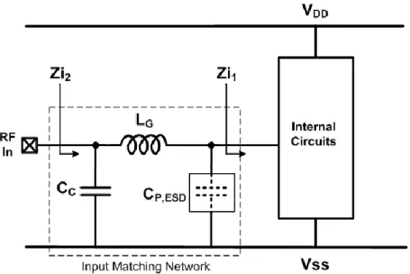
A commonly used method is considering ESD protection devices as parts of matching
network [15]. If an ESD protection device is simply added in front of an RF circuit, the
parasitic capacitance of the ESD protection device might change the input matching condition.
Merging the ESD protection device into the input matching network can minimize the
influence. Fig. 2.19 shows this method. CP,ESD is the parasitic capacitance of an ESD
protection device which changes the input matching condition. By adding extra capacitor CC
and inductor LG, the input impedance of the internal RF circuit can be changed from Zi1 to Zi2
of 50Ω. Hiding ESD protection devices in input matching network can cancel the RF
26
Fig. 2.19. Input matching co-design of RF circuits with ESD protection devices.
In addition, this method can be extended to broadband RF applications [16], as shown in
Fig. 2.20. The ESD protection devices, which are diodes here, are allocated with decreasing
size from the I/O pad to the internal RF circuit. The ESD protection devices are divided into
several small devices rather than one large device for broad-band RF performance. For ESD
robustness, dividing the ESD protection devices into decreasing size is better than dividing
them into equal size, since a larger ESD protection device inserted right beside the I/O pad is
beneficial to providing a high-current-tolerant ESD discharge path under ESD events. Z0
represents the impedance of transmission lines, coplanar waveguides, or inductors which are
used to do input matching. This architecture successfully combines ESD protection devices
with input matching network, and it can provide enough ESD robustness without serious RF
27
Fig. 2.20. ESD protection devices with decreasing size for broad-band RF circuits.
The methods mentioned above are a little complex to RF circuit designers since ESD
protection circuits have to be co-designed with RF circuits. Considering ESD protection
designs throughout RF design phase needs more effort. Therefore, a more straightforward
direction is to fundamentally decrease the parasitic capacitances of ESD protection devices.
RF designers can therefore easily add low-C ESD protection devices to RF circuits without
complex co-design methodology. To meet these requirements, silicon-controlled rectifier
(SCR) can serve. With well ESD robustness within a small layout area and lower parasitic
capacitance, SCR is useful to RF ESD protection design [8].
Fig. 2.21 shows the cross-section view and the equivalent circuit of a typical SCR. The
SCR structure consists of P-plus (P+) diffusion, N-well, P-well, and N-plus (N+) diffusion, as
shown in Fig. 2.21 (a). This four-layer structure can be regarded as a two-terminal device
28
(a)
(b)
Fig. 2.21. The (a) cross-section view and (b) equivalent circuit of a typical SCR.
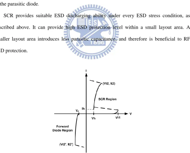
The DC I–V characteristics of SCR under ESD stress is shown in Fig. 2.22. Assume that
positive ESD stress is applied to the anode of SCR and its cathode is relatively grounded. At
the beginning, the voltage applied to the anode is less than the breakdown voltage of the
N-well/P-well junction, so SCR acts like an open circuit. When the voltage applied to the
anode is greater than the breakdown voltage, avalanche breakdown mechanism starts to work.
29
meanwhile electron current flows through the N-well to the N+ diffusion connected to the
anode. Once the voltage drops across the P-well resistor (RP-well) (N-well resistor (RN-well)) is
larger than 0.7 V, the parasitic NPN (PNP) transistor will be turned on. Furthermore, the
parasitic NPN (PNP) transistor injects electron (hole) current to bias the PNP (NPN) transistor,
and then the positive-feedback regenerative mechanism helps SCR to be successfully
triggered into its latching state and have a low holding voltage (Vhold) ~1.5 V.
Next, assume that negative ESD stress is applied to the anode of SCR and its cathode is
relatively grounded. This negative voltage drops across the parasitic diode, which consists of
the P-well/N-well junction, in SCR. As long as the parasitic diode is forward biased, ESD
current can be discharged and the negative voltage will be clamped at the low cut-in voltage
of the parasitic diode.
SCR provides suitable ESD discharging ability under every ESD stress condition, as
described above. It can provide high ESD protection level within a small layout area. A
smaller layout area introduces less parasitic capacitance, and therefore is beneficial to RF
ESD protection.
Fig. 2.22. I–V characteristics of SCR device under positive and negative voltage biases.
30
Chapter 3
ESD Protection Design for 60 GHz RF Circuits
3.1 Challenges of ESD Protection Design for 60 GHz RF Circuits
To design an ESD protection design for 60 GHz RF Circuits, a crucial problem needs to
be concerned. The impedance of an ESD protection device can be expressed as
1 ESD ESD Z sC (3.1)
The higher the operating frequency is, the lower the impedance of ESD protection device is. Low impedance causes large signal loss, and therefore causes serious RF performance
degradation. Since the operating frequency of 60 GHz RF circuits is pretty high, the parasitic
capacitance of ESD protection device needs to be extremely suppressed. However, extremely
suppressing the parasitic capacitances of ESD protection devices such as SCR to fit the
requirement of 60 GHz RF circuits is difficult. Thus, low-C ESD protection device may not
be a good option.
ESD isolation would be a proper method, since the limitation of the parasitic capacitance
of ESD protection device is not that tough, and it would not increase the design complexity of
RF circuits. Nevertheless, the drawback of the ESD isolation method shown in Fig. 2.17 is its
high clamping voltage. The clamping voltage of the ESD protection design under ESD stress
conditions is the sum of the clamping voltages of LC-tank and ESD protection diode. It is
31
3.2 Architecture of The Proposed ESD Protection Designs
Fig. 3.1 shows the circuit of one proposed ESD protection design for 60 GHz RF circuits.
The ESD protection design A, which consists of a pair of ESD protection diodes (DP and DN),
a series inductor and capacitor (LN and CN), and a supplement capacitor (CS), is placed beside
the I/O pad. The diodes provide ESD discharge paths from the input pad to VDD / VSS. In
addition, a power-rail ESD clamp circuit is placed between VDD and VSS power lines so as to
provide a discharge path between VDD and VSS.
The inductor in series with the capacitor can block the dc leakage path from input pad to
VSS under normal operating conditions. The equivalent inductance of the series inductor and
capacitor (Leq) can be expressed as
2 1 eq N N L L C (3.2)
Leq can be used to eliminate the parasitic capacitance of ESD protection diodes (CDiodes) at the
operating frequency of the RF circuit by careful design. The resonant frequency of the parallel
Leq and CDiodes is designed to be equal to the operating frequency of the RF circuit. Under this
condition, the RF input port will see a large impedance from the ESD protection circuit (ZESD),
where the parasitic capacitance (CDiodes) has been eliminated, and the parasitic resistance
(RDiodes) remains large.
The resonant frequency of parallel Leq and CDiodes can be calculated by
0
1
eq Diodes L C
(3.3)
From Eq. (3.2) and (3.3), another equation is obtained as
2 0 1 1 N N Diodes L C C (3.4)
32
determined, (3.4) can be used to find the required inductance and capacitance. Besides, the
resonant frequency of the series inductor and capacitor should be far away from the operating
frequency, since the impedance would be extremely small at its resonant frequency. The
resonant frequency of LN and CN (Series) can be calculated as
1 Series N N L C (3.5)
To investigate the ESD robustness of ESD protection designs with different sizes of ESD
protection diodes, several splits with DN and DP in different sizes are studied. Since the CDiodes
varies with the size of ESD protection diode, a supplement capacitor (CS) is added between
RF input and VSS to keep the total capacitance of CDiodes and CS. Therefore, the sizes of LN
and CN can maintain the same, and the layout area can also maintain the same. Consider
CDiodes and CS as one capacitor, and (3.4) turns out to be
2 0 ESD 1 1 N N L C C (3.6) where CESD is ESD Diodes S C C C (3.7)
The power-rail ESD clamp circuit consists of an RC-detector, a CMOS inverter, and an
RC-inverter-triggered NMOS. The RC-detector is designed to distinguish ESD transients
from normal operating conditions. The R1 (~10 kΩ) and C1 (~10 pF) with time constant of 0.1
μs ~ 1 μs can meet such requirement, since the rise time of turn-on events are on the order of millisecond whereas that of ESD events are on the order of nanosecond. The NMOS (MESD)
33
Fig. 3.1. Proposed ESD protection design A with supplement capacitor and power-rail ESD
clamp circuit.
Another proposed ESD protection design is shown in Fig. 3.2. The ESD protection design
B also consists of a pair of ESD protection diodes (DP and DN), but the series inductor and
capacitor (LP and CP) are placed between RF input and VDD. The operation of design B is
similar to design A, and the design parameters can be calculated with (3.2) by replacing the
LN by LP.
34
3.3 ESD Discharge Paths of the Proposed ESD Protection Designs
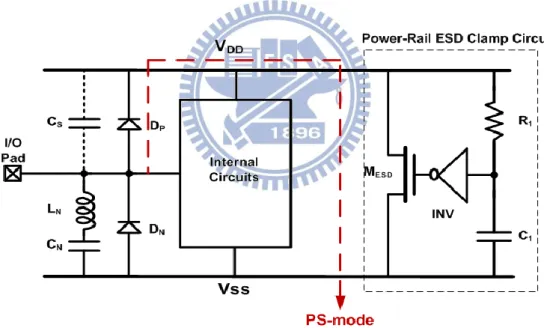
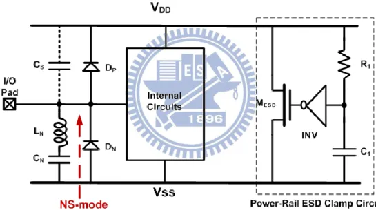
With this architecture, proper ESD discharge paths under every ESD zapping mode are
guaranteed. For PS-mode, the ESD current first goes through DP, and then it is discharged
through the power-rail ESD clamp circuit. For PD-mode, the ESD current is discharged
through DP. For NS-mode, the ESD current is discharged through DN. For ND-mode, the ESD
current is first shunted from VDD to VSS through the power-rail ESD clamp circuit and then
discharged through DN. For VDD-to-VSS and VSS-to-VDD mode, the power-rail ESD clamp
circuit can provide ESD discharge paths. All the ESD discharge paths are shown in Figs. 3.3
to 3.7. The proposed designs A and B have the same ESD discharge paths.
35
Fig. 3.4. ESD discharge path of the proposed design A under PD-mode.
36
Fig. 3.6. ESD discharge path of the proposed design A under ND-mode.
Fig. 3.7. ESD discharge path of the proposed design A under VDD-to-VSS and VSS-to-VDD
mode.
Since the ESD current is discharged through only one diode from I/O pad to power lines,
the clamping voltage under ESD stress conditions is lower than that of the structure shown in
Fig. 2.17. It is beneficial to its ESD protection ability.
37
3.4 Simulation Results
The proposed designs are simulated by using ideal lumped devices. A 0.11-nH inductor
and a 300-fF capacitor are used as the series inductor (LN) and capacitor (CN). The diodes DN
and DP are simplified to an ideal capacitor model, CDiodes. The sum of CDiodes and CS, that is,
CESD in (3.6), is chosen as an 80-fF capacitor. Since ideal devices are used, the proposed
designs A and B have the same simulation results. The simulated S21 parameter (S21, ESD) of
the proposed design is shown in Fig. 3.8. The S21 value at 60 GHz can be designed to be 0 dB,
which means that insertion loss from ESD protection circuit is also 0 dB.
Fig. 3.8. Simulated S21 parameter of the proposed design.
3.5 Experimental Results
3.5.1 Test Circuits
Increasing device sizes of ESD protection diodes provides better ESD robustness but
worse RF performance, and decreasing device sizes of ESD protection diodes makes opposite
38
designs are split into 4 test circuits with different sizes of ESD protection diodes. The test
circuits of the proposed ESD protection designs have been fabricated in a 65-nm CMOS
process. All device sizes are listed in Table 3.1. The width of DP or DN in test circuits A1 (B1),
A2 (B2), A3 (B3), and A4 (B4) are 8 m, 15 m, 23 m, and 30 m, respectively, while the length of DP or DN are kept at 0.6 m. The CDiodeds of test circuits A1 (B1), A2 (B2), A3 (B3),
and A4 (B4) are 21 fF, 40 fF, 61 fF, and 80 fF, respectively. The LN and LP are chosen as 0.11
nH for designs A and B, and the CN and CP are designed as 300 fF. Besides, the CS with 60 fF,
40 fF, and 20 fF are added to the test circuits A1 (B1), A2 (B2), and A3 (B3), respectively. To
facilitate the on-wafer RF measurement, these test circuits are arranged with G-S-G style in
layout. Part of the layout top view of the test circuit A4 is shown in Fig. 3.9. In other splits, CS
was added beside DN. Every test circuit has the same layout area, 130×100 m2, as A4 does,
since almost the same components are used in every test circuit. Table 3.1
Device Parameters of Proposed ESD Protection Designs
Test
Circuit
Proposed Design A Proposed Design B
A1 A2 A3 A4 B1 B2 B3 B4
LP N/A N/A N/A N/A 0.11 nH 0.11 nH 0.11 nH 0.11 nH
CP N/A N/A N/A N/A 300 fF 300 fF 300 fF 300 fF
DP 8 m × 0.6 m (9 fF) 15 m × 0.6 m (18 fF) 23 m × 0.6 m (27 fF) 30 m × 0.6 m (36 fF) 8 m × 0.6 m (9 fF) 15 m × 0.6 m (18 fF) 23 m × 0.6 m (27 fF) 30 m × 0.6 m (36 fF)
LN 0.11 nH 0.11 nH 0.11 nH 0.11 nH N/A N/A N/A N/A
CN 300 fF 300 fF 300 fF 300 fF N/A N/A N/A N/A
DN 8 m × 0.6 m (12 fF) 15 m × 0.6 m (22 fF) 23 m × 0.6 m (34 fF) 30 m × 0.6 m (44 fF) 8 m × 0.6 m (12 fF) 15 m × 0.6 m (22 fF) 23 m × 0.6 m (34 fF) 30 m × 0.6 m (44 fF) CS 60 fF 40 fF 20 fF N/A 60 fF 40 fF 20 fF N/A
39
Fig. 3.9. Layout top view of the test circuit A4.
3.5.2 Measured RF Performance
The two-port S-parameters of the test circuits from 0 to 67 GHz were measured by using the
vector network analyzer. During the S-parameter measurement, the port 1 and port 2 were
biased at 0.5 V, which is VDD/2 in the given 65-nm CMOS process. The dc bias of 1-V VDD
was also supplied to the test circuits.In order to extract the intrinsic characteristics of the test
circuits in high frequencies, the parasitic effects of the G-S-G pads had been removed by
using the de-embedding technique [17]. The source and load resistances to the test circuits
were kept at 50 Ω.
The measured S21 parameters of the test circuits are shown in Figs. 3.10 and 3.11. For the
proposed design A, the test circuits A1, A2, A3, and A4 have about 1.3-dB, 1.4-dB, 1.6-dB,
and 1.8-dB insertion loss, respectively, at 60-GHz. For the proposed design B, the test circuits
B1, B2, B3, and B4 have about 1.4-dB, 1.6-dB, 2.0-dB, and 2.3-dB insertion loss, respectively,
at 60 GHz. Since the diodes used in simulation are simplified to ideal equivalent capacitor
models rather than real diode models, the measured signal loss were larger than the simulated
signal loss. The insertion loss of the proposed design B seems a little bit larger than the
40
noise figures are also measured at 60 GHz. For design A, the test circuits A1, A2, A3, and A4
have 0.9-dB, 1.2-dB, 1.6-dB, and 2-dB noise figures, respectively. For design B, the test
circuits B1, B2, B3, and B4 have 0.9-dB, 1.3-dB, 1.7-dB, and 2.2-dB noise figures,
respectively.
(a)
(b)
Fig. 3.10. Measured S21 parameters of proposed design A within (a) 0~67 GHz and (b)
41
(a)
(b)
Fig. 3.11. Measured S21 parameters of proposed design B within (a) 0~67 GHz and (b)
42
3.5.3 Measured ESD Robustness
ESD robustness of every ESD test circuit is evaluated by ESD tester. For the HBM ESD
robustness, each test circuit is zapped by ESD pulses under PS-mode, PD-mode, NS-mode,
and ND-mode ESD stress conditions. The failure criterion is defined as the I-V characteristics
seen at RF input shifting over 30% from its original curve. The PS-mode, PD-mode, NS-mode,
and ND-mode HBM ESD robustness of all ESD test circuits are measured, as listed in Table
3.2. According to the test results, the HBM ESD robustness of the proposed designs can be
obtained from the lowest level of the robustness of the four modes. For the proposed design A,
the test circuits A1, A2, A3, and A4 have 0.25-kV, 1.25-kV, 1.75-kV, and 2-kV HBM ESD
robustness, respectively. For the proposed design B, the test circuits B1, B2, B3, and B4 have 0.25-kV, 1.25-kV, 1.75-kV, and 2.25-kV HBM ESD robustness, respectively. The measurement results of RF performance are also summarized in Table 3.2, inclusive of the
measured S11 parameters. The measured S11 parameters show that all test circuits exhibit good
43
Table 3.2
Comparisons of Experimental Results Among ESD Protection Circuits in Silicon
Proposed Design A Proposed Design B [18]
A1 A2 A3 A4 B1 B2 B3 B4 S11 Parameters at 60 GHz -16 dB -17 dB -19 dB -21 dB -22 dB -29 dB -26 dB -26 dB -22 dB S21 Parameters at 60 GHz -1.3 dB -1.4 dB -1.6 dB -1.8 dB -1.4 dB -1.6 dB -2.0 dB -2.3 dB -2.1 dB Noise Figures at 60 GHz 0.9 dB 1.2 dB 1.6 dB 2.0 dB 0.9 dB 1.3 dB 1.7 dB 2.2 dB - PS-Mode HBM ESD Robustness 0.25 kV 1.5 kV 1.75 kV 2 kV 0.25 kV 1 kV 1.75 kV 2.25 kV 2.5 kV PD-Mode HBM ESD Robustness 0.25 kV 1.5 kV 2.25 kV 2.5 kV 0.25 kV 1.5 kV 2.25 kV 2.5 kV 3.5 kV NS-Mode HBM ESD Robustness 0.5 kV 1.25 kV 2 kV 2.25 kV 0.5 kV 1 kV 1.75 kV 2.25 kV 2.75 kV ND-Mode HBM ESD Robustness 0.25 kV 1.25 kV 2 kV 2.25 kV 0.25 kV 1 kV 1.75 kV 2.25 kV 2.75 kV Layout Area 100×130 m2 100×130 m2 100×130 m2 100×130 m2 100×130 m2 100×130 m2 100×130 m2 100×130 m2 110×220 m2
3.5.4 Comparison and Discussion
The HBM ESD robustness and the measured S21 parameters at 60 GHz of the proposed
ESD protection designs A and B are compared in Table 3.2. Among the splits of the proposed
designs A and B, the test circuit A4 (B4) can achieve 2-kV HBM ESD robustness with 1.8-dB
(2.3-dB) insertion loss. Since the signal loss of B4 is a little higher than that of A4, A4 is the
suitable ESD protection design for 60 GHz RF circuits in these splits.
There is another reference ESD protection design, which is also applied on 60 GHz RF
circuits and had been verified in a 65-nm CMOS process, is compared with the proposed
44
passive devices - two diodes and two inductors. The drawback is its large layout area.
Compared with the reference design, the layout area of the proposed designs can be reduced
from 110×220 m2 to 100×130 m2. Moreover, the test circuit A4 can provide the required 2-kV HBM ESD robustness with lower insertion loss. Therefore, the compact ESD protection
circuit for 60 GHz RF circuits can be realized by using the test circuit A4. The proposed