flipflop 2 flipflop 1 I 0 CLK
--
CLKI
+I
D1 D2 03 0 F R E Q I N D MODE D MODE: 0--
-
DI D2 0-
=
Fig. 4 Dual-modulus divider 4/3
Conclusions: The realisation of dual-modulus frequency dividers with minimum gate count has been addressed in a general way. An expression for the maximum number of different (Wk+l) dividers was derived. This number is equal to the number of dif- f m n t state-mapping sets of Boolean equations. A computer search for a mapping-set containing one type of Boolean operator only was performed. Equation sets for divide-by-2/3 and divide-
b y 4 5 have been presented. A D-flipflop with multiple inputs was used as a building block in the realisation of these dividers. Detailed schematic diagrams for divide-by-U3 and divide-by45 frequency dividers using NOR-gates have been presented. Speed
increase and power savings in dual-modulus frequency dividers have been achieved by reducing the gate count.
0 IEE 1994
Electronics Letters Online No: 19940829
P. Wennekers (Motorola Inc., Semiconductor Product Sector, 2100 East Elliott Road, Tempe, Arizona 85284. USA)
6 June 1994 ~ FREQIN CLK MODE
-
D 1 0 MOOLO- Refereaees1 OHATA. M., TAKADA, T., INO. M., KATO, N., and IDA, M.: ‘A 4.5-Ghz GaAs dual-modulus prescaler IC‘, IEEE Trans.. 1988, MTT-36, pp, 158-160
2 KASAHARA, I., WADA, M., KAWASAKI. H., HIDA, Y., and OKUBORA, A.: ‘IO GHz GaAs JFET dual-modulus prescaler IC‘, Elecrron. Lett.,
1989,2S, pp. 889-890
3 MIZUNO, M., SUZUKI, H., WAWA, M., SATO, K., and ICHIKAWA, H . : ‘A 3-mW I.0-GHz silicon-ECL dual-modulus prescaler IC’, IEEE J. Solid-State Circuits, 1992, SSC-27, pp. 17941798
4 SENEFF, T., MCKAY. L., SAKAMOTO, K., and TRACHT, N.: ‘A sub-lmA 1.SGHz silicon bipolar dual modulus prescaler’. IEEE, BCTM- Proc. Minneapolis, 1993, pp. 24S243
5 KADO, Y., SUZUKI, M., KOIKE, K., OMURA, Y . , and IZUMI, K.: ‘A 1-
GHd0.9mW CMOS/SIMOX divide-by-128/129 dual-modulus prescaler using a divide-by-2/3 synchronous counter’, IEEE J. Solid-state Circuits, 1993, SSC-28, pp. 513-517
__
-
CLK CLK
D Q o ! G DFREQ
-
-Ll
Genetic algorithms for the module
orientation problem
R.-I.
Changand
P.-Yung HsiaoIndexmr t e r n : Circui) bvout CAD. Geneti alaorithm
To solve the module orientation problem the optimal number of
!lips of modules needs to be determined so as to minimix total
wire length. A geneticbased module orientation metbod is proposed. Experiments show that the proposed method performs
better than the best method known for this problem.
ELECTRONICS LETTERS
21stJuly
1994Vol.
30
Introduction: The placement of modules to minimise total wire length is a major consideration in the physical design of VLSI cir-
cuits. Assume that the modules have already been placed by some placement algorithms and the pin positions on each module are fxed on the module boundary. An improvement can be. made to further minimise total wire length by flipping these modules with respect to their vertical and/or horizontal axes of symmetry. The problem of fmding the optimal flip for a given set of modules with minimium total wire length is called the module orientation problem. It has been proved to be NP-complete [I] for macro-cell layout, and some methods were presented in [I-41. In 1992, a neu- ral-based module orientation method was presented by Lee and Takefuji [2] using a generalised maximum neural network. To our knowledge, it is the best algorithm known for this problem. In this Letter, a new approach based on a natural processing concept is proposed to minimise total wire length for the module orientation problem. The presented method, which mimics the mechanics of natural selection and genetics, is called a genetic algorithm
[q.
The algorithm starts with an initial set of random configuratons and uses a process similar to biological evolution to improve on them. Because of its robustness and effec!iveness, this method has been successfully applied in various optimisation problem. In this Let-ter, a genetic-based module orientation method is proposed. Experiments show that it performs better than the best algorithm [2] !mown for this problem. Moreover, the proposed approach which uses the concept of evolution is capable of handling differ- ent wire-length metrics and more complicated problem constraints.
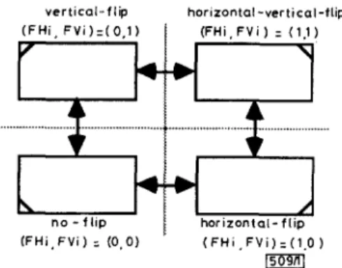
v e r t i c a l - f l i p horizontal - v e r t i c a l - f l i p ( F H i , F V i )
=
(1.1) /I
( F H i . F V i I = ( 0.1) \ ( F H i , F V i )=
(0,O) ( F H I , F V i ) (1.0 )Fig. 1 No-&, horizontal fl@, vertical flip and horizontal-vertical
fl@
states of circuit module
rn
Formulations f o r module orientation problem: Assume that each cir-
cuit module i has an orientation state ( F H j ,
Fu
where FK andFHE E {0, 1) represent the states of vertical flip and horizontal flip, respectively. Thus, the orientation states (FH,,
m)
= (0, 0),(I, 0), (0, 1) and (1, l), as shown in Fig. 1, denote no-flip, horizon- tal-flip, vertical-flip and horizontal-vertical-flip of the circuit mod- ule, respectwely. Assume that there are n Circuit modules and each circuit module i has already been placed with centre (xt, yJ. Let pin j located on a macro-cell i be fmed on the module boundary with position (x,,, yJ The offset (dx,,, dyjj) can be defined as
(x, - x,, y, - y j ) . It is clear that the co-ordinates (xc
+
Ajj, y,+
are the positions of the pm j by no-flip, horizontal-flip, vertical- flip and horizontal-vertical-flip of module i, respectively. In this Letter, we simply rewrite the pin position as(x,,
y,)
= (x,+
(1 -2FHi) x Ajj, y ,
+
(1 - 2m.) x dyjj). Assume that there are m wire nets in the problem, and each wire net k is connected from pin Po, of module MO, to pin P1, of module MI,; then, the total wire length can be defined as follows:&,),
- ei.3~i + dy,),(xi
+ d . j , Y , - dyzj) and (x; - &I, Y? - &,,)In
J(XA4OlrPOI - XA4lkPl,)2
+
(YA401POk - YMlLPlk)2k = l
(1) The module orientation problem is defmed to minimise the total wire length by flipping circuit modules.
Module flipping using genetic algorithms: A genetic algorithm is presented to minimise the objective function as eqn. 1. Typically, the set of configurations on which the genetic algorithm operates
is called the population. Each individual in the population is a
binary bit string (called chromosome) representing a solution to
the problem. During each iteration, called a generation, the indi- viduals in the current population are evaluated, using some meas-
ure of fitness called a fitness function. Based on this fitness value, individuals are selected from the population as parents. A number of genetic operators (i.e. crossover and mutation) are applied to the parents for generating new individuals, called offspring. The offspring are next evaluated, and a new generation is formed by selecting some of the parents and offspring, and rejecting others so
as to keep the population size constant.
Thus,
the evolution results of an optimal individual will lead to an optimal solution for the problem. The flip of circuit module i is represented by the orienta-tion state ( F e ,
w).
In this Letter, the solution configuration of the proposed problemcan
be binary encoded into the chromo- some(FHIFV,FH,FV,
...
FH#FV.). We &me the fitness function to evaluate the individuals as -1 x eqn. 1. Thus, the evolution results of an optimal chromosome will lead to the optimal orienta- tion assignments for macro-cell placement. The module orienta-tion problem can be solved by a genetiebased algorithm. A simple example to demostrate this idea is shown in Fig. 2.
3
11 10t
2
0 VI 111 0 1lJ1
11011509/21
Fig. 2 Simple example to demonstrate proposed genetic-based method
- 3 0 r
-
”\.
5
;
-3 4 x -3 -2-
c VI C c L 0 1 2 3 4 5 6 7 8 9 10 generat ionsrn
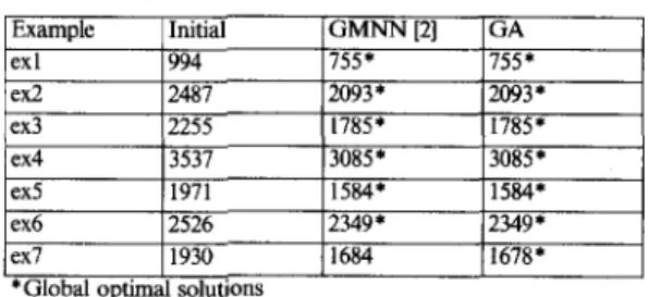
Fig. 3 Fitness of best chromosomes in population for evolution process of ex4generally better than GMNN which cannot find the global opti-
mal solutions for the test example ex7.
Table 1: Comparisons of proposed GA method with GMNN
*Global optimal solutions
Conclusion; A genetiebased module orientation method has been proposed. We have shown that the proposed method is very efi- cient at minimising total wire length by flipping circuit modules. Experiments show that the genetic algorithm yields results better than the previous module orientation methods, both in the fmal result quality and computation time required.
0 IEE 1994
Electronics Letters Online No: 19940837
R:I. Chang and P.-Y. Hsiao (Department of Com uler and Information Science, National Chiao Tung University, Hsinctfu, Taiwan 30050, Republic of China)
I 3 June 1994
References
1 HADAS. R.L., and LIU, C.L.: ‘Solution to the module orientation and rottnion problem by neural computation networks’. Proc. 26th Design Automation Conf., 1989, pp. 40&405
2 LEE, K.c., and TAKEFuJI. Y.: ‘A generalized maximum neural network for the module orientation problem’, Int. J. Electron.. 1992, 72, (3), pp. 331-355
3 YAMADA, M., and LIU, C.L.: ‘An analytical method for optimal module orientation’. Proc. Int. Symp. on Circuits and Systems, 1988, pp. 1679-1682
4 CHENG, c.K., HU. T.c., and YAO. s.z.: ‘The modular orientation of VLSI layout’. Int. Symp. on Circuits and Systems, 1990, pp. 160s 1603
5 GOLDBERG, D.E.: ‘Genetic algorithms in search, optimization and machine learning’ ( M A Addison-Wesley, 1989)
Bandwidth efficient modulation with
wavelets
F. Daneshgaran a n d
M.
MondinIndexina t e r n : Modulation, Wavelet tramforms Experimental results: A genetic algorithm with the size of popula-
tion set 100 and the number of generation 10 is applied. To bench-
mark the performance of the proposed algorithm, the test examples are all taken from [2]. AU our experiments were carried out on a Sun SPARC IPC workstation and the best solutions chosen. Consider a test example ex4 with 10 circuit modules, the total number of configurations examined by the proposed algo- rithm is more than 100 times less than that for the exhaustive search, and the run time was marginally better. Fig. 3 shows the
fitness of the best chromosomes in the population at each genera- tion for the evolution process of ex4. The comparisons of the pro- posed genetic algorithm (GA) method with the generalised maximum neural network (GMNN) are shown in Table 1. To our knowledge, it is the best algorithm known for this problem. Exper- imental results indicate that the proposed genetic-based approach finds the global optimal solutions for all these test examples. It is
The authors demonstrate that the use of scaling functions and wavelets as envelope functions for modulation is natural in view of the fmt Nyquist criterion for IS1 removal. Using wavelet packets, the number of dimensions available to the modulator per
unit time is increased.
Introducfiont Consider Fig. 1 depicting the complex baseband equivalent model of a narrowband communication system. At each time slot the sourn emits a symbol drawn from the complex
plane that linearly modulates the possibly complex shaping pulse whose Fourier transform is So. Simply put, we propose the use of scaling functions and wavelets as this shaping pulse and investi- gate the possibility of approaching the dimensionality limit in the process. The focus of this Letter will be on the Daubechies com-
pactly supported wavelets [l] (the concept presented generalises to other orthonormal wavelets).