Effect of antimony incorporation on the density, shape, and luminescence of InAs
quantum dots
J. F. Chen, C. H. Chiang, Y. H. Wu, L. Chang, and J. Y. Chi
Citation: Journal of Applied Physics 104, 023509 (2008); doi: 10.1063/1.2959598 View online: http://dx.doi.org/10.1063/1.2959598
View Table of Contents: http://scitation.aip.org/content/aip/journal/jap/104/2?ver=pdfcov Published by the AIP Publishing
Articles you may be interested in
Interface properties of InAs quantum dots produced by antimony surfactant-mediated growth: Etching of segregated antimony and its impact on the photoluminescence and lasing characteristics
Appl. Phys. Lett. 94, 103116 (2009); 10.1063/1.3099902
Structural and optical properties of InP quantum dots grown on GaAs(001) J. Appl. Phys. 101, 073508 (2007); 10.1063/1.2718869
High density In As Ga As quantum dots with enhanced photoluminescence intensity using antimony surfactant-mediated metal organic chemical vapor deposition
Appl. Phys. Lett. 89, 183124 (2006); 10.1063/1.2385209
Topological characteristics of InAs quantum dot with GaInAs cover using Sb surfactant Appl. Phys. Lett. 88, 183109 (2006); 10.1063/1.2200395
Sb surfactant effect on GaInAs/GaAs highly strained quantum well lasers emitting at 1200 nm range grown by molecular beam epitaxy
J. Appl. Phys. 96, 44 (2004); 10.1063/1.1760841
共QDs兲 by incorporating Sb into the QD layers with various Sb beam equivalent pressures共BEPs兲. Secondary ion mass spectroscopy shows the presence of Sb in the exposed and buried QD layers with the Sb intensity in the exposed layer substantially exceeding that in the buried layer. Incorporating Sb can reduce the density of the exposed QDs by more than two orders of magnitude. However, a high Sb BEP yields a surface morphology with a regular periodic structure of ellipsoid terraces. A good room-temperature photoluminescence 共PL兲 at ⬃1600 nm from the exposed QDs is observed, suggesting that the Sb incorporation probably improves the emission efficiency by reducing the surface recombination velocity at the surface of the exposed QDs. Increasing Sb BEP causes a blueshift of the emission from the exposed QDs due to a reduction in the dot height as suggested by atomic force microscopy. Increasing Sb BEP can also blueshift the⬃1300 nm emission from the buried QDs by decreasing the dot height. However, a high Sb BEP yields a quantum well-like PL feature formed by the clustering of the buried QDs into an undulated planar layer. These results indicate a marked Sb surfactant effect that can be used to control the density, shape, and luminescence of the exposed and buried QDs. © 2008 American Institute of Physics.
关DOI:10.1063/1.2959598兴 I. INTRODUCTION
Self-assembled InAs quantum dots 共QDs兲1–14 are of great interest for scientific studies and practical applications. One of the important issues for device applications is the ability to modify the size, shape, and density of the dots. However, the self-assembled Stranski–Krastanov method of growth offers very limited modification. Motivated by the beneficial results of the incorporation of antimony共Sb兲 as a surfactant15–18into a strained InGaAs quantum well共QW兲 to extend the range of emission wavelengths, the incorporation of Sb共Refs.19–23兲 or bismuth24in InAs or in InGaAs QDs has been recently investigated. Matsuura et al.21observed a decrease in the dot density upon the incorporation of Sb in InGaAs QDs and attributed this decrease to an Sb surfactant effect that can extend planar growth and suppress dot forma-tion. A predeposition of dilute Sb before the growth of InAs QDs by metalorganic vapor-phase epitaxy was found to in-crease the dot size.23 Very recently, a long emission wave-length of⬃1.6 m at room temperature has been achieved by capping InAs QDs with 共In兲GaAsSb layer.12–14 This wavelength extension is explained by a development of type-II energy alignment. These experimental results seem to indicate that an incorporation of Sb directly into the QDs can lead to an Sb surfactant effect while an incorporation of Sb into the capping layer of the QDs can extend the emission wavelength. To understand the details of the surfactant ef-fect, we have directly incorporated various amounts of Sb
into buried and exposed InAs QDs and characterized their optical and structural properties using photoluminescence 共PL兲, atomic force microscopy 共AFM兲, and transmission electron microscopy 共TEM兲. Secondary ion mass spectro-scopic共SIMS兲 depth profiling is also used to analyze the Sb distribution.
II. EXPERIMENTS
InAs共Sb兲 QDs were grown on n+-GaAs共100兲 substrates by molecular beam epitaxy using a Riber Epineat machine. The QDs were formed by depositing a 2.72 ML-thick In-As共Sb兲 layer at 485 °C at a growth rate of 0.256 Å/s. Three Sb contents with beam equivalent pressures 共BEPs兲 of 1.4 ⫻10−8, 1.8⫻10−8, and 6⫻10−8 torr, supplied from an Sb cracker, were incorporated into the InAs QD growth. Then, the QDs were capped with a 50 Å In0.15Ga0.85As layer grown at 485 ° C at a growth rate of 1.88 Å/s. These buried QDs are sandwiched between two 0.3-m-thick Si-doped GaAs 共6⫻1016 cm−3兲 layers. For AFM characterizations, similar QDs capped with a 50 Å In0.15Ga0.85As layer were also grown on sample surface. Details of the growth of the QDs can be found elsewhere.22PL measurements were made using a double frequency yttrium aluminum garnet: Nd laser at 532 nm.
III. MEASUREMENT AND RESULTS
Figure1 shows the SIMS depth profiles for Sb BEP of 6⫻10−8 torr. The profiles show the presence of Sb near the sample surface and at a depth of 0.3 m, suggesting a suc-a兲Electronic mail: [email protected].
0021-8979/2008/104共2兲/023509/5/$23.00 104, 023509-1 © 2008 American Institute of Physics
cessful incorporation of Sb in the exposed and buried layers. However, the three dimensional nature of the QDs is such that the detected Sb may not be completely inside the QDs. A significant amount of Sb may be present in the intervening GaAs. Although the exposed and buried layers were grown similarly, the Sb intensity in the exposed layer substantially exceeds that in the buried layer. Similar profile is observed for In intensity. The observed Sb intensity in the exposed layer depends linearly on the Sb BEP, suggesting that Sb can be incorporated into the exposed layer without saturation ef-fect. However, the Sb intensity in the buried layer only slightly exceeds the background Sb noise. Decreasing the Sb BEP further weakens the Sb intensity in the buried layer. For a low Sb BEP of 1.4⫻10−8 torr, the Sb intensity in the buried layer is close to a background level. Because of the very low intensity, no reliable relationship between the BEP and the Sb intensity can be obtained in the buried layer. The low Sb intensity in the buried layer suggests a weak Sb in-corporation. Because Sb concentration is dilute in the buried QDs, the resulting increase in the QD/GaAs lattice mismatch and the decrease in the band gap in the buried QDs due to Sb occupation of As sublattice are considered insignificant.
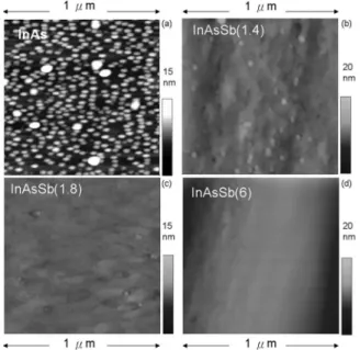
Figures 2共a兲–2共d兲 show the representative 1⫻1 m2 AFM images of the exposed QDs with Sb BEPs of 0, 1.4 ⫻10−8, 1.8⫻10−8, and 6⫻10−8 torr, respectively 关denoted as InAs, InAsSb共1.4兲, InAsSb共1.8兲, and InAsSb共6兲, respec-tively兴. Without Sb, random QDs with a density of 3 ⫻1010 cm−2can be seen along with a few large clusters. An Sb BEP of 1.4⫻10−8 torr can reduce the dot density to 3.5 ⫻109 cm−2; an Sb BEP of 1.8⫻10−8 torr further reduces it to 6⫻108 cm−2. The reflection high-energy electron diffrac-tion patterns show delayed QD formadiffrac-tion upon Sb incorporation.22Therefore, the decrease in dot density is ex-plained by an Sb surfactant effect that can extend two dimen-sional 共2D兲 growth and suppress dot formation. Further in-creasing Sb BEP to 6⫻10−8 torr changes the surface morphology to ellipsoid terraces of height ⬃9 nm, length ⬃4.5 m, and width⬃1.3 m, as shown in Fig.3. Thus, a
large Sb BEP worsens the surface morphology and a signifi-cant amount of the deposited material tends to form these thick terraces, rather than a thin wetting layer. A few QDs are observed on top of these terraces. The dot density is too low to be determined accurately by AFM. However, since the AFM picture shows less than one dot in an area of 1 ⫻1 m2, the estimated density is less than 1⫻108 cm−2. This density is more than two orders of magnitude lower than that of the Sb-free QDs. Cross-sectional TEM reveals a typical dot with a height of about 3 nm and a diameter of 20 nm. This AFM result shows that Sb incorporation can effec-tively reduce the density of the exposed QDs, as previously observed.21 However, increasing the Sb BEP to 6 ⫻10−8 torr yields a surface morphology with a regular pe-riodic structure of ellipsoid terraces.
The density reduction is accompanied by concomitant size and shape modifications. The Sb-free QDs have an av-erage lateral diameter of 50 nm and a height of 10 nm. An Sb BEP of 1.4⫻10−8 torr reduces the height to⬃5 nm without significantly affecting the lateral diameter. Increasing the Sb BEP to 1.8⫻10−8 torr reduces the lateral diameter and height to 35 and 3 nm, respectively. Further increasing the Sb
FIG. 1. SIMS depth profiles of ion intensities for InAs共Sb兲 QDs with Sb BEP of 6⫻10−8 torr. The profiles reveal the presence of Sb in the exposed
and buried QD layers. The intensity in the exposed layer substantially
ex-ceeds that in the buried layer, suggesting Sb segregation at growth front. FIG. 2.共a兲–共d兲 Representative 1⫻1 m2AFM images of the exposed QDs
with Sb BEPs of 0, 1.4⫻10−8, 1.8⫻10−8, and 6⫻10−8 torr, respectively.
Sb incorporation can reduce the dot density by more than two orders of magnitude.
FIG. 3. For a high Sb BEP of 6⫻10−8 torr, the surface morphology
com-prises ellipsoid terraces of height ⬃9 nm, length ⬃4.5 m, and width ⬃1.3 m.
023509-2 Chen et al. J. Appl. Phys. 104, 023509共2008兲
BEP to 6⫻10−8 torr reduces the lateral diameter to⬃20 nm without significantly affecting the height. This dot size re-duction is consistent with the surfactant’s suppression of the growth of the QD and thus the Sb surfactant effect markedly affects the growth of the exposed QDs. Although the lateral dimension is reduced as the Sb BEP increases, the ratio of the lateral diameter to the height exceeds significantly that of the Sb-free QDs and the ratio increases with Sb BEP, and so Sb incorporation can elongate the shape of the QD. These results show a significant Sb surfactant effect affecting the growth of the exposed QDs. The SIMS profile shows a high Sb intensity in the exposed layer and the intensity can be linearly varied by changing the Sb BEP. Thus, this surfactant effect can be utilized for the effective modification of the density and shape of the QDs.
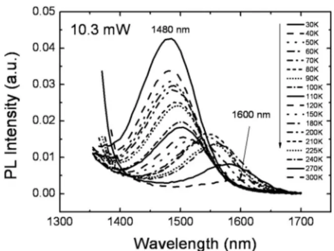
Figure 4 shows the 300 K PL spectra for Sb BEPs of 1.4⫻10−8, 1.8⫻10−8, and 6⫻10−8 torr, respectively. Each spectrum displays two groups of peaks. The peaks at ⬃1300 nm are from the buried QDs and the peaks at ⬃1600 nm are from the exposed QDs since they disappear after slight chemical etching on the sample surface. The PL spectra of Sb-free QDs exhibit a similar 1300 nm emission without the 1600 nm emission. There are two possible con-tributions for the long wavelength in the exposed QDs: strain relaxation and Sb incorporation. Considering a significant compressive strain in the buried QDs, strain relaxation in the exposed QDs11can lead to a wavelength extension. Previous studies have shown that uncapped InGaAs QDs on a GaAs surface could emit a long wavelength near 1500 nm.11 An-other contribution is due to Sb incorporation since the SIMS profile shows a high Sb incorporation in the exposed QD layer than in the buried layer. A high Sb concentration can substantially decrease the band gap of the InAs QDs and result in a wavelength extension. Another possibility is that the incorporated Sb may segregate to the InGaAs capping layer, forming an InGaAsSb capping layer on the QDs. A long wavelength of 1600 nm was previously observed in InAs QDs capping with an共In兲GaAsSb layer due to the for-mation of type-II energy alignment.12–14 Further
investiga-tion is needed to clarify the detailed origin for the wave-length extension. The emission from the exposed QDs is blueshifted from 1617 to 1554 nm as Sb BEP increases. This blueshift is attributed to a reduction in the dot height, as suggested by the AFM observation. Thus, the shift in the PL emission for the exposed QDs as Sb BEP is varied is mainly governed by the surfactant effect. Figure5plots the tempera-ture dependence of ⬃1600 nm emission with Sb BEP of 1.4⫻10−8 torr. As temperature is lowered, the emission in-tensity increases and a blueshift of 63 meV共Varshini rule兲25 is observed, reflecting good emission efficiency for such a long wavelength. Due to strong surface recombination veloc-ity, it is difficult for the exposed QDs to exhibit good emis-sion efficiency. Saito et al.11reported that In segregation on the surface InGaAs QDs could improve PL intensity by re-ducing surface recombination velocity and suppressing car-rier loss at the surface of QDs. However, in our case, the improvement in the emission efficiency shall be related to Sb since no 1600 nm emission was observed in Sb-free QDs. Thus, the improvement in the 1600 nm emission efficiency is tentatively explained by a high Sb concentration on the sur-face of the QDs. These results show that, with Sb incorpora-tion, the exposed QDs can achieve a long emission of ⬃1600 nm with good emission efficiency.
Unlike the exposed QDs, the buried QDs emit a wave-length of ⬃1300 nm. Similar emission wavelength is ob-served in buried Sb-free QDs. Thus, the Sb incorporation does not affect the emission wavelength much, probably due to a weak Sb incorporation as shown by the SIMS profile. Increasing Sb BEP in the buried QDs leads to a blueshift of the emission, as shown in Fig.4. The near 1300 nm spectra show a doublet feature similar to the ground and first-excited transitions of the QDs. Increasing Sb BEP blueshifts the ground transition from 1323 to 1295 nm. Hence, the change in the wavelength is not due to the band gap reduction or type-II transition of Sb incorporation. This blueshift is ex-plained by the reduction in the height of the buried QDs共to be shown by TEM picture兲, suggesting an Sb surfactant ef-fect. The similar peak intensities of the ground transitions for BEPs of 1.4⫻10−8 and 1.8⫻10−8 torr suggest comparable
FIG. 4. Room-temperature PL spectra for Sb BEPs of 1.4⫻10−8, 1.8
⫻10−8, and 6⫻10−8 torr at an excitation power of 1.3 mW. Each spectrum
displays two groups of peaks: the peaks at⬃1300 nm are from the buried QDs and the peaks at⬃1600 nm are from the exposed QDs. Both groups exhibit a blueshift as the Sb BEP increases because the dot height decreases.
FIG. 5. Temperature-dependent PL spectra of the exposed QDs with Sb BEP of 1.4⫻10−8 torr. The emission improves as temperature decreases, which
improvement is accompanied by a blueshift of 62 meV共from 300 to 30 K兲, consistent with the Varshini rule.
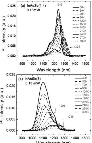
dot densities. The much lower intensity of the ground tran-sition for an Sb BEP of 6⫻10−8 torr reflects a lower dot density. This trend is similar to that observed in the exposed QDs although the reduction is not that strong. Thus, the bur-ied layer has a weaker Sb surfactant effect than the exposed layer, consistent with a weaker Sb incorporation, as shown by the SIMS profile. For low Sb 共BEP=1.4⫻10−8 and 1.8 ⫻10−8 torr兲, as the excitation power increases, the first-excited transition gains increasing relevance and eventually dominates the ground transition; this change is accompanied by the emergence of the second-excited transition. These fea-tures are typically observed in one predominant QD family. Thus, the QDs for low Sb BEP are rather homogeneous. However, for a high Sb BEP of 6⫻10−8 torr, although a typical QD doublet feature is observed at high temperature, the spectra at low temperature differ markedly.
Figures 6共a兲 and 6共b兲 compare the temperature-dependent PL spectra of Sb BEPs of 1.4⫻10−8 and 6 ⫻10−8 torr. As temperature is lowered, the PL spectra for a high Sb BEP of 6⫻10−8 torr show anomalous temperature dependence. The first-excited transition exhibits an abnor-mally large blueshift of 94 meV共from 300 to 30 K兲 versus a blueshift of⬃40 meV for a low Sb BEP of 1.4⫻10−8 torr.
This abnormally large blueshift is accompanied by an enor-mous intensity enhancement and linewidth broadening, caus-ing the PL spectra to be dominated by the enormous peak centered at 1100 nm. The integrated intensity of this peak is more than three times higher than that of the ground transi-tion for Sb BEP of 1.4⫻10−8 torr. This anomalous feature cannot be explained simply by the very wide size dispersion of the QDs. A high-lying energy level with a considerable density must be present to explain the enormously broad 1100 nm peak. This energy level is attributed to a QW-like level, as suggested by the cross-sectional TEM picture in Fig.7. For a low Sb of 1.4⫻10−8 torr, separated QDs with a mean height of 25 nm can be clearly seen. Increasing the Sb BEP to 6⫻10−8 torr substantially reduces the height of the QDs and increases their lateral dimension, causing clustering of the QDs into an undulated QW-like layer with a thickness of 12–15 nm. The reduction in the height of the QDs ex-plains the observed blueshift of the ⬃1300 nm emission as Sb BEP is increased. Notably, the TEM picture shows that the bottom interface of the QW-like layer is relatively flat in comparison with the undulated upper interface. Hence, the clustering mainly occurs in the base of the QDs and the top of the QDs has not yet emerged together. The structure is similar to QDs on a wetting layer with an effective thickness being much thicker than a typical wetting layer for Sb-free QDs but thinner than the height of the QDs. Hence, the emis-sion wavelength from the QW-like layer is expected to be longer than that ⬃900 nm from a typical wetting layer for Sb-free QDs but shorter than the ground transition 共⬃1300 nm兲 of the QDs. This is more or less consistent with the observed anomalous peak centered at 1100 nm. The large broadness of this peak is indicative of the undulated interface of the QW-like layer. At high temperatures, most of the car-riers are confined in the QDs and the PL spectra are domi-nated by their emissions. As temperature is lowered, carriers begin to fill in the QW-like level, and thus the related emis-sion gains increasing relevance, leading to the QW-like PL spectra at low temperature. The formation of this QW-like layer further confirms an Sb surfactant effect that governs the growth of the buried QDs. Both the exposed and buried lay-ers exhibit Sb surfactant effect: A reduction in dot density and a blueshift of PL emission with increasing Sb BEP, and for a high Sb concentration, the exposed layer yields surface
FIG. 6. Temperature-dependent PL spectra for Sb BEP of共a兲 1.4⫻10−8and
共b兲 6⫻10−8 torr. While typical ground-transition dominated PL spectra are
observed for BEP of 1.4⫻10−8 torr, the PL spectra for Sb BEP of 6
⫻10−8 torr display an enormously broad high-energy transition at low
tem-perature, which is attributed to an emission from a QW-like layer due to clustering of the QDs.
FIG. 7. Cross-sectional TEM image of the QDs for Sb BEPs of 1.4⫻10−8
and 6⫻10−8 torr. Separated QDs with mean height of 25 nm are formed for
an Sb BEP of 1.4⫻10−8 torr, while the QDs for Sb BEP of 6⫻10−8 torr
cluster into an undulated QW-like layer with a thickness of 12–15 nm.
023509-4 Chen et al. J. Appl. Phys. 104, 023509共2008兲
IV. CONCLUSIONS
In summary, Sb incorporation into the InAs QDs is shown to modify the density, shape, and PL spectra of the QDs by the Sb surfactant effect. The density of the exposed QDs can be reduced by more than two orders of magnitude by Sb incorporation. This decrease in density is accompanied by a reduction in the height of the QDs and a related PL blueshift. The exposed QDs exhibit a long emission wave-length of ⬃1600 nm with good emission efficiency at 300 K, suggesting that the Sb concentration at the surface can probably reduce the surface recombination velocity of the QDs. However, as the Sb BEP is further increased, the sur-face morphology yields a regular periodic structure of ellip-soid terraces and the buried QDs are simultaneously clus-tered into an undulated 2D layer, giving rise to anomalous QW-like emission at low temperature. These results indicate a marked Sb surfactant effect to suppress the growth of the QDs.
ACKNOWLEDGMENTS
The authors would like to thank the National Science Council of Taiwan共Contract No. NSC-94-2112-M-009-029兲 and the Ministry of Education under the ATU program for financially supporting this research. Dr. R. S. Hsiao is appre-ciated for sample fabrication.
8C. W. Snyder, J. F. Mansfield, and B. G. Orr, Phys. Rev. B46, 9551
共1992兲.
9D. Leonard, M. Krishnamurthy, C. M. Reaves, S. P. Denbaars, and P. M.
Petroff,Appl. Phys. Lett.63, 3203共1993兲.
10H. Shoji, K. Mukai, N. Ohtsuka, M. Sugawara, T. Uchida, and H.
Ish-ikawa,IEEE Photon. Technol. Lett.7, 1385共1995兲.
11H. Saito, K. Nishi, and S. Sugou,Appl. Phys. Lett.73, 2742共1998兲. 12T. Matsuura, T. Miyamoto, T. Kageyama, M. Ohta, Y. Matsui, T. Furuhata,
and F. Koyama,Jpn. J. Appl. Phys., Part 243, L82共2003兲.
13J. M. Ripalda, D. Granados, Y. Gonzalez, A. M. Sanchez, S. I. Molina, and
J. M. Garcia,Appl. Phys. Lett.87, 202108共2005兲.
14H. Y. Liu, M. J. Steer, T. J. Badcock, D. J. Mowbray, M. S. Skolnick, F.
Suarez, J. S. Ng, M. Hopkinson, and J. P. R. David,J. Appl. Phys.99,
046104共2006兲.
15T. Kageyama, T. Miyamoto, M. Ohta, T. Matsuura, Y. Matsui, T. Furuhata,
and F. Koyama,J. Appl. Phys.96, 44共2004兲.
16J. C. Harmand, L. H. Li, G. Patriarche, and L. Travers,Appl. Phys. Lett. 84, 3981共2004兲.
17X. Yang, M. J. Jurlovic, J. B. Heroux, and W. I. Wang,Appl. Phys. Lett. 75, 178共1999兲.
18H. Shimizu, K. Kumada, S. Uchiyama, and A. Kasukawa,Electron. Lett. 36, 1379共2000兲.
19A. Krier, X. L. Huang, and A. Hammiche, Appl. Phys. Lett.77, 3791
共2000兲.
20K. Suzuki and Y. Arakwa,Phys. Status Solidi B224, 139共2001兲. 21T. Matsuura, T. Miyamoto, T. Kageyama, M. Ohta, Y. Matsui, T. Furuhata,
and F. Koyama,Jpn. J. Appl. Phys., Part 243, L605共2004兲.
22J. F. Chen, R. S. Hsiao, W. D. Huang, Y. H. Wu, L. Chang, J. S. Wang, and
J. Y. Chi,Appl. Phys. Lett.88, 233113共2006兲.
23Y. Sun, S. F. Cheng, G. Chen, R. F. Hicks, J. G. Cederberg, and R. M.
Biefeld,J. Appl. Phys.97, 053503共2005兲.
24B. N. Zvonkov, I. A. Karpovich, N. V. Baidus, D. O. Filatov, S. V.
Moro-zov, and Y. Y. Gushina,Nanotechnology11, 221共2000兲. 25Y. P. Varshni,Physica共Amsterdam兲34, 149共1967兲.