Band gap engineering and stimulated emission of ZnMgO nanowires
Hsu-Cheng Hsu, Chun-Yi Wu, Hsin-Ming Cheng, and Wen-Feng Hsieh
Citation: Applied Physics Letters 89, 013101 (2006); doi: 10.1063/1.2218813
View online: http://dx.doi.org/10.1063/1.2218813
View Table of Contents: http://scitation.aip.org/content/aip/journal/apl/89/1?ver=pdfcov Published by the AIP Publishing
Articles you may be interested in
An empirical law for the band gaps of MgZnO nanowires J. Appl. Phys. 110, 124315 (2011); 10.1063/1.3671013
Indium-doped ZnO nanowires: Optical properties and room-temperature ferromagnetism J. Appl. Phys. 108, 043516 (2010); 10.1063/1.3464229
Electrical properties and near band edge emission of Bi-doped ZnO nanowires Appl. Phys. Lett. 90, 083113 (2007); 10.1063/1.2431715
Determination of carrier density of ZnO nanowires by electrochemical techniques Appl. Phys. Lett. 89, 203117 (2006); 10.1063/1.2390667
Blueshift of near band edge emission in Mg doped ZnO thin films and aging J. Appl. Phys. 95, 4772 (2004); 10.1063/1.1690091
This article is copyrighted as indicated in the article. Reuse of AIP content is subject to the terms at: http://scitation.aip.org/termsconditions. Downloaded to IP: 140.113.38.11 On: Thu, 01 May 2014 01:54:45
Band gap engineering and stimulated emission of ZnMgO nanowires
Hsu-Cheng Hsu, Chun-Yi Wu, Hsin-Ming Cheng,a兲 and Wen-Feng Hsiehb兲
Department of Photonics and Institute of Electro-Optical Engineering, National Chiao Tung University, Hsinchu 300, Taiwan
共Received 26 January 2006; accepted 29 May 2006; published online 5 July 2006兲
We report a simple method for fabricating heterostructured ZnMgO nanowires by annealing the preformed ZnO / MgO core-shell structure. Photoluminescence from the alloy nanowires shows strong near-band-edge 共NBE兲 emission, reflecting good material quality. A blueshift of the NBE emission at room temperature after the annealing treatment is attributed to the diffusion of Mg from the shell into the core ZnO of the nanowires to form a ternary ZnMgO alloy. Band gap engineering and stimulated emissions of ZnMgO nanowires with different Mg doping concentrations are also demonstrated. © 2006 American Institute of Physics.关DOI:10.1063/1.2218813兴
One-dimensional nanostructures have attracted a great deal of attention for their special properties and applications in microsensing for chemical-biological agent detection, so-lar energy conversion, solid-state lighting, and the like.1–5 ZnO, with a wide gap of 3.37 eV and a large exciton binding energy of 60 meV, has been recognized as a key photonic material in the blue-UV region.6,7The greatest challenges in realizing photonic devices based on ZnO nanowires are het-erostructure, p-type doping, and band gap engineering. In practical applications, the ability to fabricate a laser of a predetermined wavelength is critical.
Alloying the ZnO phase with MgO and ZnS has been investigated for widening the band gap of ZnO-based nanowires.8–14A blueshift of the UV emission with respect to that of the pure ZnO nanowires has been observed while the ZnO nanowires were doped with sulfur.10,11 The room-temperature photoluminescence12and absorption spectra13of the ZnMgO nanowires were tuned by adjusting the Mg con-centration. However, there are no reported studies on stimu-lated emissions共SEs兲 from ZnMgO alloy nanowires at room temperature. In this letter, we demonstrate a simple method to achieve the band gap engineering in ZnO / MgO core-shell nanowires by using Mg diffusion. While the annealing tem-perature increases, the diffused concentration of Mg in-creases, which results in a blueshift of PL UV-emission spec-tra at room temperature. Furthermore, we report the observation of optically pumped stimulated emissions from the ZnMgO nanowires.
Synthesis of ZnMgO nanostructures was carried out in a simple vapor transport process. A mixture of zinc powder 共99.9999%兲 and magnesium powder 共99.6%兲 with Mg:Zn weight ratios of 1:19 was placed in a ceramic boat as the starting materials and an a-plane sapphire wafer was used as a substrate. The boat was positioned in the center of the quartz furnace tube and the substrate was placed 10 mm downstream from the mixed powders. Before heating the fur-nace, the quartz tube was purged twice with high-purity ar-gon gas for 3 min periods. The system was then heated to 570 ° C共at a heating rate of 50 °C/min兲 with an Ar flow rate of 500 SCCM共SCCM denotes cubic centimeter per minute
at STP兲 and was kept at this temperature for 60 min. At the end of the process the products were treated under ambient atmospheric pressure for 120 min at temperatures ranging from 800 to 1000 ° C.
The morphology, composition, and crystallinity of the products were characterized through the use of scanning electron microscopy共SEM兲, energy dispersive x-ray 共EDX兲, x-ray diffraction 共XRD兲, and transmission electron micros-copy 共TEM兲. For the continuous-wave 共cw兲 PL measure-ment, we used a He–Cd laser 共3.81 eV兲 as the excitation source, while for the stimulated emission measurement, we used the third harmonic of a pulsed-pumped Nd: YVO4 共yt-trium vanadate兲 laser 共3.51 eV兲 with a pulse width of ⬃500 ps and a repetition rate of 1 kHz.15
The emission light was dispersed in a 32 cm monochromator and detected by an UV-sensitive photomultiplier tube.
Figure 1共a兲 shows the SEM images of the as-grown products. All the products are nanowires with a diameter of 200– 500 nm and a length of over 5m. Figure 1共b兲 shows the EDX pattern of the as-grown nanowires, which are com-posed mainly of Mg and O with a small amount of Zn. The typical XRD pattern of the nanowires is shown in Fig. 1共c兲. All sharp diffraction peaks can be perfectly indexed to a high crystallinity in the hexagonal structure of ZnO and the face-centered-cubic structure of MgO. The TEM image of the as-grown nanowires in Fig. 2共a兲 shows that an individual nanowire displays good contrast, distinguishing the core and sheath regions. The core has a diameter of about 90 nm and is capped with a sheath about 200 nm thick. The EDX pat-tern in Fig. 2共b兲 indicates that the nanowire is composed of Mg and O with a small amount of Zn. The high resolution TEM共HRTEM兲 image in Fig. 2共c兲, which is taken from the edge共sheath region兲 of the nanowire, shows a perfect lattice plane with an interplanar spacing of 2.1 nm, which is in good agreement with the 共002兲 spacing of MgO. The selection-area electron diffraction 共SAED兲 pattern of this region 关see Fig. 2共d兲兴 shows that the outer layer of the nanowires is single-crystalline MgO with a cubic rocksalt structure. Based on these observations, we proposed that the nanowires should be formed of a ZnO / MgO core-shell heterostructure as illustrated in Fig. 2共e兲.
The growth of the ZnO / MgO core-shell nanowires dis-cussed above was accomplished by simple thermal evapora-tion of Zn and Mg powders. The proposed growth process follows: Because the melting point of Zn 共⬃419 °C兲 is
a兲Also at: Material and Chemical Research Laboratories, Industrial
Technol-ogy Research Institute, Hsinchu 310, Taiwan.
b兲Author to whom correspondence should be addressed; electronic mail:
wfhsieh@mail.nctu.edu.tw
APPLIED PHYSICS LETTERS 89, 013101共2006兲
0003-6951/2006/89共1兲/013101/3/$23.00 89, 013101-1 © 2006 American Institute of Physics
This article is copyrighted as indicated in the article. Reuse of AIP content is subject to the terms at: http://scitation.aip.org/termsconditions. Downloaded to IP: 140.113.38.11 On: Thu, 01 May 2014 01:54:45
lower than that of Mg 共650 °C兲, the Zn powder would evaporate before the Mg powder does as the processing tem-perature increases. In the present case, because no evidence for catalyst particles can be observed on any tip of the syn-thesized nanowires, the vapor-solid共VS兲 mechanism would be a reasonable explanation for the growth of the core ZnO
nanowires. The follow-up vaporization of Mg would con-dense on the ZnO nanowires and be oxidized rapidly to form the MgO sheath structure and to lead to the formation of the ZnO / MgO core-shell nanowires.
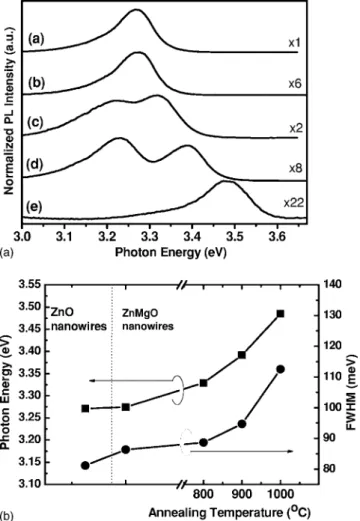
Figure 3共a兲 shows the room-temperature PL spectra of the ZnO / MgO core-shell nanowires annealed at tempera-tures ranging from 800 to 1000 ° C. The PL of the pure ZnO is also shown in Fig. 3共a兲 as a reference. For the undoped ZnO nanowires and the as-grown ZnO / MgO core-shell nanowires, a near-band-edge 共NBE兲 emission peak of 3.27 eV with the full width at half maximum 共FWHM兲 of ⬃85 meV is the result of the free exciton emission.16–18
As shown in Fig. 3共b兲, the excitonic transition energy and line-width increase as a function of the annealing temperature. Meanwhile, another peak appears at 3.23 eV on the low-energy side of the excitonic band. The origin of the emission peak should be attributed to the free exciton emission of the residual inner core of the nondiffused ZnO nanowires. When the thermal treatment temperature reaches 1100 ° C, the peak at 3.23 eV vanishes, indicating that the interdiffusion process is completely finished. The dramatically blueshifted emission can be attributed to the increase in Mg composition in the ternary ZnMgO through interdiffusion. The broadening of the main peak reflects the increase in fluctuation of the com-position and lattice disorder in the alloy. A decrease of the PL intensity with increasing Mg concentration results from the FIG. 1. 共a兲 Typical SEM image 共b兲 EDX pattern, and 共c兲 XRD of the
as-grown nanowires.
FIG. 2.共Color online兲 共a兲 TEM image of the as-grown nanowires; 共b兲 EDX analysis showing the nanowire is composed of Zn, Mg, and O;共c兲 HRTEM image showing the edge of the nanowire;共d兲 SAED at the edge of the nanowire showing single-crystalline cubic rocksalt structure;共d兲 schematic model of the core-shell nanowire.
FIG. 3.共a兲 Room-temperature PL spectra of 共a兲 pure ZnO nanowires and 共b兲 the as-grown ZnO / MgO core-shell nanowires annealed at different tempera-tures ranging from共c兲 800, 共d兲 900, and 共e兲 1000 °C. 共b兲 shows the peak energy of excitonic emission of ZnO / MgO core-shell nanowires and the corresponding FWHM as a function of annealing temperature.
013101-2 Hsu et al. Appl. Phys. Lett. 89, 013101共2006兲
This article is copyrighted as indicated in the article. Reuse of AIP content is subject to the terms at: http://scitation.aip.org/termsconditions. Downloaded to IP: 140.113.38.11 On: Thu, 01 May 2014 01:54:45
increase in nonradiative recombination processes.
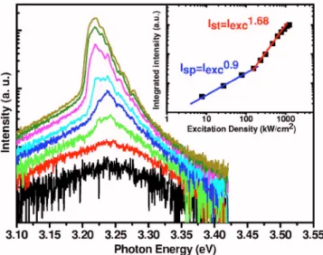
Figure 4 shows a semilog plot of the typical NBE spec-trum and the corresponding peak intensity as a function of excitation density共Iexc兲 under pulsed pumping for the sample annealed at 800 ° C. At low excitation densities, only a broad spontaneous emission peak can be observed at 3.25 eV with the FWHM of⬃0.1 eV. As shown in the inset in Fig. 4, the emission intensity was found to be approximately linearly proportional to the excitation power density, indicating that the broad emission is typical spontaneous emission. As the excitation pump density increases to a value exceeding a threshold of about 200 kW/ cm2, a spectrally narrower peak with the FWHM of 24 meV appears at the top of the low-energy shoulder of the spontaneous emission. The emission intensity of this narrower feature becomes dominant as the pumping power density is increased to above the threshold. The strong, narrow emission exhibits a superlinear increase, indicating the appearance of SE. The SE is attributed to the stimulated recombination of exciton-exciton scattering,19,20 which is a two-particle process; therefore, a dependence of
Iexc as ISE⬀Iexc␣ , with␣⬃2, can be expected. Our analysis shows a value of ␣= 2.08 for the as-grown sample and ␣ = 1.68 and␣= 1.45 for the samples with annealed tempera-tures of 800 and 900 ° C, respectively. As expected, the ex-ponent␣ is 2.08 for the as-grown samples; however, it de-creases to 1.45 for the 900 ° C-annealed sample. This result indicates that the material quality degrades after the Mg dif-fusion process, owing to the additional scattering centers in-troduced by impurities and defects. Many nonradiative cen-ters or other loss mechanisms formed after more diffusion of the Mg and caused a reduction in the cross section共or
prob-ability兲 of exciton-exciton scattering. Thus, the efficiency of the stimulated emission decreased.
In conclusion, we have synthesized heterostructured Zn-MgO alloy nanowires by a simple evaporation route. The formation of the ZnO / MgO core-shell structure is based on the melting point of Zn being lower than that of Mg. After the annealing treatment, a blueshift in the near-band-edge emission at room temperature is attributed to Mg diffusion into the core ZnO nanowires to form a ternary ZnMgO alloy. Band gap engineering and stimulated emission of ZnMgO nanowires with different Mg doping concentrations are also achieved. This demonstration of the stimulated emission at room temperature from MgZnO nanowires could be used for light-emitting device applications.
This work is supported by the National Science Council 共NSC兲 of the Republic of China under Grant No. 94-2112-M009-015. The authors thank the Nano Technology Re-search Center of ITRI for electron microscopy measurements.
1J. Hahm and C. M. Lieber, Nano Lett. 4, 51共2004兲.
2H. Kind, H. Q. Yan, B. Messer, M. Law, and P. D. Yang, Adv. Mater.
共Weinheim, Ger.兲 14, 158 共2002兲.
3M. Law, L. E. Greene, J. C. Johnson, R. Saykally, and P. D. Yang, Nat.
Mater. 4, 455共2005兲.
4Y. N. Xia, P. D. Yang, Y. G. Sun, Y. Y. Wu, B. Mayers, B. Gates, Y. D.
Yin, F. Kim, and Y. Q. Yan, Adv. Mater.共Weinheim, Ger.兲 15, 353 共2003兲.
5S. Gradecak, F. Qian, Y. Li, H. G. Park, and C. M. Lieber, Appl. Phys.
Lett. 87, 173111共2005兲.
6D. C. Look, Mater. Sci. Eng., B 80, 383共2001兲.
7U. Ozgur, Y. T. Alivov, C. Liu, A. Teke, M. A. Reshchikov, S. Dogan, V.
Avrutin, S. J. Cho, and H. Morkoc, J. Appl. Phys. 98, 041301共2005兲.
8Y. W. Heo, M. Kaufman, K. Pruessner, D. P. Norton, F. Ren, M. F.
Chisholm, and P. H. Fleming, Solid-State Electron. 47, 2269共2003兲.
9Y. W. Heo, C. Abernathy, K. Pruessner, W. Sigmund, D. P. Norton, M.
Overberg, F. Ren, and M. F. Chisholm, J. Appl. Phys. 96, 6共2004兲.
10B. Y. Geng, G. Z. Wang, Z. Jiang, T. Xie, S. H. Sun, G. W. Meng, and L.
D. Zhang, Appl. Phys. Lett. 82, 4791共2003兲.
11G. Shen, J. H. Cho, J. K. Yoo, G. C. Yi, and C. J. Lee, J. Phys. Chem. B 109, 5491共2005兲.
12C. H. Ku, H. H. Chiang, and J. J. Wu, Chem. Phys. Lett. 404, 132共2005兲. 13C. Y. Lee, T. Y. Tseng, S. Y. Li, and P. Lin, Nanotechnology 16, 1105
共2005兲.
14M. Lorenz, E. M. Kaidashev, A. Rahm, Th. Nobis, J. Lenzner, G. Wagner,
D. Spemann, H. Hochmuth, and M. Grundmann, Appl. Phys. Lett. 86, 043113共2005兲.
15H. C. Hsu, C. Y. Wu, and W. F. Hsieh, J. Appl. Phys. 97, 064315共2005兲. 16H. C. Hsu, Y. K. Tseng, H. M. Chang, J. H. Kuo, and W. F. Hsieh, J. Cryst.
Growth 261, 520共2004兲.
17B. P. Zhang, N. T. Binh, Y. Segawa, Y. Kashiwaba, and K. Haga, Appl.
Phys. Lett. 84, 586共2004兲.
18H. C. Hsu, C. S. Cheng, C. C. Chang, S. Yang, C. S. Chang, and W. F.
Hsieh, Nanotechnology 16, 297共2005兲.
19D. M. Bagnall, Y. F. Chen, Z. Zhu, T. Yao, S. Koyama, M. Y. Shen, and T.
Goto, Appl. Phys. Lett. 70, 2230共1997兲.
20Y. F. Chen, N. T. Tuan, Y. Segawa, H. J. Ko, S. K. Hong, and T. Yao,
Appl. Phys. Lett. 78, 1469共2001兲. FIG. 4.共Color online兲 The RT emission spectra as a function of excitation
intensity for 800 ° C-annealed ZnO / MgO core-shell nanowires. The inset shows its log-log plots of integrated emission intensity vs the excitation intensity.
013101-3 Hsu et al. Appl. Phys. Lett. 89, 013101共2006兲
This article is copyrighted as indicated in the article. Reuse of AIP content is subject to the terms at: http://scitation.aip.org/termsconditions. Downloaded to IP: 140.113.38.11 On: Thu, 01 May 2014 01:54:45