Morphology and Contact Angle Characterization of Deposited PE-PEO Diblock Copolymer on Silicon wafer
4
0
0
全文
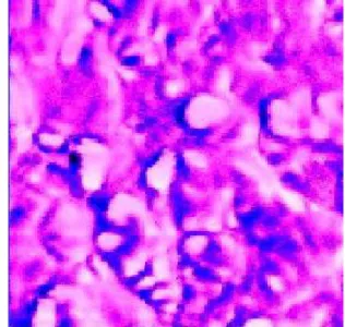
(2) angle shows the potential to forma an amphiphobic surface. Fig. 3 shows the surface morphology of a pure silicon wafer. The scan size is 500 nm by 500 nm. The local surface roughness is calculated by AFM as Rq = 0.10 nm, indicating that the surface is very smooth with a sub-nm roughness and that the calculated roughness has fallen within the hardware noise range. In addition, In addition, the contact angles show the surface is hydrophobic as expected. Fig. 4 shows the AFM image of the thermally treated silicon wafer surface. The scan size is 500 nm by 500 nm. The thickness of the oxide layer is estimated to be about 148 nm from the depths of the pinholes. After thermal oxidation, the surface became more hydrophilic with the water contact angle decreasing from 55˚ to 45˚ (Fig. 1). The root-mean-square surface roughness Rq increased from 0.10 nm to 0.74 nm, indicating the formation of silica oxide. The pinholes may result from the chip-off defects due to expansion of the silicon surface layer on oxidation. After thermal oxidation, the silicon layer was modified by OTMS. The water contact angle jumped up to 130˚ due to the hydrophobic tails of silane (Fig. 1). The coupling agent underwent the sol-gel reactions with the oxide layer of silicon to form the Si-O-Si covalent bonds. After washing the silane layer with solvent for a few times, the surface hydrophobicity still retained, indicating the success of modification. Although the hydrophobicity increased a lot, it did not increase the lyophilicity accordingly. The oil contact angle did not decrease after the surface modification. Surface nano-structures, exposed oxide layer, or scattered fine particles of silica gel from silane might contribute to this phenomenon. Fig. 5 shows the AFM image of the silane layer over the oxide layer. The scan size is 500 nm by 500 nm. The morphology is quite different from that of Fig. 4 to the naked eye. Further, the surface roughness Rq increased again from 0.74 nm to 1.2 nm, implying a relatively high surface coverage by the silane agent. The oxide pinholes are not as dense in number as observed in Fig. 4, indicating the filling up by silane. Fig. 6 shows the AFM image of the annealed PE-PEO layer over the silane layer. The scan size is 500 nm by 500 nm. Morphology of netted polymer films with pinholes could be observed. However, the outlook of the pinholes in this layer is quite different from that in the silicon oxide layer. The local surface roughness Rq has increased to 5.7 nm, indicating a relatively rough surface. Contact angle data show that the hydrophobicity drops a little bit while the lyophobicity keeps increasing (Fig. 1). On annealing the film, the PE segments of the PE-PEO copolymer are expected to move and entangle with the alkyl tails of the silane layer. Such a thermal fusion should be able to push the more hydrophilic PEO segments to the surface of the coating, thus to lower the surface hydrophobicity, which explains the change in water contact angle. In Fig. 7, the AFM phase image reveals the micro-phase separation of the PE-PEO diblock copolymer after annealing. The scan size is 500 nm by 500 nm. The different color shades in the image normally refer to different components in the sample as well as the regions of large slope. Fig. 7 gives a striated pattern which might denote domains of PE, PEO, and silica. Hence, the surface wettability is determined by all the materials exposed on the surface. The PEO blocks might take the form of hydrophilic islands on the surface. By improving and utilizing such self-assembled micro/nano-structures, a better surface amphiphobicity is expected and currently being sought in our lab.. In the future, the concentrations and relative lengths of the two blocks in PE-PEO and the temperatures of thermal oxidation and annealing will be studied to understand their effects on the self-assembled patterns and amphiphobicity. Further, a similar process will be applied to real textile to study the effects of the surface modification. 4. List of Figures CH3CH2(CH2CH2)x-(OCH2CH2)yOH Fig. 1. Chemical structure of PE-PEO. Fig. 2. Plot of contact angles of oil and water against treated silicon wafer surfaces. Wafer 1 is thermally oxidized; wafer 2 is thermally oxidized and then coated with the silane coupling agent; wafer 3 comprises PE-PEO diblock copolymer spin-coated on wafer 2 and annealed. The scan size is 500 nm by 500 nm.. Fig. 3. AFM image of bare silicon wafer surface. The scan size is 500 nm by 500 nm..
(3) Fig. 6. AFM image of PE-PEO layer deposited and annealed on the silanol/oxide/silicon wafer surface. The scan size is 500 nm by 500 nm.. Fig. 4. AFM image of thermally oxidized silicon wafer surface. The scan size is 500 nm by 500 nm. Fig. 7. AFM phase image of PE-PEO layer deposited on the silanol/oxide/silicon wafer surface. The scan size is 500 nm by 500 nm. 5. Conclusions. Fig. 5. AFM image of silicon oxide surface modified by alkoxyl silane coupling agent. The scan size is 500 nm by 500 nm.. Micro/nano-patterns of the diblock copolymer, PE-PEO, have been created to change and adjust the surface properties of a silicon wafer. Results show that the surface of pure silicon renders hydrophilic after thermal oxidation. Further treatment with alkoxyl silane coupling agent, the water contact angle becomes 130˚ and the oil one, 28˚. The slow increase in oil contact angle shows potential in creating amphiphobic surface coatings. The root-mean-square roughness, Rq, increases from sub-nanometer to 1.2 nm calculated using AFM, indicating a high surface coverage of the coupling agent over the silica layer and the formation of covalent bonds. In addition, due to the thermal induced entangling of the PE blocks and the alkyl tails of silane, the hydrophilic PEO blocks could be moved to the top of the coating, rendering a more hydrophilic surface while holding down the oil contact angle. Self-assembled striated patterns indicating mixed but separated hydrophilic and hydrophobic regions have been found for the PE-PEO diblock copolymer coatings in the phase images of AFM. Acknowledgements This research was supported in part by National Science Council, Taiwan, under Contract 94-2622-E-035-007-CC3 References [1]. [2]. [3]. E. Buck and J. Fuhrmann, “Surface-Induced Microphase Separation in Spin-Cast Ultrathin Diblock Copolymer Films on Silicon Substrate before and after Annealing” Macromolecules 2001, 34, 2172-2178 Z. Lu, G. Liu, F. Liu, “Block Copolymer Microspheres Containing Intricate Nanometer-Sized Segregation Patterns” Macromolecules 2001, 34, 8814-8817 A. Adedeji, S. Lyu, C. W. Macosko, “Block Copolymers in Homopolymer Blends: Interface vs Micelles”.
(4) [4]. [5]. Macromolecules 2001, 34, 8663-8668 G. Zhang, N. Fu, H. Zhang, J. Wang, X. Hou, B. Yang, J. Shen, Y. Li, and L. Jiang, “Controlling Pore Size and Wettability of a Unique Microheterogeneous Copolymer Film with Porous Structure” Langmuir 2003, 19, 2434-2443 Y. Deng, J. B. Dixon, G. N. White, “Bonding mechanisms and conformation of poly(ethylene oxide)-based surfactants in interlayer of smectite” Colloid Polym. Sci. (2006) 284: 347–356.
(5)
數據
相關文件
Wet chemical etchings are especially suitable for blanket etches (i.e., over the whole wafer surface) of polysilicon, oxide, nitride, metals, and Ⅲ-Ⅴ compounds. The
These kind of defects will escape from a high temperature wafer sort test and then suffer FT yield, so it is necessary to add an extra cold temperature CP test in order to improve
The bottleneck stations with multiple machines are generally in the industry, such as semiconductor wafer manufacturing plants, IC substrate manufacturing plants,
The second coated layer is the Ag reference mirror layer with the thickness of about 100nm, 450nm and 900nm corresponding to sapphire/Ti/Ag/AuSn, sapphire/Cr/Ag/AuSn, and
hands sensory contact with the soil medium high repellency.3 、 In accordance with Based on Welfare benefits Pretest and posttest Checklist of
我們是以瑕疵圖 ( Defect Map ) 來分析多方塊,首先由原有的一 片晶圓圖 ( Wafer Map ) 經過瑕疵數 ( Defect Number )
This thesis is mainly from numerous semiconductor industry's companies and academic organizations,Investigate and is it have something to do with wafer and wafer fabrication
Capacity determination model with time constraints and batch processing in semiconductor wafer fabrication.. Approximations For The
