國
立
交
通
大
學
材料科學與工程學系
碩
士
論
文
金屬/半導體核殼奈米晶體之光催化特性研究
Investigation on Photocatalytic Properties of Metal/Semiconductor
Core/Shell Nanocrystals
研 究 生:楊婷婷
指導教授:徐雍鎣 教授
中 華 民 國 一 百 零 一 年 九 月
金屬/半導體核殼奈米晶體之光催化特性研究
Investigation on Photocatalytic Properties of Metal/Semiconductor
Core/Shell Nanocrystals
研 究 生:楊婷婷 Student:Ting-Ting Yang
指導教授:徐雍鎣
Advisor:Yung-Jung Hsu
國 立 交 通 大 學
材 料 科 學 與 工 程 學 系
碩 士 論 文
A ThesisSubmitted to Department of Materials Science and Engineering College of Engineering
National Chiao Tung University in partial Fulfillment of the Requirements
for the Degree of Master
in
Materials Science and Engineering
September 2012
Hsinchu, Taiwan, Republic of China
中華民國一百零一年九月
金 屬 / 半 導 體 核 殼 奈 米 晶 體 之 光 催 化 特 性 研 究
學生:楊婷婷
指導教授:徐雍鎣
××××× ×××××國立交通大學材料科學與工程學系碩士班
摘
要
本研究論文之主要成果乃在於開發出一新穎製程,以獲得具有均勻殼層包覆
之 Au-CdS 核殼奈米晶體,經由合成條件的改變,其殼層的厚度可被精確地調控。
Au-CdS 核殼晶體乃被證實具有光誘發載子分離之效果,此一現象源自於 Au 與
CdS 之相對能帶結構所致,經照光後於 CdS 殼層內被激發之電子,可藉由 Au-CdS
異質介面的存在而轉移至 Au 端,並且留下大量電洞於 CdS 殼層內。藉由載子傳
輸動力學的量測,此發生於 Au-CdS 核殼奈米晶體內之載子分離現象,可有效被
定量化描述與討論,量測結果顯示電子經由 CdS 傳輸至 Au 端之速率常數,隨著
殼層厚度的增加而上升。由於此 Au-CdS 核殼奈米晶體在光照後具有良好的載子
分離效果,故當其進一步被運用於光催化反應系統中時,也展現出相當優異之催
化效能;其中,CdS 殼層越厚之 Au-CdS 奈米晶體其光催化效果越佳,此現象與
電子傳輸速率常數變化的趨勢相符。在可見光的照射下,此 Au-CdS 核殼奈米晶
體的光催化效能也優於 N-doped P-25 TiO
2和 CdS 塊材粉末之商用品,使其相當
有潛力成為具高效光催化能力之可見光觸媒。此外,為提昇其耐久性以利長時間
之應用,吾人在製備過程中加入 Zn,以形成 Au-Cd
1-xZn
xS 核殼奈米晶體。在重
複使用於光催化的過程中,Au-Cd
1-xZn
xS 核殼奈米晶體展現了更佳的穩定性。由
本研究所開發之製程亦可延伸應用於以其它硫化物做為殼層的金-半導體核殼奈
米晶體之合成,例如 Au-ZnS,且可將其應用於光電化學電池中甲醇氧化反應之
催化。
附件五 橫式中文摘要格式樣本Investigation on Photocatalytic Properties of Metal/Semiconductor
Core/Shell Nanocrystals
student:Ting-Ting Yang
Advisors:Dr. Yung-Jung Hsu
Dr.
------Dr.
-----Department of Materials Science and Engineering
National Chiao Tung University
ABSTRACT
A facile and reproducible synthetic approach for preparation of core-shell Au-CdS
nanocrystals with controllable shell thickness was reported. Due to the difference in
band structures between Au and CdS, a pronounced photoinduced charge separation
took place at the interface of Au and CdS, resulting in the electron-charged Au core
and the hole-enriched CdS shell. The electron-charging of Au core in Au-CdS
nanocrystals was revealed with the charge carrier dynamics measurement. An increase
in the electron-transfer rate constant was observed for Au-CdS nanocrystals with
increasing shell thickness, probably due to the less pronounced electron-hole
interaction of thicker CdS that enabled a fuller extent of participation of photoexcited
electrons in the charge separation process. On the other hand, the hole-enriched CdS
shell of Au-CdS nanocrystals upon light illumination was characterized with a
photocatalytic process. The photocatalytic activity of Au-CdS nanocrystals was found
to increase with increasing shell thickness, attributable to the greater capability of
light absorption achieved by the extensive growth of the CdS shell. The correlation of
photocatalytic activity with the shell thickness of Au-CdS nanocrystals corresponded
well with that of the electron-transfer rate constant. As compared to the relevant
commercial products like N-doped P-25 TiO
2and CdS powders, the as-synthesized
Au-CdS nanocrystals exhibited superior photocatalytic performance under visible
light illumination, demonstrating their potential as an effective visible-light-driven
photocatalyst. To further enhance the durability performance, Zn was introduced into
the shell of Au-CdS, producing Au-Cd
1-xZn
xS nanocrystals that showed relatively high
stability in photocatalysis. The present synthetic route can be readily extended to
obtain other sulfide-semiconductor-coated Au nanocrystals, such as Au-ZnS, which
may find potential use for methanol oxidation in the photoelectrochemical cell.
誌
謝
一轉眼五年就過去了。回想起五年前剛進實驗室的暑假,當時也只是剛要升
大三的小專題生,而我們的實驗室也才剛起步。回想起當初打掃完後實驗室裡空
無一物、等儀器公司來規劃施工實驗桌,碩博班加上專題生總共只有六個人;一
直到現在實驗室裡擺滿了各種儀器及實驗用品,人口眾多做實驗須輪流,一切的
光景真是不可同日而語。非常感謝徐雍鎣老師當初願意收留課業成績很差的我做
為專題生,才讓我能夠成為實驗室元老成員之一,感覺好像在寫下歷史的一部
分。也感謝老師一路以來的指導與幫忙,除了讓我立定志向唸碩士之外,也讓我
有機會到國外增廣見聞。另外,最感謝的當然就是一手包辦實驗室大小事務且一
路帶著我的韋達學長,讓我從一開始什麼都不會到最後能獨立做出一些小小研
究,並且總是不吝與我分享成果,甚至將我列入期刊論文的共同作者,讓我得以
順利推甄上研究所以及獲得出國做實驗的機會。非常感謝實驗室所有成員一路上
的幫忙,特別是總是天南地北的陪我聊天亂跑的宜芳以及總是在緊張時刻鼓勵我
的韋豪,也感謝我的室友們總是讓我有繼續打拚的動力。感謝有新光計畫、胤諴、
玟娟、一餐黑派泥斯老闆夫婦、前廣翰楊先生等等,讓我的研究生活除了實驗之
外有更豐富的色彩,累的時候也能有個休息站。感謝家人不可或缺的支持,這本
論文才得以產生。短短的篇幅及有限的記憶力,一定有許多該感謝的人事物沒有
被寫進這篇致謝,但感謝的心意是不變的。Thanks a lot!
附件七 誌謝格式Table of Contents
摘要 ……… i Abstract ……… ii Acknowledgment ……… iii Table of Contents ……… iv List of Tables ……… v List of Figures ……… viChapter 1 Introduction and Paper Review………. 1
Chapter 2 Motivation and Experiment ……… 7
2-1 Motivation……….. 7
2-2 Experimental Section………. 10
2-2.1 Chemicals……….. 10
2-2.2 Preparation of Au colloids………. 10
2-2.3 Preparation of Au-CdS core-shell Nanocrystals……… 10
2-2.4 Extensive growth of CdS shell……….. 11
2-2.5 Preparation of Au-Cd1-xZnxS Nanocrystals………... 11
2-2.6 Preparation of Au-ZnS Nanocrystals………. 12
2-2.7 Preparation of CdS Counterpart Nanocrystals………... 12
2-2.8 Preparation of N-Doped P-25 TiO2……… 12
2-2.9 Photocurrent Measurement……… 13
2-2.10 Photoluminescence Lifetime Measurement………... 13
2-2.11 Photocatalytic Activity Measurement……… 14
2-2.12 Photoelecrtochemical Catalytic Activity Measurement…… 14
2-2.13 Characterizations……… 15
2-3 Results and discussion……… 16
2-3.1 Au-CdS Core-Shell Nanocrystals……….. 16
2-3.2 Au-CdxZnyS Core–Shell Nanocrystals……….. 38
2-3.3 Au-ZnS Core–Shell Nanocrystals………. 40
Chapter 3 Conclusions and Future Work……… 45
3-1 Conclusions……… 45
3-2 Future Work……… 46
References ……… 47
List of Tables
Table 1. Kinetic analysis of emission decay for Au-CdS nanocrystals with various shell thicknesses and their corresponding CdS counterparts……… 30
List of Figures
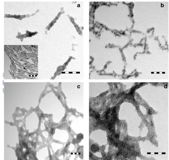
Figure 1. TEM images of hybrid CdSe-Pt samples prepared at different pH values (scale bars: 50 nm). (a) Isolated nanorod structure at pH=10. The inset shows the original rod sample with dimensions of 70 nm × 8 nm. (b) Intermediate structure at pH=7. (c) (d) Nanonet structure at pH=4……….. 2
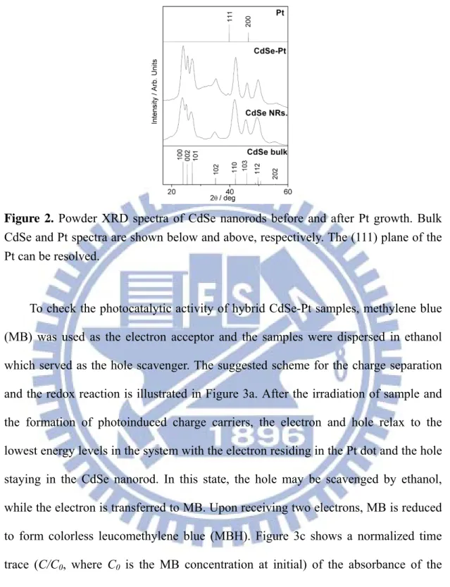
Figure 2. Powder XRD spectra of CdSe nanorods before and after Pt growth. Bulk CdSe and Pt spectra are shown below and above, respectively. The (111) plane of the Pt can be resolved……….. 3
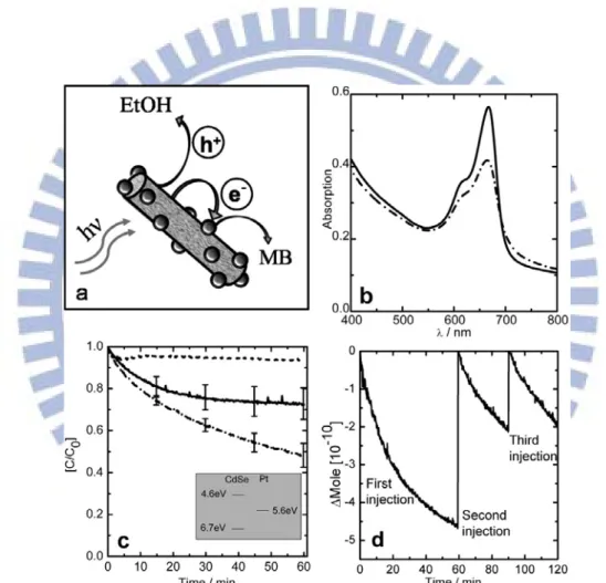
Figure 3. Photocatalysis by using hybrid CdSe-Pt samples. (a) Scheme of the photo-induced charge separation in CdSe-Pt nanorods. (b) Absorbance spectra of MB and CdSe-Pt nanonets mixture before (solid line) and after 60 min of irradiation (dashed-dotted line). (c) Time traces of the normalized concentration of MB for CdSe-Pt nanonets (dashed-dotted line), CdSe-Pt isolated nanorods (solid line) and the physical mixture (dashed line). (d) Recycling photocatalysis experiment for CdSe-Pt nanonets.…… 4
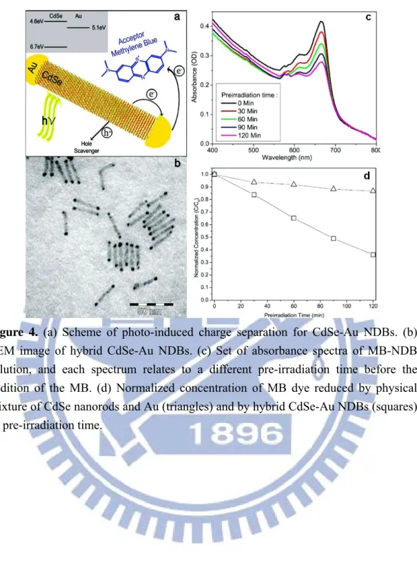
Figure 4. (a) Scheme of photo-induced charge separation for CdSe-Au NDBs. (b) TEM image of hybrid CdSe-Au NDBs. (c) Set of absorbance spectra of MB-NDB solution, and each spectrum relates to a different pre-irradiation time before the addition of the MB. (d) Normalized concentration of MB dye reduced by physical mixture of CdSe nanorods and Au (triangles) and by hybrid CdSe-Au NDBs (squares) vs pre-irradiation time.……… 6
Figure 5. XPS spectra of (a) N1s and (b) C1s peaks for Au-(Cys/Cd) colloids.……….. 16
Figure 6. UV-Visible absorption spectra of Au-Cit and Au-(Cys/Cd) colloids with various Cys:Cd2+ ratios. The concentration of
Cys/Cd is 5 mM.………. 17
Figure 7. XRD pattern of Au-CdS nanocrystals with the reference fcc Au
(JCPDS#04-0784) and wurtzite CdS (JCPDS#06-0314) included
for comparison.……… 19
Figure 8. Au-CdS nanocrystals prepared with a Cys/Cd concentration of 5 mM: (a) low-magnification TEM images; (b) TEM-EDS elemental mapping taken on a single core-shell particle; (c) HRTEM image and (d) the corresponding SAED pattern of a single core-shell particle. The scale bar of the inset in (a) is 20 nm.………. 19
.
Figure 9. XPS spectrum of C1s peak for Au-CdS core-shell nanocrystals.……… 21
Figure 10. Enlarged HRTEM image taken at the interface of Au and CdS regions on a single Au-CdS nanocrystal.………. 21
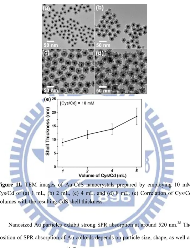
Figure 11. TEM images of Au-CdS nanocrystals prepared by employing 10 mM Cys/Cd of (a) 1 mL, (b) 2 mL, (c) 4 mL, and (d) 8 mL. (e) Correlation of Cys/Cd volumes with the resulting CdS shell thickness……… 23
Figure 12. (a) UV-Visible absorption spectra of Au-Cit and Au-CdS nanocrystals prepared by employing 10 mM Cys/Cd of various volumes. Inset shows the corresponding solution colors. (b) PL spectra of Au-CdS and CdS counterpart nanocrystals with their solution colors and TEM observations inserted for comparion……… 25
Figure 13. High-magnitude TEM image of CdS counterpart nanocrystals. The insets revealed the hollow structures of CdS counterpart and the yellow apparent color of its solution.……… 25
Figure 14. (a) XPS spectra of Au 4f for Au colloids and Au-CdS nanocrystals. (b) Photocurrent response of Au-CdS nanocrystal and CdS counterpart electrodes to on/off cycles of light illumination. The shell thickness of Au-CdS nanocrystals is 9.0 nm……… 28
Figure 15. Time-resolved PL spectra of Au-CdS nanocrystals and CdS counterpart with the shell thickness of (a) 14.0 nm, and (b) 18.6 nm. The fitting results (solid curves) were also included for comparison. Insets show the corresponding TEM images and the scale bar is 20 nm.……… 30
Figure 16. (a) Absorption spectra of RhB solutions under different irradiation times by using Au-CdS nanocrystals with the shell thickness of 14.0 nm. Inset shows the ln(C/C0) versus irradiation time plot with the fitting result included. (b) C/C0 versus irradiation time plots for RhB photodegradation without any catalyst and in the presence of Au-CdS nanocrystals with various shell thickness……… 34
Figure 17. Correlations of electron-transfer rate constant (ket) and rate
constant of RhB photodegradation (kRhB) with the shell thickness
Figure 18. (a) C/C0 versus irradiation time plots for RhB photodegradation in the presence of different photocatalysts. (b) Absorption spectra of RhB solutions after exposure of 150 min of daytime sunlight without any catalyst and in the presence of Au-CdS nanocrystals with the shell thickness of 18.6 nm. Insets show the corresponding solution color.……… 37
Figure 19. (a) TEM image of Au-Cd1-xZnxS nanocrystals prepared with the
precursor ratio of Cd2+:Zn2+of 1:4. Inset shows the region taken for TEM-EDS measurement and the scale bar is 5 nm. (b) UV-Visible spectra of Au-CdS and Au-Cd1-xZnxS
nanocrystals……… 39
Figure 20. C/C0 ersus irradiation time plots for RhB photodegradation in the presence of (i) Au-CdS and (ii) Au-Cd1-xZnxS
nanocrystals……… 40
Figure 21. TEM images of Au-ZnS nanocrystals prepared by employing Au-Cit of (a) 4.5, (b) 9, (c) 18, and (d) 36 mL………. 41
Figure 22. UV-Visible absorbance at 412 nm versus irradiation time plots for methanol oxidation in the presence of various Au-ZnS nanocrystals and commercial ZnS; (b) Recycling test by using Au-ZnS nanocrystals in the photocatalytic methanol oxidation……… 44
Chapter 1. Introduction and Paper Review
Hybrid nanocrystals, constructed from domains of different materials, have been intensively studied over the past few years because of their unique properties that cannot be acquired from the single component. For example, material combinations of metal-semiconductor,1 semiconductor-semiconductor2 and metal-magnetite3 were successfully demonstrated for potential use in relevant applications. For metal-semiconductor systems, the presence of the metal-semiconductor interface may promote effective charge separation to favor the subsequent photocatalysis.4 Miscellaneous kinds of metal-semiconductor hybrid systems have thus been proposed and utilized as photocatalysts in photochemical water splitting to produce hydrogen,5 in photoelectrochemical cell to carry out chemical reaction,6 as well as in photochemical purification to decompose organic contaminants.7
Till now, many research groups have made great efforts to explore the effect of charge separation on the photocatalytic performance for metal-semiconductor systems. One representative example is the hybrid CdSe-Pt nanorods and nanonets proposed by Banin et al.8 CdSe nanorods were synthesized with a hot-injection method. The cadmium and selenium precursors were co-dissolved in tri-n-butylphosphine and infected into a hot-reaction pot in the presence of binary surfactant mixture of tri-n-octylphosphine oxide (TOPO) and hexylphosphonic acid (HPA). Afterwards, CdSe nanorods were transferred to the aqueous solution by exchanging their alkylphosphine surface ligands with mercapto-undecanoic acid (MUA). For Pt growth, PtCl4 was dissolved in water and mixed vigorously with CdSe nanorods at pH=10 for
nanorods (Figure 1a). When the pH value was lowered to 4, CdSe nanorods were aggregated and fused along with Pt growth, producing a porous, high-surface-area ‘‘nanonet’’ structure of hybrid CdSe-Pt (Figure 1c and 1d). At pH=7, an intermediate structure was obtained (Figure 1b). The composition of the hybrid CdSe-Pt sample was confirmed by the powder X-ray diffraction (XRD) as shown in Figure 2.
Figure 1. TEM images of hybrid CdSe-Pt samples prepared at different pH values
(scale bars: 50 nm). (a) Isolated nanorod structure at pH=10. The inset shows the original rod sample with dimensions of 70 nm × 8 nm. (b) Intermediate structure at pH=7. (c) (d) Nanonet structure at pH=4.
Figure 2. Powder XRD spectra of CdSe nanorods before and after Pt growth. Bulk
CdSe and Pt spectra are shown below and above, respectively. The (111) plane of the Pt can be resolved.
To check the photocatalytic activity of hybrid CdSe-Pt samples, methylene blue (MB) was used as the electron acceptor and the samples were dispersed in ethanol which served as the hole scavenger. The suggested scheme for the charge separation and the redox reaction is illustrated in Figure 3a. After the irradiation of sample and the formation of photoinduced charge carriers, the electron and hole relax to the lowest energy levels in the system with the electron residing in the Pt dot and the hole staying in the CdSe nanorod. In this state, the hole may be scavenged by ethanol, while the electron is transferred to MB. Upon receiving two electrons, MB is reduced to form colorless leucomethylene blue (MBH). Figure 3c shows a normalized time trace (C/C0, where C0 is the MB concentration at initial) of the absorbance of the samples at 667 nm, the main absorbance peak of MB. These plots display the average results of several duplicate experiments.
The photocatalytic activity of CdSe-Pt samples prepared in basic (isolated nanorods) and acidic (nanonets) conditions was compared in Figure 3c. The result shows that nanonet sample is more reactive (dashed-dotted line, 46% of the dye was
reduced) than the isolated nanorods (solid line, 25% of the dye was reduced). The physical mixture of MB, CdSe nanorods, and Pt dots (2 nm in diameter) showed only 5% of the dye reduced (dashed line). Figure 3d illustrates the result of the three continuous injections of MB (the second and third are half batches) into the irradiated nanonet sample. The system still keeps reducing MB upon additional injections, showing that the photocatalytic activity of nanonet sample remains similar.
Figure 3. Photocatalysis by using hybrid CdSe-Pt samples. (a) Scheme of the
photo-induced charge separation in CdSe-Pt nanorods. (b) Absorbance spectra of MB and CdSe-Pt nanonets mixture before (solid line) and after 60 min of irradiation (dashed-dotted line). (c) Time traces of the normalized concentration of MB for CdSe-Pt nanonets (dashed-dotted line), CdSe-Pt isolated nanorods (solid line) and the physical mixture (dashed line). (d) Recycling photocatalysis experiment for CdSe-Pt nanonets.
The Banin group also synthesized other CdSe-based metal-semiconductor hybrid nanocrystals to compare the resulting photocatalytic performance. One interesting system is the CdSe-Au nanodumbbells (NDBs) prepared in aqueous solution.9 The pre-synthesized CdSe nanorods were again transferred to aqueous phase by exchanging their surface ligands with MUA. HAuCl4 solution was then added to the
nanorods solution under vigorous stirring and ambient light for 2 h to produce CdSe-Au NDBs. Figure 4a depicts the mechanism in which the photogenerated electron-hole pairs are separated so that the electron resides at the Au tip and the hole stays at the CdSe nanorod. The scheme also shows the transfer of the hole to the scavenger and the reduction of the MB molecule upon receiving electron from the Au tip. Figure 4b shows a TEM image of hybrid CdSe-Au NDBs. Selective growth of Au at the tips of nanorods was observed. Figure 4c shows a series of absorbance spectra of MB-NDB aqueous solutions and each spectrum relates to a different pre-irradiation time of the NDB solution before the addition of the MB. The increasing extent of MB degradation with increasing pre-irradiation time demonstrates the unique charge retention property for CdSe-Au NDBs. The hybrid NDBs (squares) have reduced 64% of the MB dye after being pre-irradiated for 120 min, while at the same conditions the physical mixture (triangles) has shown only 13% reduction of MB dye. This result reveals the highly efficient charge retention property for CdSe-Au NDBs, which leads to the enhanced activity toward MB reduction.
Figure 4. (a) Scheme of photo-induced charge separation for CdSe-Au NDBs. (b)
TEM image of hybrid CdSe-Au NDBs. (c) Set of absorbance spectra of MB-NDB solution, and each spectrum relates to a different pre-irradiation time before the addition of the MB. (d) Normalized concentration of MB dye reduced by physical mixture of CdSe nanorods and Au (triangles) and by hybrid CdSe-Au NDBs (squares) vs pre-irradiation time.
Chapter 2. Motivation and Experimental Section
2-1 Motivation
Semiconductor, magnetite, or metal-based composite nanocrystals have attracted increasing research attention in recent years for their possible improvement in optical,10 electronic,11 magnetic,12 and catalytic13 functionalities. In particular, great progress has been made in creating core-shell heterostructures by assembling both metal and semiconductor nanocrystals. Such metal/semiconductor combination is of particular interest to photocatalytic14 and electron storage applications.15 In addition, the semiconductor shell can protect the metal core from chemical poisoning (the hole- or hydroxyl radical-mediated oxidation decomposition) as exposed to the surrounding medium.16 Metals usually suffer from much serious oxidation since they possess higher oxidation potentials. Embedding metals into semiconductors could reasonably alleviate the chemical poisoning and thus extend the lifetime of the metal/semiconductor composite nanocrystals during their photocatalytic operation.
Photocatalysis is a valuable approach to practically utilize solar power. In the last two decades, much research effort has been expanded to develop semiconductor photocatalysts because of their capability of converting light energy into chemical energy. Most of the semiconductor photocatalysts possess wide band gaps which can only be operated under ultraviolet irradiation.17 The most commonly used semiconductor photocatalysts have been metal oxides like TiO2, which exhibits
ultraviolet absorption ability only due to its large bandgap energy. Many efforts have thus been made to modify TiO2 such that it can absorb visible light to carry out
photocatalytic reactions. For example, through the doping of suitable elements, an additional electronic level can be created and located in the energy gap of TiO2,
extending its light absorption range from ultraviolet to visible regions.17c, 18 Much effort has thus been expended to create photocatalysts that directly respond to visible light, which is much abundant in the solar spectrum. CdS is one of the most attractive visible-light-driven photocatalysts because of its suitable band gap (2.5 eV) corresponding well with the spectrum of sunlight. Furthermore, its valence band at relatively positive potential offers CdS good photocatalytic activities.19 Until now, many structural forms of CdS including nanoparticles,20 hollow nanospheres,21 porous nanocrystals,19, 22 nanowires,23 nanotubes,24 and nanocomposites25 have been proven effective in relevant photocatalytic processes.
Modulation of charge carrier dynamics for semiconductors is important to the development of light-energy conversion systems.13a,26 In general, the fast recombination of charge carriers in semiconductors would diminish the resulting photoelectric conversion efficiency. To effectively gain energy from light, the photoexcited electrons and holes of semiconductors must be separated to suppress the direct recombination of them. Previous studies have shown that charge separation of semiconductors can be essentially promoted through the introduction of suitable electron acceptors, such as metals,8-9, 27 carbon derivatives,28 and other semiconductors with appropriate band structures.25a, 29 By adopting these composite systems, a significant enhancement in the photoconversion efficiency can be attained. For example, CdSe quantum dots can show 2-3 orders of magnitude improvement in photocurrent generation once they were capped with a molecular shell of C60.28a This is due to the sufficiently positive reduction potential of C60, which ensured a quick electron transfer from excited CdSe to C60 and thus the successful collection of
electrons. Besides, with the attachment of CdS nanoparticles, ZnO nanowires exhibited enhanced photocatalytic activities.25a This enhancement resulted from the band offsets between CdS and ZnO, which may retard charge recombination to capture more charge carriers for participation in photocatalysis.
Here, we report a facile and reproducible method for fabrication of Au-CdS core-shell nanocrystals with controllable shell thickness. We analyzed various aspects of the synthetic approach, discussed the optical properties and demonstrated the photoinduced charge separation occurring in the as-synthesized core-shell nanocrystals. In addition, the interfacial charge carrier dynamics for Au-CdS nanocrystals with various shell thicknesses was explored. By probing the emission lifetime of CdS, the electron transfer event between CdS shell and Au core for Au-CdS nanocrystals was quantitatively analyzed.
2-2 Experimental Section
2-2.1 Chemicals
All chemicals were analytic grade reagents and used without further purification. Special attention should be paid when dealing with the hazardous cadmium source and the highly poisonous potassium cyanide (KCN).
2-2.2 Preparation of Au colloids
Au colloids were prepared by the conventional sodium citrate reduction method. Typically, an aqueous solution of HAuCl4 (100 mL, 0.25 mM) was heated to boiling,
followed by the rapid addition of tri-sodium citrate solution (200 μL, 0.5 M). The resulting solution was kept boiling for about 15 min, producing a stable, deep-red dispersion of Au nanoparticles with an average diameter of about 15 nm. The citrate-protected Au colloids (Au-Cit) suspension was then cooled to room temperature for later use.
2-2.3 Preparation of Au-CdS core-shell Nanocrystals
An aqueous solution of L-cysteine (Cys, 5 mM) was mixed with Cd(NO3)2 in a
1:0.5 molar ratio of Cys to Cd2+. Note that the molar ration of Cys to Cd2+ was optimized by carrying out several batch experiments. The resulting mixture was stirred for 30 min to form the stable complexes of cysteine-Cd2+ (Cys/Cd). The freshly prepared Cys/Cd (1 mL, 5 mM) was added to a given amount of Au-Cit colloids (9 mL, 0.25 mM) under vigorous stirring for 30 min, leading to a complete coupling between amine groups of Cys and Au surfaces. Subsequently, the Cys/Cd-coupled Au colloids, Au-(Cys/Cd), were diluted to a total volume of 50 mL with deionized water, and transferred into a Teflon-lined stainless-steel autoclave
(with a capacity of 100 mL). After sealed, the autoclave was heated and maintained at 130℃ for 6 hrs and then cooled to room temperature naturally. The product (Au-CdS core-shell nanocrystals) was collected by centrifugation at 8500 rpm for 10 min and washed with distilled water and ethanol to remove remaining ions and impurities.
2-2.4 Extensive growth of CdS shell
An increased concentration of Cys/Cd (10 mM) with the other reaction conditions fixed resulted in an extensive growth of CdS shell in the resulting Au-CdS nanocrystals. To further shell growth, the molar ratio of Cys/Cd to Au-Cit colloids was increased by increasing the volume of 10 mM Cys/Cd (from 1 to 8 mL) added into Au-Cit colloids (9 mL, 0.25 mM).
2-2.5 Preparation of Au-Cd1-xZnxSNanocrystals
An aqueous solution of Cys (10 mM) was mixed with Cd(NO3)2 and Zn(NO3)2 in
a 1:0.5 molar ratio of Cys to Cd2++Zn2+. The molar ratio of Cd2+ to Zn2+ was tuned from 4:1 to 1:4. The resulting mixture was stirred for 30 min to form the stable complexes of cysteine-Cd2++Zn2+ (Cys/Cd+Zn). The freshly prepared Cys/Cd+Zn (4 mL, 10 mM) was added to a given amount of Au-Cit colloids (9 mL, 0.25 mM) under vigorous stirring for 30 min, leading to a complete coupling between amine groups of Cys and Au surfaces. Subsequently, the Cys/Cd+Zn-coupled Au colloids, Au-(Cys/Cd+Zn), were diluted to a total volume of 50 mL with deionized water, and transferred into a Teflon-lined stainless-steel autoclave (with a capacity of 100 mL). After sealed, the autoclave was heated and maintained at 130℃ for 6 hrs and then cooled to room temperature naturally. The product (Au-Cd1-xZnxS core-shell
nanocrystals) was collected by centrifugation at 8500 rpm for 10 min and washed with distilled water and ethanol to remove remaining ions and impurities.
2-2.6 Preparation of Au-ZnS Nanocrystals
An aqueous solution of Cys (100 mM) was mixed with Zn(NO3)2 in a 1:0.5
molar ratio of Cys to Zn2+. Note that the molar ration of Cys to Zn2+ was optimized by carrying out several batch experiments. The resulting mixture was stirred for 30 min to form the stable complexes of cysteine-Zn2+ (Cys/Zn). The freshly prepared Cys/Zn (4 mL, 100 mM) was added to a given amount of Au-Cit colloids (9 mL, 0.25 mM) under vigorous stirring for 30 min, leading to a complete coupling between amine groups of Cys and Au surfaces. Subsequently, the Cys/Zn-coupled Au colloids, Au-(Cys/Zn), were diluted to a total volume of 50 mL with deionized water, and transferred into a Teflon-lined stainless-steel autoclave (with a capacity of 100 mL). After sealed, the autoclave was heated and maintained at 130℃ for 6 hrs and then cooled to room temperature naturally. The product (Au-ZnS core-shell nanocrystals) was collected by centrifugation at 8500 rpm for 10 min and washed with distilled water and ethanol to remove remaining ions and impurities.
2-2.7 Preparation of CdS Counterpart Nanocrystals
CdS counterpart nanocrystals were prepared by treating Au-CdS nanocrystals with 0.1 M KCN solution, resulting in the removal of Au core and the preservation of CdS shell (hollow structures).
2-2.8 Preparation of N-Doped P-25 TiO2
N-Doped P-25 TiO2 was prepared by annealing Degussa P-25 TiO2 powder
(1130 mg) in the mixed atmosphere of Ar (200 sccm) and NH3 (10 sccm) at 500 °C
for 2 h.30 The x value of the product (TiO2-xNx) was about 0.28 as estimated from the
2-2.9 Photocurrent Measurement
Photocurrent measurement for Au-CdS nanocrystals was conducted in a photoelectrochemical system under white light irradiation (xenon lamp, 250 W, with a light intensity of 100 mW/cm2). Spin-coated film of Au-CdS nanocrystals on fluorine-doped tin oxide (FTO) substrate was used as the photoanode in the three-electrode cell which consisted of Pt counter electrode, Ag/AgCl reference electrode, and 0.1 M Na2S redox couple.
2-2.10 Photoluminescence Lifetime Measurement
Time-resolved photoluminescence (PL) spectra were measured using a home-built single photon counting system. A GaN diode laser (408 nm) with a pulse duration of 50 ps was used as the excitation source. The signals collected at the excitonic emission of CdS (λ = 495 nm) were dispersed with a grating spectrometer, detected by a high-speed photomultiplier tube, and then correlated by using a single photon counting card. The emission decay data were analyzed with biexponential kinetics in which two decay components were derived. The lifetimes (τ1 and τ2),
preexponential factors (A1 and A2), and intensity-average lifetime (τ) for Au-CdS
nanocrystals and the corresponding CdS counterparts were determined and summarized in Table 1.
2-2.11 Photocatalytic Activity Measurement
The photocatalytic activity of Au-CdS nanocrystals was evaluated by the photodegradation of rhodamine B (RhB, C28H31N2O3Cl) under visible light
illumination. A quartz tube with a capacity of 30 mL was used as the photoreactor vessel. The optical system used for photocatalytic reaction consisted of a xenon lamp (500 W, with a light intensity of 175 mW/cm2) and a bandpass filter (with the bandwidth of 400-700 nm) that ensured the irradiation in the visible range. All the photocatalysis experiments were conducted at room temperature in air. Four kinds of photocatalysts including N-doped P-25 TiO2, commercial CdS powders
(Aldrich-Sigma, with the particle size of 10-20 nm), CdS counterpart, and Au-CdS nanocrystals were used and compared in the photodegradation of RhB. Typically, 5.4 mg of photocatalyst was added into 18 mL of RhB aqueous solution (1.0 × 10⁻⁵ M) in the photoreactor vessel. Prior to irradiation, the suspension was stirred in the dark for 30 min to reach the adsorption equilibrium of RhB with photocatalyst. At certain time intervals of irradiation, 1.5 mL of the reaction solution was withdrawn and centrifuged to remove photocatalyst particles. The filtrates were analyzed with a UV-visible spectrophotometer to measure the concentration variation of RhB through recording the corresponding absorbance of the characteristic peak at 553 nm. Furthermore, photodegradation of RhB (1.0 × 10⁻⁵ M) under natural sunlight by using Au-CdS nanocrystals (5.4 mg) as photocatalyst was also examined.
2-2.12 Photoelecrtochemical Methanol Oxidation Measurement
In a typical experiment, 2.0 mg of catalyst powder was dissolved in water that contained 0.01M acetylacetone (acac), 0.33M NH4Ac, and 0.62 mM methanol. The
resulting solution was bubbled with oxygen gas for 60 min and then subjected to white light illumination (Xe lamp, 500 W, with a light intensity of 175 mW/cm2). An
aliquot of 1.5 mL was taken out of the reaction solution at different time intervals for UV-visible absorption measurement.
2-2.13 Characterizations
The morphology and dimensions of Au-CdS nanocrystals were examined with a high-resolution TEM (HRTEM, JEOL JEM-3000) operated at 300 kV. X-ray photoelectron spectroscopy (XPS) data were recorded with a VG Scientific Microlab 350 electron spectrometer using Mg Kα (hυ = 1253.6 eV) as X-ray source under a base pressure of 1.0 × 10⁻⁹ Torr. The spectrum resolution of XPS was 0.1 eV, and the pass energy for survey and fine scans was 40 eV. All the binding energies were calibrated by C 1s at 284.6 eV. Photocurrent signals were recorded with a Keithley 2400 semiconductor analyzer. UV-visible spectra were collected with a Hitachi U-3900H at room temperature under ambient atmosphere.
2-3 Results and discussion
2-3.1 Au-CdS Core-Shell Nanocrystals
The growth of CdS shell on Au nanoparticles involved the binding of Cys/Cd complexes toward Au nanoparticles, followed by the decomposition of Cys/Cd and subsequent growth of CdS onto the surfaces of Au. Cys, possessing three functional groups (SH, COOH, NH2), used to be the sulfur source and reaction stabilizer for the
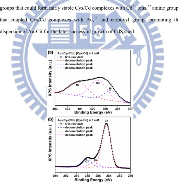
growth of sulfide nanocrystals.31 In the current synthetic system, Cys provided thiol groups that could form fairly stable Cys/Cd complexes with Cd2+ ions,32amine groups that coupled Cys/Cd complexes with Au,33 and carboxyl groups promoting the dispersion of Au-Cit for the later successful growth of CdS shell.
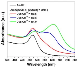
Figure 6. UV-Visible absorption spectra of Au-Cit and Au-(Cys/Cd) colloids with
various Cys:Cd2+ ratios. The concentration of Cys/Cd is 5 mM.
First, Au colloids with an average diameter of 15 nm were prepared by the citrate reduction method.34 These citrate-protected Au particles (denoted as Au-Cit) were then coupled with Cys/Cd complexes through the linkage between Au atoms and amine groups of Cys.33 This coupling event can be confirmed by the formation of nitride constituent (Au-N bonds) observed in the XPS analysis as shown in Figure 5a. Deconvolution of N1s peak produced three chemical states: the N1 component at 398.5 eV, which was assigned to a nitride constituent (Au-N), the N2 component at 399.6 eV, which resulted from the amine group of Cys (C-N), and the N3 component at 401.2 eV, corresponding to the protonated amine (NH3+) of Cys. Cys/Cd-coupled
Au nanoparticles (denoted as Au-(Cys/Cd)) showed considerable stability when dispersed in water, attributable to the electrostatic repulsion between the negatively charged carboxyl groups of Cys at the surfaces of Au as hown in Figure 5b. In the C1s region, three chemical states were also derived: the C1 component at 284.5 eV, the typical carbon in C-C bond, the C2 component at 286.7 eV, due to the carbon in C-N bond, and C3 component at 288.1 eV, coming from the carboxyl group of Cys.The stable dispersion of Au-(Cys/Cd) suspension was crucial to the later growth of CdS shell. Noted that Cys/Cd complexes were obtained by adding Cd2+ ions in Cys
solution (5 mM) in a 1:0.5 molar ratio of Cys:Cd2+. Further increase in Cd2+ amount when preparing Cys/Cd complexes caused a serious aggregation of the subsequent Au-(Cys/Cd) colloids, probably because of the pronounced coupling effect between Cd2+ and carboxyl groups of Cys and thus the loss of electrostatic stabilization. Figure 6 compares the UV-visible spectra of Au-(Cys/Cd) colloids prepared with various Cys:Cd2+ ratios. As compared to Au-Cit colloids, Au-(Cys/Cd) with a Cys:Cd2+ ratio of 1:0.5 showed a slight but not significant variation in their surface plasmon resonance (SPR) absorption characteristics. An additional absorption band at longer wavelength was however observed for Au-(Cys/Cd) when the ratio of Cys:Cd2+ was increased to 1:0.8. The presence of the long-wavelength absorption band implies that either Au particles agglomerate to some extent or a significant change in the surface chemistry of Au occurs.35 We attribute the long-wavelength absorption band of Au-(Cys/Cd) colloids to the aggregation effect which can be recognized with naked eyes from the flocculation of suspension. The long-wavelength absorption band turned dominant when Cys:Cd2+ ratio was increased to 1:1, indicating a much serious aggregation of Au-(Cys/Cd) particles therein.We chose Au-(Cys/Cd) colloids with the Cys:Cd2+ ratio of 1:0.5 as the starting material for the subsequent hydrothermal reaction to grow CdS shell. Upon the hydrothermal reaction at 130℃ for 6 h, Cys/Cd complexes, initially attached on the surfaces of Au, decomposed to yield CdS on Au surfaces, resulting in the formation of Au-CdS core-shell nanocrystals.
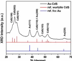
Figure 7. XRD pattern of Au-CdS nanocrystals with the reference fcc Au
(JCPDS#04-0784) and wurtzite CdS (JCPDS#06-0314) included for comparison.
Figure 8. Au-CdS nanocrystals prepared with a Cys/Cd concentration of 5 mM: (a)
low-magnification TEM images; (b) TEM-EDS elemental mapping taken on a single core-shell particle; (c) HRTEM image and (d) the corresponding SAED pattern of a single core-shell particle. The scale bar of the inset in (a) is 20 nm.
The X-ray diffraction (XRD) pattern of the product shown in Figure 7 verifies the growth of hexagonal wurtzite CdS along with fcc Au nanocrystals in the hydrothermal reaction. Figure 8a shows the typical transmission electron microscope
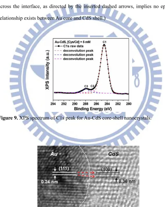
(TEM) image of the resulting composite nanocrystals. The apparent contrast between the inner core and the outer shell suggests the existence of core-shell structures. The contrast can be clearly seen in the inset of Figure 8a, from which a shell thickness of about 6 nm is observed. The composition within the composite particles was then examined using TEM-energy dispersive spectrometry (TEM-EDS). The TEM-EDS elemental mapping of Au, Cd and S shown in Figure 8b confirmed the core-shell feature of Au-CdS nanocrystals. Figures 1c and d further show the detailed crystallographic structures of the as-obtained Au-CdS core-shell nanocrystals. In Figure 8c, an HRTEM image taken at the interface of core and shell regions of a single particle, two distinct sets of lattice fringes were revealed. An interlayer spacing of 0.24 nm was observed in the core region, in good agreement with the d spacing of the (111) lattice planes of the fcc Au crystal.36 In the shell region, an interlayer spacing of 0.34 nm was however obtained, complying with the lattice spacing of the (002) planes of the wurtzite CdS.37 The corresponding electron diffraction pattern, shown in Figure 8d, further verifies the presence of both Au and CdS nanocrystals with two sets of diffraction patterns indexed as fcc Au and wurtzite CdS, respectively. This result, together with those of XRD, HRTEM, and TEM-EDS analyses, confirms the formation of Au-CdS core-shell nanocrystals by using Au-(Cys/Cd) colloids as the starting material in the hydrothermal reaction. It should be noted that the as-synthesized core-shell nanocrystals of Au-CdS retained considerably high dispersity in water, probably coming from the remaining carboxyl groups at their surfaces. Figure 9 shows the XPS peak deconvolution which revealed that three chemical states of carbon were existent: the C-C bond (C1), C-N bond (C2) and carboxyl group (C3). Furthermore, CdS-free Au particles or CdS-coated nanocrystals containing multiple Au cores were rarely observed, demonstrating the advantage of the current synthetic approach to obtain core-shell nanocrystals. The success of this
work to fabricate core-shell heterostructures was achieved by applying Cys as the trifunctional reagent in the hydrothermal process, instead the lattice parameter relationship between Au and CdS. As shown in Figure 10, a lattice mismatch of 33.3% is observed for the present Au-CdS system, implying no epitaxial relationship exists between Au core and CdS shell. (The interface between Au and CdS is highlighted by a dotted line. The abrupt transformation of the lattice arrangement across the interface, as directed by the inserted dashed arrows, implies no epitaxial relationship exists between Au core and CdS shell.)
Figure 9. XPS spectrum of C1s peak for Au-CdS core-shell nanocrystals.
Figure 10. Enlarged HRTEM image taken at the interface of Au and CdS regions on a
By controlling the experimental conditions such as the hydrothermal reaction time, the concentration of Cys/Cd complexes and the molar ratio of Cys/Cd to Au-Cit colloids, we were able to modulate the thickness of CdS shell in the range of a few to several tens nanometers. For example, a shell thickness of about 2 nm could be obtained once the hydrothermal reaction was conducted for only 1 h. On the other hand, CdS shell can grow up to 9 nm in thickness by simply raising the concentration of Cys/Cd to 10 mM while keeping the other synthetic conditions fixed. To further shell growth, we increased the molar ratio of Cys/Cd to Au-Cit colloids by increasing the volume of Cys/Cd (10 mM) added into Au-Cit colloids (9 mL, 0.25 mM). Figure 11 reveals the morphological evolution of Au-CdS nanocrystals obtained by employing 10 mM Cys/Cd of four various volumes. We depicted the correlation of Cys/Cd volumes with the resulting CdS shell thickness in Figure 11e. With increasing volumes of Cys/Cd added into Au-Cit colloids, there are increasing amount of CdS formed on the surfaces of Au nanoparticles, leading to an extensive growth of CdS shell in the resulting Au-CdS nanocrystals.
Figure 11. TEM images of Au-CdS nanocrystals prepared by employing 10 mM
Cys/Cd of (a) 1 mL, (b) 2 mL, (c) 4 mL, and (d) 8 mL. (e) Correlation of Cys/Cd volumes with the resulting CdS shell thickness.
Nanosized Au particles exhibit strong SPR absorption at around 520 nm.38 The position of SPR absorption of Au colloids depends on particle size, shape, as well as the medium surrounding them.35, 39 For example, coating Au particles with a dielectric leads to a shift in the SPR position. As shown in Figure 3a, the SPR absorption of Au colloids shifted from 520 to 553 nm after the growth of 9 nm thick CdS shell. Such an extent of SPR red-shift was consistent with the theoretical calculation result.40 The increasing thickness of CdS shell is responsible for the further red-shift in the SPR position of Au. Similar phenomenon was ever observed in Au-SiO2,41 Au-SnO2,15a and
possessing a higher refractive index led to a red-shift in the SPR position of Au. Further growth of shell thickness caused an enhancement in the overall refractive index of the medium surrounding Au, which in turn promoted the dielectric effect and resulted in more pronounced red-shift in the SPR position of Au.
According to the Mie’s theory described for core-shell particle model, a red-shift in the SPR absorption should occur to Au particles when they were encapsulated within a material of higher refractive index.43 Since the refractive index of CdS (nCdS = 2.5) is substantially larger than that of the solvent (nwater = 1.33), a significant
red-shift in the SPR absorption is expected in the core-shell nanocrystals of Au-CdS. The SPR position of Au in Au-CdS nanocrystals can be theoretically predicted using the following expression44:
(
)
⎥ ⎦ ⎤ ⎢ ⎣ ⎡ + + − = ∞ 3 2 2 2 2 2 2 2 CdS water water p n n g n ε λ λ, where n is the refractive index of the surrounding medium, ε∞
is the high frequency of Au core (ε∞
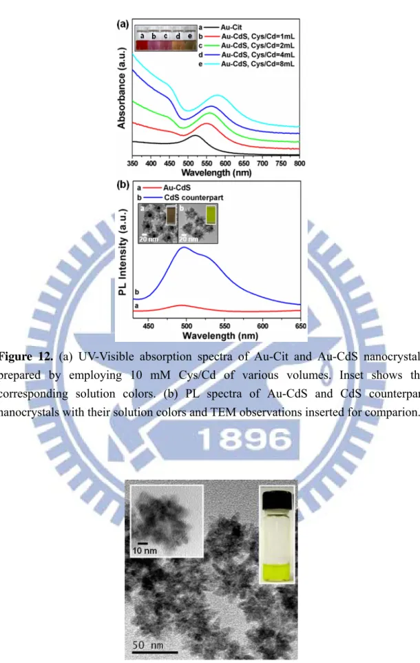
= 12.2 for Au), g is the volume fraction of shell layer, λ is the estimated SPR position, and λp is bulk plasma wavelength of Au with no medium effect (λp =139 nm for Au). The SPR positions of Au-CdS observed experimentally was in agreement with the theoretical results. For example, Au particles coated with 9 nm-thick CdS showed the SPR absorption band at 553 nm (curve b of Figure 12(a)), consistent with the theoretical value of 555 nm. In addition to the red-shift of SPR absorption, the color change of Au colloids was also evident, turning from ruby red to dark brown with increasing CdS shell thickness as illustrated in the inset of Figure 12(a). The color of Au-CdS nanocrystals turned brown because of the excitonic absorption of CdS shell, which can be recognized by the absorption onset observed at around 475 nm in Figure 12(a).
Figure 12. (a) UV-Visible absorption spectra of Au-Cit and Au-CdS nanocrystals
prepared by employing 10 mM Cys/Cd of various volumes. Inset shows the corresponding solution colors. (b) PL spectra of Au-CdS and CdS counterpart nanocrystals with their solution colors and TEM observations inserted for comparion.
Figure 13. High-magnitude TEM image of CdS counterpart nanocrystals. The insets
revealed the hollow structures of CdS counterpart and the yellow apparent color of its solution.
Core-shell nanocrystals of Au-CdS provide an ideal platform to investigate the photoinduced charge transfer property for the metal-semiconductor heterostructures. Note that Au core can serve as an effective electron scavenger for CdS shell. The Fermi level of Au is located at around +0.5V versus NHE, lower in the energetic state than the conduction band of CdS (-1.0 V vs. NHE).45 Consequently, most of the photoexcited free electrons in CdS shell would transfer to Au core, leading to the depletion of free electrons in CdS domain and the subsequent suppression of excitonic emission of CdS. Figure 12b shows the photoluminescence (PL) spectrum of the as-synthesized Au-CdS nanocrystals compared with that of CdS counterpart. CdS counterpart was prepared by treating Au-CdS nanocrystals with KCN to remove Au core, producing hollow structures of CdS as shown in Figure 13. The PL spectrum of CdS counterpart exhibited a major emission band at 495 nm and a minor shoulder at 530 nm. The band at 495 nm could be attributed to the typical excitonic band-to-band radiative emission of CdS because of its location near the absorption edge (475 nm, as determined from the absorption spectra of Figure 12a). The shoulder at 530 nm however originated from the trap-state emission.46 This trap-state emission probably came from the structural defects such as surface states produced in CdS shell during the KCN treatment. As compared to CdS counterpart, a significant quenching in the PL emission of CdS was observed for Au-CdS nanocrystals, indicating the occurrence of charge separation and electron transfer from CdS shell to Au core. This demonstration supported our argument that Au core acts as an effective electron scavenger for CdS shell.
The present Au-CdS nanocrystals also provide an ideal platform to study the interfacial charge carrier dynamics for metal-semiconductor core-shell heterostructures. Due to the difference in band structures between Au and CdS, a
pronounced photoinduced charge separation took place at the interface of Au and CdS, resulting in the electron-charged Au core and the hole-enriched CdS shell. The electron-charging of Au core in Au-CdS nanocrystals can be revealed with the corresponding XPS analysis and photocurrent measurement. As shown by the XPS spectra of Figure 14a, a binding energy of 84.1 eV of Au 4f7/2 peak was found for pure
Au colloid sample, which is in good agreement with the value of bulk metallic Au.47 However, a negative binding energy shift of around 0.5 eV of Au 4f7/2 peak was
observed for Au-CdS nanocrystals, indicating a significant difference in electronic structures between Au and CdS and a strong electronic interaction therein.48 A similar phenomenon was reported in the Au-SnO2 core-shell nanocrystal system, in which the
binding energy shift of Au 4f was attributed to the effective electron transfer from SnO2 to Au.49 Here we ascribed the negative binding energy shift of Au 4f observed in
Au-CdS nanocrystals to the electron-charging of Au core that resulted from the occurrence of charge separation.
To further elucidate the effect of Au on the charge separation of CdS for the present core-shell nanocrystals, we compared the photocurrent response of Au-CdS nanocrystal and CdS counterpart electrodes by inserting them in a photoelectrochemical cell. Note that the CdS counterpart was composed of CdS hollow structures, which were prepared by dissolving the Au core of Au-CdS nanocrystals.50 Figure 14b depicts the photocurrent generation for Au-CdS nanocrystal and CdS counterpart electrodes subjected to the white light irradiation. Both electrodes showed prompt response to the on/off cycles of light illumination, demonstrating the effective charge transfer and successful electron collection for the samples within the photoelectrochemical cell. More importantly, Au-CdS nanocrystals exhibited lower photocurrents than CdS counterpart upon light irradiation. We
believed that the significant electron transfer from CdS shell to Au core accounted for such an evident photocurrent depression found in Au-CdS nanocrystals.
Figure 14. (a) XPS spectra of Au 4f for Au colloids and Au-CdS nanocrystals. (b)
Photocurrent response of Au-CdS nanocrystal and CdS counterpart electrodes to on/off cycles of light illumination. The shell thickness of Au-CdS nanocrystals is 9.0 nm.
If the observed photocurrent depression as well as the XPS binding energy shift for Au-CdS nanocrystals indeed involved the electron transfer from CdS to Au, we should be able to reveal this event in the excitonic emission decay profile of CdS. Figure 15 represents the time-resolved PL spectra for two Au-CdS samples with different shell thicknesses. The emission decay data were analyzed with biexponential kinetics in which two decay components were derived. For Au-CdS nanocrystals with the shell thickness of 14.0 nm, emission lifetimes of both components were shorter than those of the corresponding CdS counterpart (τ1 = 0.40 ns, τ2 = 2.95 ns for
Au-CdS versus τ1 = 0.53 ns, τ2 = 2.98 ns for CdS counterpart). The intensity-average
lifetime was then calculated to make an overall comparison of the emission decay behavior.51 The difference in the average emission lifetime between Au-CdS (τ = 0.57 ns) and CdS counterpart (τ = 1.06 ns) indicates the emergence of a nonradiative pathway from the interaction between CdS and Au. This proposition can be confirmed by the emission quenching of CdS observed for Au-CdS sample.50 Such difference became more noticeable as the shell thickness of Au-CdS nanocrystals further increased to 18.6 nm (τ = 0.48 ns for Au-CdS versus τ = 1.51 ns for CdS counterpart), inferring a much more significant electronic interaction between CdS and Au. If electron transfer from CdS to Au was the predominant process that dictated the emission quenching of CdS, we can then estimate the electron-transfer rate constant (ket) of Au-CdS nanocrystals from the emission lifetime data by the following
equation: ) CdS ( 1 ) CdS Au ( 1 > < − − > < = τ τ et k
Using the lifetime values listed in Table 1, we obtained the electron-transfer rate constants as 0.36 × 10⁹, 0.51 × 10⁹, and 1.42 × 10⁹ s-1 for Au-CdS nanocrystals with the shell thickness of 9.0, 14.0, and 18.6 nm, respectively.
Figure 15. Time-resolved PL spectra of Au-CdS nanocrystals and CdS counterpart
with the shell thickness of (a) 14.0 nm, and (b) 18.6 nm. The fitting results (solid curves) were also included for comparison. Insets show the corresponding TEM images and the scale bar is 20 nm.
Table 1. Kinetic analysis of emission decay for Au-CdS nanocrystals with various
shell thicknesses and their corresponding CdS counterparts.
entry A1 τ1 (ns) A2 τ2 (ns) <τ> (ns) ket (s-1) Au-CdS, 9.0 nm 9843.3 0.37 60.9 2.58 0.46 CdS counterpart 11532.9 0.41 102.0 2.91 0.56 0.36 × 10⁹ Au-CdS, 14.0 nm 11539.6 0.40 110.7 2.95 0.57 CdS counterpart 9512.3 0.53 464.4 2.98 1.06 0.51 × 10⁹ Au-CdS, 18.6 nm 10633.5 0.39 49.4 2.99 0.48 CdS counterpart 9873.0 0.58 599.0 3.82 1.51 1.42 × 10⁹
It should be noted that the electron-transfer rate constant of Au-CdS nanocrystals increased with increasing shell thickness. The less pronounced interaction between electrons and holes in the thicker CdS shell may contribute to such an increase in electron-transfer rate constant for Au-CdS nanocrystals with increasing shell thickness. We noticed that the emission lifetimes of the three CdS counterpart samples were substantially different, with CdS of larger characteristic size (thickness) showing longer emission lifetime, as can be seen in Table 1. This size-dependent correlation of exciton lifetime has been widely reported for CdS nanocrystals.52 It is generally believed that the significant interaction between electrons and holes, which is due to the confinement of electrons and holes in a particle of reduced size, may induce additional pathways for nonradiative recombination.53 A shortened exciton lifetime would consequently be observed for CdS nanocrystals with reduced size. The electron-hole interaction in small particles is related to the trapping of excitons by the abundant surface states that may further act as alternative sites for nonradiative charge recombination.54 For the present Au-CdS nanocrystals, it is reasonable to presume a less pronounced electron-hole interaction for Au-CdS with thicker CdS shell since they possessed a larger characteristic size of CdS and thus a smaller number of surface states. Such less pronounced electron-hole interaction in fewer surface states prohibited charge carriers from being consumed in nonradiative recombination, which further enabled a fuller extent of participation of photoexcited electrons in the charge separation process. Accordingly, an increase in the electron-transfer rate constant was observed for Au-CdS nanocrystals with increasing shell thickness.
Since Au-CdS nanocrystals exhibited pronounced charge separation upon light illumination, it is worth studying the potential application that this property may bring. Owing to the effective electron transfer from CdS shell to Au core, photogenerated
holes of an abundant amount were existent in CdS shell and would transfer to the surfaces of Au-CdS nanocrystals. These highly reactive holes could oxidize water to produce hydroxyl radicals that can further decompose organic pollutants through an oxidation process. A spectacular capability of photocatalytic oxidation is therefore expected at the surfaces of Au-CdS nanocrystals. A series of photocatalysis experiments were performed in this work to investigate the photocatalytic properties of the as-synthesized Au-CdS nanocrystals. RhB, a typical dye that can be decomposed by hydroxyl radicals,55 was used as the test pollutant to monitor the photocatalytic oxidation progress for Au-CdS nanocrystals. The time-dependent UV-visible spectra of RhB solutions under visible light illumination in the presence of Au-CdS nanocrystals with a shell thickness of 14.0 nm were first shown in Figure 16a. It can be seen that the intensity of the characteristic absorption peak at 553 nm decreased dramatically with the irradiation time. Besides, a concomitant blue shift in the absorption maximum was observed after the solution was irradiated for 20 min. It is well-known that the photodegradation of RhB undergoes two competitive processes.56 One is the destruction of dye chromogen, which is characteristic of the loss of absorbance at 553 nm. The other is the N-demethylation reaction that produces a series of N-demethylated intermediates, accompanied by a blue shift in the absorption maximum from 553 to 498 nm. In the current case, RhB concentration was determined by referring to the absorbance of the characteristic peak at 553 nm. To quantitatively understand the reaction kinetics of RhB photodegradation for our samples, we analyzed the normalized concentration of RhB (C/C0) as a function of irradiation time. As shown in the inset of Figure 16a, an exponential decay of RhB concentration with the irradiation time was evident for Au-CdS nanocrystal photocatalyst. The photodegradation process was then fit to pseudo-first-order reaction, in which the value of the apparent rate constant (kRhB) is equal to the slope of
the fitting line according to the following expression:57 ln(C/C0) = -kRhBt, where C0
and C are the concentrations of RhB at initial and at a certain irradiation time t, respectively.
For Au-CdS nanocrystals with a shell thickness of 14.0 nm, kRhB is found to be
0.026 min-1. The mechanism for RhB photodegradation by using Au-CdS nanocrystal photocatalyst can be described by the following four pathways:
Au–CdS + hν Æ Au(e–)–CdS(h+) (1)
Au(e–)–CdS(h+) + H2O Æ Au(e–)–CdS + H+ + ·OH (2)
RhB + ·OH Æ oxidation products (3) Au(e–)–CdS + O2 Æ Au-CdS + ·O2– (4)
Under visible light illumination, charge separation occurred within Au-CdS nanocrystals, resulting in an electron-charged Au core and a hole-enriched CdS shell (eq 1). Subsequently, the photogenerated holes transferred to the surfaces of nanocrystals and reacted with water to produce hydroxyl radicals (eq 2). RhB molecules were then decomposed by hydroxyl radicals through an oxidation process (eq 3). Once the photogenerated holes were depleted in photocatalysis, Au-CdS nanocrystals underwent a Fermi level equilibration due to the accumulation of photoexcited electrons.4 Note that experiments of RhB photodegradation were conducted in air. The exposure to air during the operation of photocatalysis can discharge the accumulating electrons of Au-CdS nanocrystals to the dissolved oxygen,14c, 15b which resulted in a neutralized state of nanocrystals that are allowed for further photoexcitation (eq 4).
Figure 16. (a) Absorption spectra of RhB solutions under different irradiation times
by using Au-CdS nanocrystals with the shell thickness of 14.0 nm. Inset shows the ln(C/C0) versus irradiation time plot with the fitting result included. (b) C/C0 versus irradiation time plots for RhB photodegradation without any catalyst and in the presence of Au-CdS nanocrystals with various shell thickness.
The photocatalytic performance of Au-CdS nanocrystals with three various shell thicknesses was then compared in Figure 16b. It should be noted that experiment in the absence of photocatalyst showed almost no RhB photodegradation, implying that the self-photolysis of RhB is negligible under visible light illumination. For Au-CdS
nanocrystals with a shell thickness of 9.0 nm, about 50% of RhB was degraded after 40 min of irradiation. A higher extent of RhB photodegradation to around 70% at the same irradiation time was achieved when using Au-CdS nanocrystals with a thicker shell of 14.0 nm. For Au-CdS nanocrystals with the shell thickness of 18.6 nm, RhB was almost completely decomposed after 40 min of irradiation. From the above observations, we concluded that the photocatalytic activity of Au-CdS nanocrystals was enhanced with increasing shell thickness. This is mainly a result of the extensive growth of CdS shell in Au-CdS nanocrystals. With increasing shell thickness, a raised ratio in the amount of CdS to Au was attained, leading to a greater capability of light absorption for Au-CdS nanocrystals and thus the generation of more charge carriers. This argument can be verified by the fact that the excitonic absorption of CdS for Au-CdS nanocrystals turned significant with increasing shell thickness.50 Consequently, a higher number of photoexcited charge carriers was expected for Au-CdS nanocrystals with larger shell thickness, which in turn promoted the resulting photocatalytic efficiency toward RhB photodegradation. It is worth noting that the increase in photocatalytic activity of Au-CdS nanocrystals with the increasing shell thickness corresponded well with the result of electron-transfer rate constant variation, which could be realized by the causal relation between electron transfer and hole generation. As the shell thickness of Au-CdS nanocrystals increased, more and more photoexcited electrons transferred from CdS shell to Au core, simultaneously leaving photogenerated holes of an increased amount in CdS shell. The rise in the number of photogenerated holes further led to the enhancement in the resulting photocatalytic performance as observed. For more clarity on this relation, we depicted the correlations of electron-transfer rate constant (ket) and rate constant of RhB
Figure 17. Correlations of electron-transfer rate constant (ket) and rate constant of
RhB photodegradation (kRhB) with the shell thickness of Au-CdS nanocrystals.
Further comparative experiments were conducted to demonstrate the superior photocatalytic performance for the present Au-CdS nanocrystals. Four kinds of photocatalysts including N-doped P-25 TiO2, commercial CdS powders, CdS
counterpart, and Au-CdS nanocrystals were used in the photodegradation of RhB under the same experimental conditions. The comparative results were shown in Figure 18a, from which several points can be observed. First, as compared to the relevant commercial products like N-doped P-25 TiO2 and CdS powders, Au-CdS
nanocrystals exhibited superior photocatalytic performance under visible light illumination, demonstrating their potential as an efficient visible-light-driven photocatalyst in relevant redox reactions. Second, Au-CdS nanocrystals performed better toward RhB photodegradation than CdS counterpart, which can be accounted for by the pronounced charge separation that occurred at the interface of Au and CdS. This demonstration addresses the benefit of the present metal-semiconductor core-shell nanocrystals to photocatalytic applications. To further explore the applicability of the as-synthesized Au-CdS nanocrystals in a more practical situation,
their photocatalytic performance under natural sunlight was also evaluated. As illustrated in Figure 18b, after exposure to 150 min of daytime sunlight, 90% of RhB was degraded by using Au-CdS nanocrystals, accompanied by an evident decoloration of the resulting solution. This result shows that the present Au-CdS nanocrystals can be used as highly efficient photocatalysts which may practically harvest energy from sunlight.
Figure 18. (a) C/C0 versus irradiation time plots for RhB photodegradation in the
presence of different photocatalysts. (b) Absorption spectra of RhB solutions after exposure of 150 min of daytime sunlight without any catalyst and in the presence of Au-CdS nanocrystals with the shell thickness of 18.6 nm. Insets show the corresponding solution color.
2-3.2 Au-Cd1-xZnxS Core–Shell Nanocrystals
Recyclability is an important issue to be considered for semiconductor photocatalysts. For the current Au-CdS nanocrystals, the photocatalytic activity was significantly depressed if the sample was repeatedly used in photocatalysis. This is due to the photocorrosion that occurred at the surface of CdS under light illumination in the presence of oxygen and water:60
CdS + 2O2 Cd2+ +SO4
2-In order to enhance the durability performance during their use as photocatalyst, the photocorrosive oxidation of Au-CdS nanocrystals must be prevented. As an efficient photocatalyst as well, ZnS possess much more positive valence band potential than CdS, which makes it more photocorrosion-resistant than CdS. To improve the recyclability when used as photocatalysts, we introduced Zn into the CdS shell of Au-CdS to form Au-Cd1-xZnxS nanocrystals. The sample was synthesized by
co-feeding Cd and Zn precursors in the hydrothermal reaction. Figure 19a shows the morphology of the resulting Au-Cd1-xZnxS nanocrystals with the precursor ratio of
Cd2+:Zn2+ of 1:4. The resulting morphology is similar to Au-CdS nanocrystals and also shows great dispersity in aqueous solution. The composition at the core (the region of the yellow circle in the inset of Figure 19a) and the shell (the region of the red circle in the inset of Figure 19a) was examined using TEM-EDS and the result was shown in Figure 19b. The relative atomic ratio at the core region is 0.22:0.28:0.16:0.34 for Au:Cd:Zn:S, and the composition at shell region is 0.05:0.24:0.34:0.37 for Au:Cd:Zn:S. In Figure 19c, as compared to Au-CdS nanocrystals, the SPR absorption of Au for Au-Cd1-xZnxS was slightly red-shifted,
which resulted from the higher refractive index of ZnS (n=2.57) than CdS (n=2.51).61 According to the theoretical calculation, the Au SPR would red-shift to about 3nm if
CdS shell is totally replaced by ZnS with the same shell thickness. Thus, the slightly red-shift observed in Figure 19b is consistent with the theoretical calculation result.
Figure 19. (a) TEM image of Au-Cd1-xZnxS nanocrystals prepared with the precursor
ratio of Cd2+:Zn2+ of 1:4. Inset shows the region taken for TEM-EDS measurement and the scale bar is 5 nm. (b) UV-Visible spectra of Au-CdS and Au-Cd1-xZnxS
nanocrystals.
The recyclability of Au-Cd1-xZnxS nanocrystals was evaluated by repeatedly
compared here were with shell thickness of 18.6 nm since Au-CdS nanocrystals with this shell thickness performed the best in the RhB photodegradation. In Figure 20, at the fifth injection of RhB, Au-CdS sample could decompose about 50% of RhB, while Au-Cd1-xZnxS did much better by reducing at least 80% of RhB under the same
condition. Therefore, the recyclability of Au-CdS nanocrystals was effectively improved through doping Zn into CdS shell.
Figure 20. C/C0 ersus irradiation time plots for RhB photodegradation in the presence
of (i) Au-CdS and (ii) Au-Cd1-xZnxS nanocrystals.
2-3.3 Au-ZnS Core–Shell Nanocrystals
The synthetic procedure of Au-CdS nanocrystals can also be applied to obtain Au-ZnS core-shell nanocrystals with controllable thickness. The shell thickness can be tuned by employing different volumes of Au-Cit. Figure 21 shows the morphology of Au-ZnS nanocrystals with the shell thickness of 53.8, 32.3, 27.7, and 24.0 nm by employing 4.5, 9, 18 and 36 mL of Au-Cit, respectively. The shell thickness decreased with increasing volume of Au-Cit, and was much thicker than Au-CdS nanocrystals
since the concentration of precursor is 10 times higher (100 mM for Cys/Zn and 10mM for Cys/Cd). For the sample with 36 mL ofAu-Cit (Figure 21d), some particles that have more than one Au core can be observed.
Figure 21. TEM images of Au-ZnS nanocrystals prepared by employing Au-Cit of (a)
4.5, (b) 9, (c) 18, and (d) 36 mL.
In addition to the photocatalytic degradation of dye molecules, metal-semicomductor core-shell nanocrystals can be further applied in relevant photoelectrochemical processes such as photocatalytic methanol oxidation. It is well known that an additional bias is needed to be applied in photoelectrochemical cell to trigger the chemical reaction.62 With the concern of energy conservation nowadays, it will be more desirable if the photocatalysts or photoelectrodes can work just by light illumination without applying bias. Since Au-ZnS nanocrystals are full of positively charged holes at their surfaces upon light illumination, a considerably high oxidizing