Watermarking for intellectual
property protection
Y.C. Fan and H.W. Tsao
A new watermarking method for intellectual property (IP) protection is presented. The proposed method uses a uniquely generated stream of bits, known as a watermark, embedded into the self-test circuit to represent ownership. This scheme can detect the ownership rights of the IP provider even when the chip has been packaged. Experimental results show the proposed embedding technique can survive synthesis, placement and routing. The experimental results are given to demon-strate the proposed method.
Introduction: Advances in semiconductor processing technology have led to a rapid increase in IC design complexity. Intellectual property (IP) based design has become a major concern in IC industries[1]. The protection of IP has also received a great deal of attention recently. A number of IP protection techniques, which embed watermarks at the physical design level, have been proposed[2–4]. However, these techniques are not adequate to protect the ownership rights of the soft IP core. After synthesis, placement and routing, the layout of the soft IP core is changed. In addition, it is also difficult to detect the ownership rights of the IP provider after the chip has been packaged. The IP designer must examine a photomicrograph to check the ownership rights. It is often inconvenient to do so. To solve these problems, this Letter proposes a new watermarking method at the behavioural level to protect the IP core.
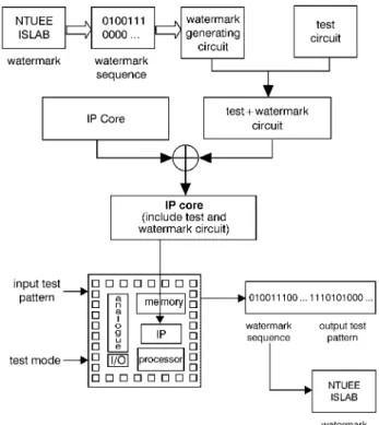
IP watermarking: According to the Virtual Socket Interface (VSI) Alliance reusable rule, IPs will keep the test circuits after integrating the IPs into full systems-on-a-chip (SOC)[1]. The designer provides the test vectors to verify the function of the IPs. After integrating the IPs into full SOCs, the only signal in an IP that can be traced is the test signal. If the test circuit is combined with a watermark generating circuit, the ownership rights of the IP provider can be secured easily in the test mode. This involves performing a watermarking-based IP core protection procedure (Fig. 1). First, the digital watermark is designed, and it represents the owner of the IP (may be an organisation logo, or designer’s signature, etc). A watermark generating circuit is designed to generate the watermark as a binary pattern. Next, the test circuit is combined with the watermark generating circuit. When the chip is put in test mode, it will send out the watermark sequence and test patterns. Based on the watermark sequence, the ownership rights of the IP provider can be verified.
Fig. 1 ‘Watermarking based IP core protection’ design flow
The architecture of the circuit is shown in Fig. 2. The watermark generating circuit is composed of a parallel in serial out (PISO) register and several inverter gates. When this chip is put in test mode, the ‘test mode signal’ controls the watermark generating circuit and test circuit. The parallel watermark data is generated when the test mode signal is active. The PISO translates the parallel watermark data into a serial watermark sequence. Then the chip sends out the watermark sequence first then followed by the test pattern. According to the watermark information, the IP provider is able to verify the ownership rights and does not need to examine the photomicrograph.
Fig. 2 Architecture of watermark generating circuit
Fig. 3 Layout of unwatermarked circuit
Fig. 4 Layout of watermarked circuit
Experimental results: A set of experiments has been performed to verify the feasibility of this proposed procedure. Results are given for an example chip, a video format converter, which contains several IPs. A watermark-generating circuit has been designed to generate 20-bit watermark sequences and it is integrated into the video format converter chip.Fig. 3shows the layout of the unwatermarked circuit, andFig. 4shows the layout of the watermarked circuit. The water-mark generating circuit is hidden in the whole chip, and it cannot
ELECTRONICS LETTERS
4th September 2003
Vol. 39
No. 18
render a visible artifact in the layout view. (Fig. 4). In this example, the chip just uses 207 gates (only a 0.13% increase for this chip) to implement the watermark-generating circuit. Our proposed methods thus have a low hardware cost. Since the watermark is embedded into the test circuit at the behaviour design level, the watermark function is not changed after synthesis. No matter what kind of synthesis constraint is used, the watermark sequence can still be extracted correctly. After placement and routing, the ownership rights can still be detected according to the watermark sequence. It is also easy to detect the ownership rights of the IP provider after the chip has been packaged. The experimental results demonstrate that our proposed embedding technique does achieve the goal.
Conclusion: In this Letter, we show that a new watermarking scheme for IP protection has been developed for any digital circuit design. This watermarking method has been successfully implemented in real circuits. Experimental results have confirmed the efficiency of the scheme. Our proposed method has a low hardware cost (only a 0.13% increase for the example chip) and is easy to implement. The proposed embedding technique can survive synthesis, placement and routing. We can verify ownership rights after integrating several IPs into full SOCs. The proposed method thus indeed has the potential to solve the IP protection problem.
#IEE 2003 13 June 2003
Electronics Letters Online No: 20030874 DOI: 10.1049/el:20030874
Y.C. Fan and H.W. Tsao (Department of Electrical Engineering and Graduate Institute of Electronics Engineering, National Taiwan University, Taipei 10617, Taiwan, Republic of China)
E-mail: d9921004@cc.ee.ntu.edu.tw
References
1 CHANG, H.: ‘Surviving the SOC revolution: a guide to platform-based design’ (Kluwer Academic Publishers, 1999), pp. 1–30
2 KAHNG, A.B., MANTIK, S., MARKOV, I.L., POTKONJAK, M., TUCKER, P.,
HUIJUAN WANG and WOLFE, G.: ‘Robust IP watermarking methodologies for physical design’. Design Automation Conference, 1998. Proceedings, 1998, pp. 782–787
3 NARAYAN, N.,NEWBOULD, R.D., CAROTHERS, J.D., RODRIGUEZ, J.J., and
HOLMAN, W.T.: ‘IP protection for VLSI designs via watermarking of routes’. ASIC=SOC Conference, 2001. Proceedings. 14th Annual IEEE International, 2001, pp. 406–410
4 NEWBOULD, R.D., IRBY, D.L., CAROTHERS, J.D., RODRIGUEZ, J.J., and
HOLMAN, W.: ‘Watermarking ICs for IP protection’, Electron. Lett., 2002, 38, (6&14), pp. 272–274