氮化鋁鎵薄膜表面微結構之近場光學特性
77
0
0
全文
(2) 氮化鋁鎵薄膜表面微結構之近場光學特性 Near-Field Optical Properties of Microstructures on AlGaN Thin Films. 研 究 生:馮逸文. Student:I-wen Feng. 指導教授:李明知博士. Advisor:Dr. Ming-Chih Lee. 國 立 交 通 大 學 電子物理系 碩 士 論 文. A Thesis Submitted to Department of Electrophysics College of Science National Chiao Tung University in partial Fulfillment of the Requirements for the Degree of Master of Physics in Electrophysics July 2005 Hsinchu, Taiwan, Republic of China. 中華民國九十四年七月.
(3) 氮化鋁鎵薄膜表面微結構之近場光學特性. 國立交通大學電子物理學系碩士班 研究生:馮逸文. 指導教授:李明知博士 中文摘要. 本論文主要針對有機化學氣相磊晶系統 (MOCVD system) 所成長 的氮化鋁鎵薄膜表面上微結構作一系列的近場光譜分析。氮化鋁鎵薄 膜成長於不同材料的緩衝層 (buffer layer) 上,因薄膜所受的應力 不同,表面會形成形貌相異之微結構。不同類型的六角丘狀 (Hexagonal hillock) 結構出現於以氮化鋁作緩衝層的樣品上,而 V 形缺陷則可在以氮化鎵作緩衝層的樣品上觀察到。針對不同類型的六 [1],[2]. 角丘狀結構和平坦處比較,譜峰位置會有紅移,之前已有論文. 指. 出這現象是因不同的鋁組成分佈所造成的。然而,從近場光譜分析可 知,隨著不同類型的六角丘狀結構,其光學特性和其表面形貌也有其 特殊的相關性。而另一樣品上 V 形缺陷則可觀察到額外的發光譜峰 (~3.578eV) ,有別於近帶躍遷的譜峰位置(~3.693eV) ,有文獻指 [3]. 出此能階是由鎵空缺所造成的 。本論文中利用近場光學顯微鏡 (NSOM) 就單一不同形貌六角丘狀結構以及 V 形缺陷作光學性質之分 析。. i.
(4) Near-Field Optical Properties of Microstructures on AlGaN Thin Films. Student: I-wen Feng. Advisor: Dr. Ming-Chih Lee. Institute of Electrophysics National Chiao Tung University ABSTRACT In this article, we analyzed the optical properties of the microstructures on AlGaN films with near-field scanning optical microscopy (NSOM). Different types of hillocks (mesa-like, tent-like, and pyramid-like) appeared on the film with AlN buffer layer while V-shape pit formed in the sample with GaN buffer layer. In the NSOM spectra, the emission from the apexes of hillocks of different types of hillock is red-shifted in comparison with that from the plain surface. It may be due to the fluctuation of Al content. [1], [2]. . Since the spatial resolution. of NSOM (~100 nm) is capable of observing different regions inside single hillock. The luminescence from various probed. ii.
(5) regions on different types of hillock reflects their properties in detail. The spectra showed an extra peak (~3.578eV)from the V-shape pit that differs from the near-band edge emission ( ~ 3.693eV ) . We suggested that this emission could be attributed to Ga vacancy. [3]. . From the intensity-mapping image,. Ga vacancies seemed to be accumulated at the pit.. iii.
(6) 致謝 『準備適合幸運降臨的環境, 不能只顧一己的私利。 創造環境, 與他人共享共贏才能帶來幸運。』. ──幸運守則第四條 From 《GOOD LUCK——當幸運來敲門》 Fernando Trias de Bes & Alex Rovira Celma 著. 研究所這兩年,其中經過一次系館的搬遷,由於大家的合作使得 實驗室能在短期內一切順利就緒,也因為大家的幫忙,論文才得以完 成。這一切的幸運要感謝李明知老師、陳衛國老師與周武清老師的教 導與教誨,學長古慶順、張富欽、柯文政、李寧、陳京玉、傅振邦、 蔡伩哲、顏國錫、何志偉的協助與指導,同學沈承勳、林碧軒、黃鐘 逸、黃佳進、陳信志的支持與勉勵,以及學弟妹邱泰鑫、李啟仁、戴 士凱、洪維偲、羅士傑、張尚樺、包家禎的關心與陪伴。 最後,感謝父母與家人,因為他們的支持,讓我能專心的完成學 業。 逸文, 2005/07. iv.
(7) Content Abstract (Chinese version)……………………………………… ⅰ Abstract (English Version)……………………………………… ⅱ 致謝…………………………………………………………………… ⅳ 1. Introduction……………………………………………………… 1. 2. Theoretical Backgrounds ……………………………………… 3 2.1 Wurtzite Structure………………………………………… 3 2.2 Photoluminescence (PL)…………………………………… 5. 3. Experimental Details ………………………………………… 11 3.1 Sample. Preparation………………………………………11. 3.2 Atomic Force Microscopy (AFM) …………………………13 3.3 Micro-PL (μ-PL) ………………………………………… 15 3.4 Near-Field Scanning Optical Microscopy (NSOM)……17 4. Results and Discussion …………………………………………22 4.1 Surface Morphology of AlGaN Films ………………… 22 4.2 Optical Property of Hillock …………………………… 31 4.3 Optical Property of V-shape pit……………………… 62. 5. Conclusion ……………………………………………………… 66. Reference …………………………………………………………… 68. v.
(8) 1 Introduction Light-emitting diodes (LEDs) based on Ⅲ -nitrides have received much industrial and research interest in the past few years. However, Ⅲ-nitride films are usually grown on sapphire substrates and the high lattice mismatch between the substrate and the epilayer leads to the formation of crystal defects, such as stacking faults, dislocations, pits, hillocks ,and etc. In this study, the defects of V-pits and hillocks will be instigated in detail. Hillocks and V-pits have been observed in metalorganic chemical vapor deposition (MOCVD) grown films. [1]-[12]. . The. hillocks forms when the films are under compressive stress. [11]. while the pits are usually formed from threading dislocations, which are generated by plastic relaxation. [4]. . In addition,. several authors have studied the optical or electric properties of the two microstructures on Ⅲ-nitrides. [4]-[12]. .. In this thesis, special emphasis is put on the study of the correlation between the optical properties and topography of the two microstructures. In our previous study, we utilized. 1.
(9) micro-PL to analyze the properties of hillocks and V-pits on the AlGaN films. [1]-[3]. . However, the spatial resolution of. micro-PL is 2-3 μm. To achieve better resolution, near-field scanning optical microscopy (NSOM) has beenemployed. The spatial resolution of our NSOM system is about 100 nm and the mapping technique may provide clear correlation between the emission efficiency and topography. Thus, we will investigate the different facets or regions on all types of hillocks or inside V-pits in the AlGaN films with high-resolution NSOM PL system.. There are five chapters in the thesis, including this chapter, Introduction. In Chapter 2, we briefly describe the structure and the optical transitions of Ⅲ -Nitride semiconductors. In Chapter 3, we illustrate the sample preparation and the experimental setup. Chapter 4 shows the results, including the surface morphology and near-field optical properties of hillocks and V-pits. Finally, in chapter 5, we summarize the relationship between optical properties and topographies of both two microstructures. 2.
(10) 2 Theoretical Backgrounds 2-1 Wurtzite structure The common crystal structures for group-III nitrides are wurtzite and zincblende structures, as shown in Figure 2.1.1, in which wurtzite structure is more stable at ambient condition. Wurtzite structure consists of two hexagonal close packed sub-lattices, each with one type of atoms, and the two are offset along the c axis by 5/8 of the cell height. The stacking sequence of (0001) planes is ABABAB in the <0001> direction and each group-III atom is coordinated with four nitrogen atoms while each nitrogen atom is coordinated with four group-III atoms. The two lattice constants, c and a, are 4.9816 Å and 3.1130 Å for AlN, and 5.1851 Å and 3.1893 Å for GaN, respectively. For AlGaN, the lattice constants could be obtained according to the Vegard’s law. [13]. :. c0 ( x) = c0GaN (1 − x) + c0AlN x, a 0 ( x) = a 0GaN (1 − x) + a 0AlN x,. 3.
(11) Fig.2.1.1 (a) The Zinc-Blende structure and (b) the Wurtzite structure of Ⅲ-nitride. (http://www.univ-lemans.fr). 4.
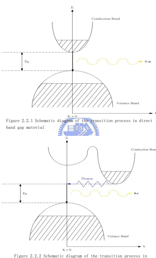
(12) 2.2 Photoluminescence (PL) Photoluminescence is a non-destructive technique for characterizing material parameters, such as impurity level, band-gap, activation energy and etc. The luminescence involves three. processes. -. excitation,. thermalization,. and. recombination. When incident radiation of sufficient energy is absorbed by sample, electron-hole pairs are produced and re-distributed to a state of quasi-thermal equilibrium. Then, electron-hole pairs recombine and may release the excess energy by emitting photons. However, recombination can be categorized into two groups, radiative and non-radiative transitions. I.. Radiative transitions. A. Interband recombination Interband luminescence corresponds to the annihilation of electron-hole pairs. An electron that has been excited to the conduction band returns into a hole in the valance band with emission of a photon. If the conduction band minimum and the valance band maximum occur at the same point in K-space, which is known as “direct band gap” (Figure 2.2.1), the probability. 5.
(13) for radiative electron-hole recombination will be high. Therefore, the radiation lifetime may be short and the luminescent. efficiency. is. expected. to. be. high.. The. recombination rate is determined as R = ∫ R(hν )d (hν ) ≈ np ,. where n is electron concentration and p is hole concentration. The condition is met in most Ⅲ-Nitrides (such as GaN, InGaN, AlGaN). On the other hand, in indirect band gap materials, the conduction band minimum and the valance band maximum are at the different points in K-space (Figure 2.2.2). Then, for conservation of crystal momentum, a phonon must participate in the process with a relatively small transition probability. Therefore, the radiation lifetime is much longer and the luminescent efficiency is quite smaller than those of direct band gap materials. For instance, silicon has indirect band gap and thus not common as light emitter.. 6.
(14) Figure 2.2.1 Schematic diagram of the transition process in direct band gap material. Figure 2.2.2 Schematic diagram of the transition process in indirect band gap material 7.
(15) B. Exciton recombination The inclusion of Coulomb interaction between the electrons in the conduction band and holes in the valance band results in the formation of excitons. As a result, less transition energy are involved in the exciton recombination process than in the band gap transition: E x = E g − En , mr2 e 4 1 where Eg is the band gap energy, En ( = 2 2 ⋅ 2 )is the binding 2ε 0 h n. energy of electron-hole pairs, mr is the reduced mass and n is the quantum number. The exciton may be classified into two types, Wannier exciton and Frenkel exciton, depending on its Bohr radius. In Wannier exciton, the distance between the electron and hole is larger than the lattice constant. In contrast, the Bohr radius of Frenkel exciton is almost the same order of, or smaller than, the lattice unit. In our studies, Wannier exciton exists in most of nitride semiconductors. In addition, free excitons sometimes may be bound to donors or acceptors, especially in imperfect crystal. The bound. 8.
(16) exciton energy is lower than the free exciton energy: Ebx = E g − E n − E B = E x − E B. where EB is the binding energy of the exciton to the donor (or the acceptor). C. Donor-acceptor pair recombination When the concentration of both donors and acceptors is high, the recombination involving donor-acceptor pairs is pronounced. The transition energy, with the separation distance r between +. -. ionized donor (D ) and acceptor (A ), can be expressed by Coulomb interaction and described as hω = E g − (E D + E A ) +. e2 , εr. where Eg is the band gap energy, ED and EA are the binging energy of the donor and the acceptor, respectively. In addition, the radiative rate also depends on the separation distance: R DA (r ) = R DA (0) exp(−2r / a ) ,. where a is the Bohr radius of the shallow impurity in the pair. Therefore, the recombination rate and the PL intensity decrease quickly with great distance r.. 9.
(17) II.. Non-radiative transitions. Generally speaking, the photoluminescent efficiency can be expressed as η=. 1/τ r , 1 / τ r + 1 / τ nr. where τr andτnr are lifetimes of radiative and non-radiative recombination,. respectively.. Therefore,. non-radiative. recombination centers, as due to any imperfection of the crystal, result in reducing the intensity of photoluminescence. The excited carrier may recombine non-radiatively through such processes: A. Shockley-Read-Hall recombination process An allowed energy state, due to a deep trap, within the forbidden band gap may act as a recombination center. B. Auger recombination process An electron and a hole may recombine and release energy that is absorbed by a third particle in materials (such as a free electron or a free hole) with high doping concentration.. 10.
(18) 3 Experiment Details 3.1 Sample Preparation All AlGaN films studied in this work were grown in a horizontal. low-pressure. metal. organic-chemical. vapor. deposition (MOCVD) reactor, AIXTRON 200. This system is equipped with RF-heating module. Trimethylgallium (TMGa), trimethylaluminum (TMAl), and ammonia (NH3) were used as the source precursors for Ga, Al, and N, respectively, with H2 carrier gas. (0001) Sapphire was used as substrate. Prior to the growth of buffer layer, thermal cleaning was carried out in the growth chamber for 10 minutes at 1120 ℃ under H2 flow in order to remove impurities on the surface of sapphire. Two AlGaN films with different growth conditions have been studied. The growth parameters of the first one, Sample A, are described as below: A thin (~25nm) nucleation layer of AlN was grown at 650 ℃ for minimizing the lattice mismatch between the AlGaN thin film and sapphire. Then, the temperature was raised to 1120 ℃ to grow AlGaN layer about 0.8 μm. For Sample B, 25 nm GaN, which was grown at 520 ℃, was used. 11.
(19) as the nucleation layer. After increasing the temperature to 1120 ℃, the GaN layer of 2μm was grown as the buffer layer and then 0.7 μm layer of AlGaN was deposited.. 12.
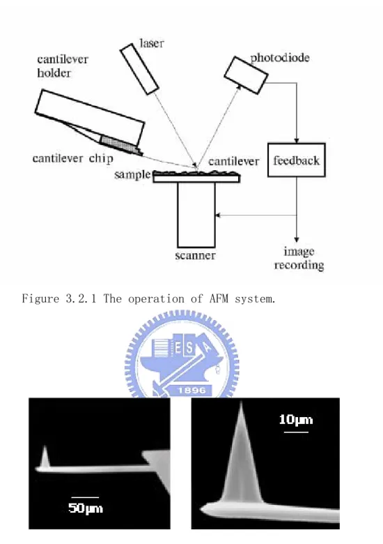
(20) 3.2 Atomic Force Microscopy (AFM) [14]. Gerd Binning and Calvin F. Quate invented AFM in 1986 . They realized that it is able to measure interactive force between atoms of the tip and sample surface by using special probe which consists of a flexible, elastic cantilever and sharp probe tip. Figure 3.2.1 shows the typical configuration of AFM. The interaction between the tip and the sample may repel or attract atoms of the tip and results in bending of cantilever. Therefore, it is capable of evaluating the motion of the tip by detecting the deflection of laser beam, which is reflected from the back of the cantilever. In this way, the morphology of sample surface can be obtained by mapping out roughness step-by-step. AFM can be operated in contact, non-contact, or tapping mode. Among them, tapping mode minimizes the surface damage. In our study, the morphology measurement was performed in tapping mode by using Solver P47H developed at NT-MDT. The probe was also manufactured by NT-MDT with a cantilever and a sharp tip, whose radius of curvature is ~10 nm (Figure 3.2.2).. 13.
(21) Figure 3.2.1 The operation of AFM system.. Figure 3.2.2 The SEM image for scanning probe of AFM system. (http://www.ntmdt.ru). 14.
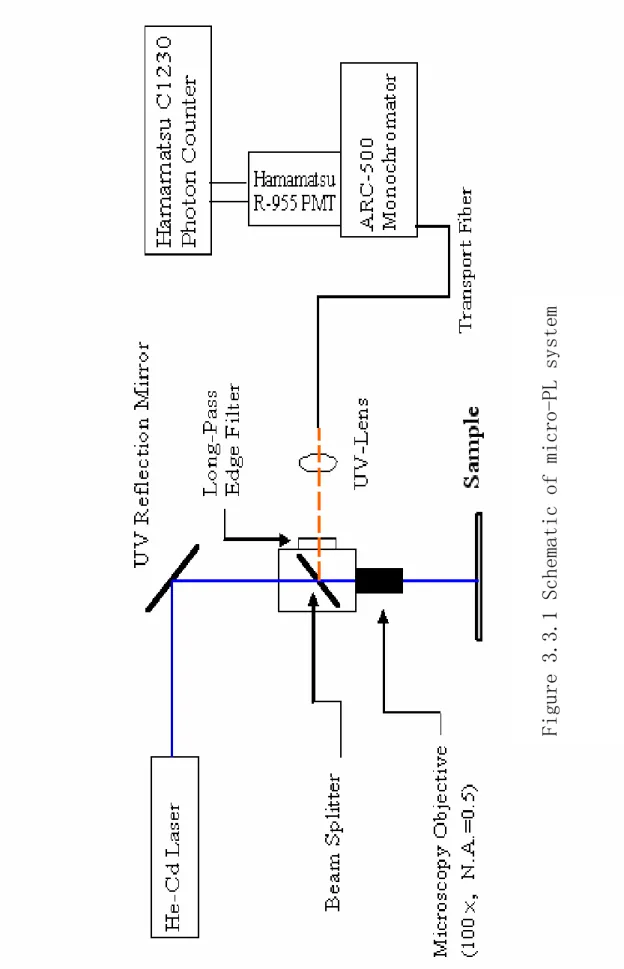
(22) 3.3 Micro-Photoluminescence (μ-PL) Figure 3.3.1 shows our room temperature micro-PL system. He-Cd laser beam (which is operated at 325 nm) was focused through a microscope objective (100×, 0.5 N.A) on the samples (where the spot-size was about 2-3μm) for excitation. The optical signals from sample were collected by the same objective,. reflected. by. beam. splitter,. passed. through. long-pass filter (for blocking laser intensity), and then transported into the monochromator with fiber. The luminescent signals were dispersed by ARC-500 monochromator (whose spectrum resolution is about 0.2nm with both the entrance and exit slits opened to 50 μm), detected by a Hamamatsu R-955 photo-multiplier tube, and processed using Hamamatsu C1230 photon counter.. 15.
(23) 16. Figure 3.3.1 Schematic of micro-PL system.
(24) 3.4 Near-Field Scanning Optical Microscopy (NSOM) I. Fabrication of near-field scanning optical microscope probe The common method to fabricate the glass probe tip can be categorized into two groups: chemical etching and laser heating and pulling. Between them, chemical etching is most intensely studied and always highly reproducible. In our work, chemically etched fiber probe tips with metal coating have been applied to the NSOM system (the aperture size of tip is about 100nm): 1. We stripped the polymer coating off the optical fibers (multimode fiber UV501125A from CeramOptec Industries) about 1cm-long with fiber stripping kit and cleaved them to get flat fiber end. 2. For cleaning the bare part of fiber, ACE and D.I. water rinsed, respectively, for 2 minutes and blow-dried with N2 gas. 3. All the bare part was clad with nail polish (which is impermeable for HF), but the nail polish at the fiber end was removed by tapping slightly on the two-sided sticky tape about 200-300 times.. 17.
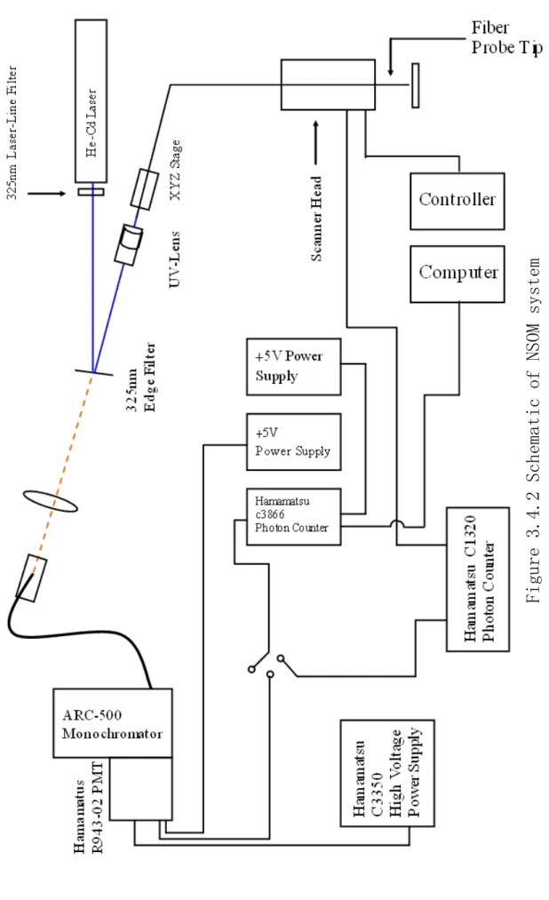
(25) 4. Fibers were dipped into BOE solution (HF: NH4F=1:6) for about 6-8 hours. (the. time depends on the ambient. temperature). 5. After etching completely, fibers were pulled out and dipped into ACE and D.I. water for rinse, respectively, and were blow-dried with N2 gas. 6. To avoid light leakage from the etched part of fiber, etched part of fiber is coated with Au by ion sputter (Hitachi E-1010) for 240sec(~50nm). Then, the fiber probe tip with metal coating is adhered to the one side of tuning fork (32.768 KHz) as shown in Figure 3.4.1. II. Experimental setup The scanning measurement was performed with Solver SNOM (Olympus based) developed at NT-MDT. As shown in Figure 3.4.2, He-Cd laser (325nm) was reflected from edge filter, coupled to the multimode fiber and illuminated the sample through the chemically etched tip. The resulting photoluminescence signals were collected by the same fiber (so called as I–C mode), passed. through. the. edge. filter,. 18. dispersed. by. ARC-500.
(26) monochromator, and detected by Hamamatsu R493-02 PMT. The signals from PMT were processed by Hamamatsu C3866 photon counter in all PL spectra measurements, while the PMT signals were amplified by Hamamatsu C1230 photon counter and processed using the controller of Solver SNOM when mapping the PL image.. 19.
(27) (a). (b). (C). 10μm. (d). (e). Figure 3.4.1 (a) Schematic representation of NSOM probe, (b) the non-coating probe tip in optical micrograph, (c) the probe tip with metal coating in optical micrograph, (d) and (e) are the SEM images of the coating tip.. 20.
(28) 21. Figure 3.4.2 Schematic of NSOM system.
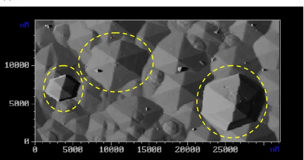
(29) 4 Results and Discussion 4.1 Surface Morphology of AlGaN Films The morphology of the two AlGaN films in this work is very different. AFM studies showed the surface with hexagonal hillocks in Sample A (Figure 4.1.1), while V-defects and cracks were observed on the surface of Sample B (Figure 4.1.2). According to the hexagonal hillock shapes in Sample A (Figure 4.1.1), they can be categorized into three groups: pyramid-like, mesa-like, and tent-like hillocks. Optical micrographs showed that most of the hillocks are pyramid-like and tent-like hillocks are sparser than others. For pyramid-like hillocks, their low-tilt inclined faces (with angle ranged from 2.5° to 13.0° between facets and plain region) are smooth extending from edge to an apex (Figure 4.1.3). For mesa-like hillocks, their slopes terminate on a quasi-flat facet that includes an angle smaller than 5° with respect to the plain surface. This looks like a truncated-pyramid at the angle of ~55° between the sidewalls and plain region (Figure 4.1.4), so is called mesa-like hillock. The geometric dimension. 22.
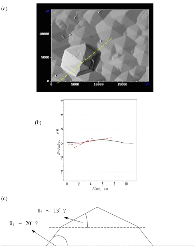
(30) distribution of mesa-like hillocks is typically 2-4 μm in width and 400-600 nm in height. Instead of continuous inclined faces as the pyramid-like hillock, the tent-like hillock consists of two-step inclined faces with different slopes, rising to an apex (Figure 4.1.5). The diameter of tent-like hillocks is about 5-10 μm, and its height is around 1 μm. The growth mechanisms of different types of hillocks have been discussed by several groups and were usually attributed to the strain relaxation or reduction of surface formation energy [16], [17]. [15],. .. In contrast, the hollow structures in Sample B looks like reversed hexagonal pyramids and are faceted as a V-shape (Figure 4.1.6 and Figure 4.1.7), so is named V-shape pit. The lateral size is about 0.5-3.0 μm. The hollow pit grows in the form of a six-walled structure with {110-1} surfaces. H. K. Cho et al. pointed out that the formation of V-shape pit originates from threading dislocation or stacking fault underneath. [18]. .. The formation mechanism of two kinds of microstructures, sinking V-pits or uprising hillocks, was ascribed to the strain. 23.
(31) relaxation. In Sample A, the smaller lattice constant a of AlN buffer layer (which is 3.1130 Å when fully relaxed. [13]. ) makes. the AlGaN film compressively stressed. In contrast, the larger lattice constant a of GaN buffer layer (3.1893 Å) in Sample B causes the AlGaN epitaxial layer under tensile strain. In the following sections, we will discuss the NSOM measurements of hillocks and V-defect in AlGaN films, respectively.. 24.
(32) (a). (b). Figure 4.1.1 (a) 2-D view, and (b) 3-D oblique view of Sample A probed by AFM. 25.
(33) Crack. 2μm. V-shaped pit. Figure 4.1.2 AFM 2-D image of Sample B. 26.
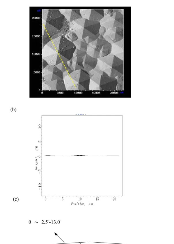
(34) (a). (b). (c). θ ~ 2.5°-13.0°. Figure 4.1.3 (a) AFM image, (b) the cross-sectional profile along dashed line, and (c) schematic draw of pyramid-like hillocks. 27.
(35) (a). (b). (c) θ2 ≦ 5° θ1 ~ 50°-60°. Figure 4.1.4 (a) AFM image, (b) the cross-sectional profile along dashed line, and (c) schematic draw of mesa-like hillocks. 28.
(36) (a). (b). (c) θ2 ~ 13° ? θ1 ~ 20° ?. Figure 4.1.5 (a) AFM image, (b) the cross-sectional profile along dashed line, and (c) schematic draw of tent-like hillocks. 29.
(37) Figure 4.1.6 AFM image of V-defect. 803 nm 385 nm. Figure 4.1.7 Cross-sectional profile of V-defect. 30.
(38) 4.2 Optical Properties of Hillocks In this section, we will analyze the optical properties of pyramid-like, mesa-like, tent-like hillocks, respectively, from NSOM measurements. I. Pyramid-like hillocks The NSOM morphological image of AlGaN film, Sample A, is shown in Figure 4.2.1. We observed one whole pyramid-like hillock Ⅰ, at the center of the image. Its lateral size is about 6μm with 1μm height. We took the NSOM PL spectra from different regions along the line crossing the slope and the apex (Figure 4.2.1(b)) of this pyramid-like hillock Ⅰ, as shown in Figure 4.2.1(c). The peak energy at the apex is 3.601 eV and is gradually blue-shifted to 3.650 eV when the probed spot is moved from the apex to the edge. In our previous studies. [1], [2]. ,. -1. Raman E2 (TO) mode displays a shift of less than 1 cm between the different regions of the surface consisting of many pyramid-like hillocks that is almost plain in optical micrographs. However, the Al content ranges from 12 % to 16 % from EDX measurements. Thus, it is likely that the obvious shift. 31.
(39) of the peak energy in NSOM PL spectra is due to Al composition gradient. The AlGaN energy gap dependence on Al content can be expressed as the following Al x Ga(1− x ) N. Eg. [13]. :. = (1 − x) ⋅ E gGaN + x ⋅ E gAlN − b ⋅ x ⋅ (1 − x) ,. where E gGaN (3.45 eV), E gAlN (6.13 eV) are the band gap of GaN and AlN, respectively, and b is the bowing parameter (1.3 eV). We obtain that Al content is 10.0 % at the apex and gradually increases to 12.9 % at the edge (See Figure 4.2.2). Figure 4.2.3 shows the NSOM intensity images at four different wavelengths, 338 nm (3.669 eV), 342 nm (3.626 eV), 344 nm (3.605 eV), and 346 nm (3.584 eV). The main features revealed from NSOM intensity images are as follows: (1) The edge of the hillock and the plain region appeared bright when probed at 338 nm (3.669eV) as compared to the hillocks, in agreement with the high Al content corresponding to the edge and surrounding region of the hillock. (2) The emission at 346 nm (3.584 eV) is correlated with pyramid-like hillock Ⅰ; The apex is brighter than surrounding regions, which may be due to the localization effect of band gap. (3) It can be seen clearly in. 32.
(40) the intensity plot that hillocks with different heights also show good contrast in comparison with the plain surface at different wavelengths. For instance, the emission at 342 nm (3.626 eV) is mainly from the lower hillocks at right hand of the image. It indicates that the peak energy of hillocks may be correlated to their heights and the Al composition at the apex of the lower hillock may be more than that of the higher one. As can seen in Figure 4.2.4, pyramid-like hillock Ι presents a strong intensity at 346 nm (3.584 eV).However, the maximum intensity when probing at 342 nm (3.626 eV) is from the hillock at the right hand of the cross-sectional profile, and the strong emissions for 338 nm (3.669 eV) are observed over the surrounding area. In Figure 4.2.5, we picked another hillock, pyramid-like hillock Ⅱ, with similar width as pyramid-like hillock Ι but with lower height only 450 nm. We observed the peak energy and Al content gradually increase from the apex to the edge (Figure 4.2.6). However, the peak energy at the apex of pyramid-like hillock Ⅱ (3.637 eV) is still higher than that of pyramid-like. 33.
(41) hillock Ι (3.601 eV). This difference supports that the peak energy may be related to the height. Figure 4.2.7 (a) shows the relationship between the peak energy at the apex and hillock height. The peak energy decreases from 3.639 eV to 3.593 eV as the height is increased from 450 nm to 1000 nm. It might be ascribed to inhomogeneous Al concentration as the apex of the hillock was formed. Figure 4.2.7 (b) shows the angle of the slope to the plain surface increases with the increasing height of pyramid-like hillocks. Thus, the Al concentration is also a function of the angle of the slope (see Figure 4.2.7 (c)). The relationship between the angle of the slope, the height of the hillock, and Al content at the apex may be ascribed to the stain relaxation. The relaxation of the elastic misfit strain, which is larger at the interface between the thin film and nucleation layer when the Al concentration is lower, caused a variation in orientation of the crystal plane. [19]. . Moreover, the. stress relaxation occurs via a transition from two-dimensional to three-dimensional growth mode, which may affect the growth rate in the normal direction. [20]. 34. ..
(42) (a). (c). 2μm. (b). Figure 4.2.1 (a) NSOM image, (b) cross-sectional profile, and (c) NSOM PL spectra of pyramid-like hillockⅠ. 35.
(43) (Edge) (Apex). (Edge). 3.70 15 3.68 14 3.66. Energy (eV). 3.64. 12. 3.62. 11 10. 3.60. Al concentration (%) calculated from NSOM PL. 13. 9 3.58 8 3.56 7 -6. -4. -2. 0. 2. 4. 6. Distance from the apex (µm). Figure 4.2.2 The peak energy and Al concentration profiles of pyramid-like hillock I. 36.
(44) 2μm. Figure 4.2.3 NSOM morphological image (16 μm × 7μm), NSOM intensity image at 346 nm (3.584 eV), 342 nm(3.605 eV), 344 nm (3.626 eV), and 338 nm (3.669 eV)of pyramid-like hillock Ⅰ. (The diagrams at right hand show the cross-sectional profiles of NSOM image.) 37.
(45) 1.4. 1.2. 346nm. 344nm. 0.8 342nm. 0.6. Height (µm). Intenesity(a.u.). 1.0. 338nm. 0.4. -2 0. 2. 4. 6. 0.2 8 10 12 14 16 18. Position (µm). Figure 4.2.4 The PL intensity at 338 nm (3.669 eV), 342 nm (3.626 eV), 344 nm (3.605 eV), and 346 nm (3.584 eV) as a function of the position along the slope of pyramid-like hillock Ⅰ. (The dash line shows the cross-section profile of pyramid-like hillock Ⅰ.) 38.
(46) (c) (a) 1μm. (b). Figure 4.2.5 (a) NSOM image, (b) cross-sectional profile, and (c) NSOM PL spectra of pyramid-like hillockⅡ.. 39.
(47) (Apex). (Edge). 3.70 3.68. Pyramid Ⅰ pyramid Ⅱ. 15. 3.66. Energy (eV). 13. 3.64. 12. 3.62. 11. 3.60. 10 9. 3.58. Al concentration (%) calculated from NSOM PL. 14. 8. 3.56 7. -1 0 1 2 3 4 Distance from the apex (µm). Figure 4.2.6 The peak energy and Al concentration profiles of pyramid-like hillock Ⅱ in comparison with pyramid-like hillock Ⅰ. 40.
(48) (a). (b). (c). Figure 4.2.7 (a) The peak energy and Al concentration at the apex of pyramid-like hillocks as a function of the angles, and (c) as a function of the heights. (b) The relationship between the angle of the slope respect to the plain surface and height of the pyramid-like hillocks heights. 41.
(49) II.. Mesa-like hillocks Figure 4.2.8 shows the optical micrograph of one mesa-like. hillock with 3 μm in width and the spectra corresponding to the center, edge , and surrounding area of the hillock. The micro-PL spectrum obtained at the surrounding area displays significant difference in comparison to the spectrum at the center. The INBE from the surrounding region peaks at 3.606 eV, while the center of the hillock displays much stronger IH at 3.559 eV. In our previous studies. [1], [2]. , the shift of energy peak. is attributed to the difference in Al content distribution (which is proved by EDX measurements). When the laser spot was focused on the hillock edge, we observed a wide emission band that might consists of INBE and IH. However, the spot size in our micro-PL system is about 2-3μm, so it is unlikely to get the correlation between luminescence and morphology of one mesa-like hillock in detail, especially for the steep slope with a width less than 300 nm. To get the better spatial resolution, we applied NSOM measurements (of which the resolution is less than 100 nm) to. 42.
(50) analyze the optical properties of different regions on one mesa-like hillock. Figure 4.2.9 shows another mesa-like hillock of ~3μm in width and ~0.8μm in height. The NSOM PL spectra were taken at the center, at the middle point between the center and the edge of the quasi-flat facet, on the slope and right on the edge of the mesa-like hillock. Not only the relative intensity but also the peak energy of the emission band differ from the probed regions. INBE band peaked at 3.623 eV was observed at the edge of the hillock, while the quasi-flat facet is dominated by IH (3.581 eV) and the intensity deceases rapidly form the center to the edge. In particular, the PL emission of the slope is dominated by the band peaked at 3.620 eV. It indicates the Al content at the slope may be 2.5 % more than that on the quasi-flat facet, as calculated from Vegard’s law. [13]. (see Figure 4.2.10). Lin et al. pointed out that the. hillocks nucleated form the nucleation layer in depth analysis of Raman measurement. [23]. . This suggested that at least two AlGaN. phases formed in the film nucleation process. By comparing the lattice misfit at the interface between the film and AlN. 43.
(51) nucleation layer when the thin film just started to form, the region with lower Al concentration suffers more compressive strain and that makes the island formation tend to be three-dimensional growth. So, the hillocks with lower Al concentration grow rapidly in normal direction, as the Al-rich region around grows more quickly in the lateral direction than in the normal direction. [20], [22]. . For mesa-like hillocks, the more. stress may be relaxed via a transition from two-dimensional to three-dimensional growth mode. Therefore the strain at the interface was released after the formation of the high island (the mesa-like hillock) and that is why Raman E2 (TO) mode is less on the mesa-like hillock than that on the plain region in Lin’s. measurements. [21]. .. Of. particular. concern. is. the. observation of the Al-rich slope, which is at the angle ~55 ° to the plain surface and that might be the characteristic of {1-101} facet. The growth-rate of {1-101} facet is much lower so that the growth of {1-101} facet is controlled partly by the kinetics on the surface. [23], [24]. . As a result, the {1-101} facet. may give rise to a local high Al content due to short diffusion. 44.
(52) length of Al atoms. In. intensity. mapping. images. (Figure. 4.2.11),. some. characteristics of the mesa-like hillock are observed: (1) The monochromatic plot at 346 nm (3.548 eV, the emission peak of IH) shows good contrast between the mesa-like hillock and the surrounding region. At the shorter probing wavelengths, the intensity deceases rapidly. It indicates IH is mainly from the quasi-flat region. (2) In the surrounding region, the luminescent intensity is stronger at 340 nm (3.647 eV) as compared with other longer probing wavelengths, which may be the evidence of higher peak energy and higher Al concentration in this region. (3) In particular, the luminescence at the slope is always weak at all the probing wavelengths, even though the probing wavelength is at 342 nm (3.626 eV, which is close to the emission peak energy in the PL spectra obtained from the slope). Figure 4.2.12 shows the intensity profile along the line crossing the surrounding region, the slope and the center of the mesa-like hillock. As expected, the quasi-flat facet. 45.
(53) displays a very high luminescence. The luminescent intensity from the center is about a factor of 7 higher than that from the edge of the hillock, which may be ascribed to the localization effect caused by Al-deficiency in the facet of the hillock. Vertical dashed lines indicate the slopes. The luminescence from the slopes is usually weak at all probing wavelengths. Even though the probing wavelength is at 342 nm (3.626 eV, which is close to the peak energy of the slope), the luminescence from the slopes is still weaker than other regions. We attributed the reduced luminescence efficiency to the point defects accumulated at the slope. S. Heikman et al. had pointed out that the increased n-type impurity incorporation on the {1-101} facet may be the origin of the point defects. 46. [24], [25], [26] ..
(54) Figure 4.2.8 Micro-PL spectra of one mesa-like hillock with 3 μm in width. 47.
(55) 2μm. Figure 4.2.9 NSOM image, cross-sectional profile, and NSOM PL spectra of one mesa-like hillock. (A, B, C, and D indicate the probed spots.) 48.
(56) Apex. Slope Edge. 3.64 12. Energy (eV). 11. 10. 3.60. 9 3.58. Al concentration (%) calculated from NSOM PL. 3.62. 8 3.56 7 0.0. 0.5. 1.0. 1.5. Distance from the center (µm). Figure 4.2.10 The peak energy and Al concentration profiles of mesas-like hillock. 49.
(57) 346 nm. 340 nm. 347 nm. 342 nm. 350 nm. 345 nm. 352 nm. Figure 4.2.11 NSOM morphological image (7 μm × 3μm) and NSOM intensity image at 340 nm (3.647 eV), 342 nm (3.626 eV),345 nm(3.594 eV), 346 nm(3.584 eV), 347 nm(3.573 eV), 350 nm (3.542 eV), and 352 nm (3.523 eV)of the mesa-like hillock. 50.
(58) 7. Height. 6 Height (µm). 5 4 3 2 1 0 0. 1. 2. 3 4 Position (µm). 5. 7. 7. 340 nm. 6. 6. 5. 5. Intensity (a.u.). Intensity (a.u.). 7. 6. 4 3 2 1 0. 1. 2. 3 4 Position (µm). 5. 7. 6. 3 2 1 0. 7. 1. 2. 3 4 Position (µm). 5. 7. 345 nm. 6. 6. 5. 5. Intensity (a.u.). Intensity (a.u.). 4. 0. 0. 4 3 2 1 0. 6. 7. 346 nm. 4 3 2 1 0. 0. 1. 2. 3 4 Position (µm). 5. 7. 6. 7. 0. 1. 2. 3 4 Position (µm). 5. 7. 347 nm. 6. 6. 5. 5. Intensity (a.u.). Intensity (a.u.). 342 nm. 4 3 2 1. 6. 7. 350 nm. 4 3 2 1 0. 0 0. 1. 2. 3 4 Position (µm). 5. 6. 7. 0. 1. 2. 3 4 Position (µm). 5. 6. 7. Figure 4.2.12 The height and PL intensity at 340 nm (3.647 eV), 342 nm (3.626 eV), 345 nm(3.594 eV), 346 nm(3.584 eV), 347 nm(3.573 eV),and 350 nm (3.542 eV) as a function of the position along the slope of the mesa-like hillock. 51.
(59) III. Tent-like hillocks Figure 4.2.13 shows the difference in micro-PL spectra between the tent-like hillock and the surrounding region. INBE (3.601 eV) was observed on the surrounding region while IH (3.546 eV) appeared at the apex. In our previous study. [2]. , the. obvious shift of the emission peak is mainly attributed to the Al. composition. fluctuation.. The. geometric. dimension. distribution of tent-like hillocks is typically 5- 10 μm in width. The micro-PL is capable of detecting the emission from the two different slopes of tent-like hillock. Lin et al. had pointed out that IH is resulted from the entire hillock. [23]. . As. we can see from NSOM-PL spectra in Figure 4.2.14 and Figure 4.2.15, the IH emission band is originated from different positions on the hillock and INBE is obtained from the edge and the surrounding region, no matter scanning from the apex to the edge along the ridgeline or the slope. The Al composition calculated from the Vegard’s law. [13]. indicated lower Al content. (~8.5 %) on the hillock in comparison with that (~12 %) from the. surrounding. region. (see. 52. Figure. 4.2.16).. The. Al.
(60) concentration is not so different between the ridge and the slope. However, in the intensity mapping images (Figure 4.2.17), we can obtain interesting behaviors corresponding to the morphology in detail: (1) The abrupt contrast is shown between the hillock and the surrounding region. When detecting at 340 nm (3.647 eV, the peak of INBE), the hexagonal dark region can be seen while the emission from the surrounding region is stronger. In contrast, when probing at 347 nm (3.573 eV, the peak of IH), the emission is mainly from the tent-like hillock. (2) In the intensity profiles shown in Figure 4.2.18, we observe that IH from the apex is stronger than INBE in the plain surface by a factor of 2, which is likely due to the localization effect caused by the fluctuation of Al content. Therefore, the carrier excited from the plain region would diffuse to the hillock, where Al content (band gap energy) is less. (3) The ridgeline gives brighter emission than the slope at 347 nm (IH). Table 4.2.1 gives comparisons between the apex, the ridgeline and the slope. From the relationship between intensity and full width at half maximum, we know that the emission efficiency is the. 53.
(61) best at the apex, fair at the ridge, and poor on the slope. In addition, the possibility for carriers to accumulate at the corner or the pointed end is larger than in a plain surface. This might explain why the intensity is stronger at the apex and the ridge is brighter than the slopes. By comparing three types of hillocks and plain surface, the peak energy at the apexes of all hillocks is smaller and the emission is stronger than those of the plain surface. Among the three types, the luminescent intensity from the pyramid-like hillock is the weakest, which may be ascribed to the localization effect so that the carrier on the plain region would easily diffused to the apex of hillock, which is the region with less Al content.. 54.
(62) Figure 4.2.13 Micro-PL spectra of one tent-like hillock with 6 μm in width. 55.
(63) 2 μm. Figure 4.2.14 (a) NSOM image, (b) cross-sectional profile along the ridgeline, and (c) NSOM PL spectra of the tent-like hillock. (A1, B1, C1, D1, E1, and F1 indicate the probed spot for PL.) 56.
(64) 2 μm. Figure 4.2.15 (a) NSOM image, (b) cross-sectional profile along the line crossing the slope and the apex, and (c) NSOM PL spectra of the tent-like hillock. (A2, B2, C2, D2, E2, and F2 indicate the probed spot for PL.) 57.
(65) (a) Along the ridgeline. 3.65 3.64. 12. Energy (eV). 3.62. 11. 3.61. Edge. Apex. 10. 3.60 3.59. 9. 3.58 3.57. 8. Al concentration (%) calculated from NSOM PL. 3.63. 3.56 -1. 0. 1. 2. 3. 4. 5. 6. Distance from the apex (µm). (b) Along the slope 3.64. Energy (eV). 3.62. 11. Edge. Apex. 10. 3.60. 9 3.58. Al concentration (%) calculated from NSOM PL. 12. 8 3.56. -1. 0. 1. 2. 3. 4 Distance from the apex (µm). 5. 6. Figure 4.2.16 The peak energy and Al concentration profiles along (a) the ridgeline and (b) the slope of the tent-like hillock. 58.
(66) Figure 4.2.17 NSOM morphological image (17 μm × 9μm) and NSOM intensity image at 339 nm (3.658 eV), 340 nm (3.647 eV), 341 nm (3.636 eV), 346nm (3.584eV), 347 nm(3.573 eV), and 348 nm(3.563 eV) of the tent-like hillock.. 59.
(67) Intensity (a.u.). 339 nm. 346 nm. 2.0. 2.0. 1.5. 1.5. 1.0. 1.0. 0.5. 0.5. 0.0 -2 0. 2. 4. 6. 0.0 -2 0. 8 10 12 14 16 18. 2. Position (µm). 4. 6. 8 10 12 14 16 18. Position (µm) 340 nm. 347 nm 2.0. Intensity (a.u.). 2.0. 1.5. 1.0. 0.5. 0.0 -2 0. 2. 4. 6. 1.5. 1.0. 0.5. 0.0 -2 0. 8 10 12 14 16 18. 2. Position (µm). 4. 6. 8 10 12 14 16 18. Position (µm) 341 nm. 348 nm. 2.0. 2.0. 1.5. 1.5. 1.0. 1.0. 0.5. 0.5. 0.0 -2 0. 2. 4. 6. 0.0 -2 0. 8 10 12 14 16 18. Position (µm). 2. 4. 6. 8 10 12 14 16 18. Position (µm). Figure 4.2.18 The PL intensity at 339 nm (3.658 eV), 340 nm (3.647 eV), 341 nm (3.636 eV), 346nm (3.584eV), 347 nm(3.573 eV), and 348 nm(3.563 eV) as a function of the position along the line indicated in Figure 4.2.17. The apex of the hillock is indicated by vertical dashed line.. 60.
(68) Position. Middle of. Middle of. ridgeline. slope. 2.0. 1.0. 0.8. 60±1. 67±2. 72±1. Apex. Intensity of IH (a.u.). FWHM of IH (eV). Table 4.2.1 The comparison between the apex, the slope, and the ridge of the tent-like hillock.. 61.
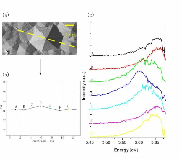
(69) 4-3 Optical properties of V-shape pit Figure 4.3.1 (a) shows one V-shape pit with 1μm in width and. 0.5 μm in depth. The NSOM PL spectra, scanned from the. edge to the center of the V-shape pit, reveal that the emission band (INBE) at ~3.70 eV appeared at all the probed points with no obvious shift. It indicates that the composition of Al is uniform that is in contrast with the result of A. Jimenez. [27]. .. They proposed that Al atoms would accumulate at the pits, and therefore Al composition was higher inside the pits. In addition, anther extra band Iv peaked at ~3.56. eV below the. band gap energy originated from the V-shape pit and the intensity of IV increased when moving close to the center of the pits (see Figure 4.3.1 (b)). In our previous study. [3]. , we. already suggested that IV band could be related to shallow acceptor levels, which is likely due to point defect of VGa. Figure 4.3.2 shows the near-field topographic image and monochromatic intensity-mapping. In the topographic image, we observed several pits about 0.5-2.0 μm in width and 0.2-1.0 μm in depth. In the image of IV, the emission is much stronger 62.
(70) inside the pits, and it is also clear that the intensity of IV is the highest at the center of the pit, which is stronger than IV from the edge by a factor of 7. It indicates that VGa are easily trapped at the pits, especially at the center of the pit. On the other hand, the emission of INBE shows no obvious contrast between flat region and pits, except for the perimeter of the pits. The emission intensity seems to be a little stronger around the edge of the pits. M.S. Jeong et al.. [28]. by. non-radiative. TEM. the. dislocations. (which. act. as. found that. recombination centers) moved toward to the pit, leaving a dislocation-free region around the pits, and hence the region around the pit edge seems to be the area with higher emission efficiency.. 63.
(71) 1 μm. Figure 4.3.1 the near-field topographic image and the NSOM PL spectra. (A, B, C and D indicate the probed points.) 64.
(72) (a). (b). (c). Figure 4.3.2 (a)The near-field topographic, (b)and (c) intensity mapping (~5 μm × 5 μm)taken at peak of IV and INBE, respectively. 65.
(73) 5 Conclusion In our previous study. [1]-[3]. , we already observed that the. extra red-shifted peak appeared both on the hillocks and inside the V-shape pit in comparison with the plain region on the AlGaN films by micro-PL. We suggested that the extra peak on the hillock was due to lower Al content while the additional peak inside the V-shape pit was attributed to Ga vacancy. However, the spatial resolution of micro-PL is ~ 3μm and the optical microscopy only reveals two-dimensional image of the sample surface. Therefore,. we have applied NSOM with higher spatial. resolution of ~100nm to investigate the correlation between the optical properties and the topography of single hillock or V-shape pit in this study. Special emphasis is put on the properties of pyramid-like hillocks (where seem to be the plain region under the optical microscopy of our micro-PL system), the steep slope of the mesa-like hillock, the difference between the apex, slope and ridge on the tent-like hillock and the properties of different regions of V-shape pit. For the pyramid-like hillocks, the peak energy increases. 66.
(74) from the apex to the edge of hillock. The emission peak energy at the apex of different hillocks decreases with the increasing height of hillock or the angle of the slope. We suggested the growth rate in the normal direction increased with the increasing strain caused by lattice misfit between the AlGaN thin film and AlN buffer layer when the film just start to form. For the mesa-like hillock, the emission (IH) from the slope is much weaker and the peak energy is higher than those of the quasi-flat facet. It may be due to the more Al content and high impurity density in the (1-101) facets. For the tent-like hillock, the emission peak did not shift among the various probed regions on the single hillock. Only the intensity showed difference. among. the. different. regions.. In. the. intensity-mapping, the apex is the brightest, and the intensity at the ridgeline is stronger than that from the slopes. As for the V-shape pit, the intensity of IV increased from the edge to the center.. This indicated the Ga vacancy easily. accumulated inside the pit, especially at the pit center.. 67.
(75) Reference [1] 陳蔚宗, 氮化鋁鎵薄膜表面 Hillock 缺陷之螢光研究 國立交通 大學 電子物理系所 碩士論文 2003 [2] 顏國錫, 氮化鋁鎵薄膜表面六角丘狀結構之研究 國立交通大學 電子物理系所 碩士論文 2004 [3] 彭瑞銘, 氮化鋁鎵 V 型缺陷之近場光學及掃瞄電位顯微鏡研究 國立交通大學 電子物理系所 碩士論文 2003 [4] O. Martinez et al, J. Appl. Phys., 96 3639 (2004) [5] R.Beye et al., Mat. Res. Soc. Proc., 499 113 (1997) [6] L.H. Robins, D.K. Wikenden , Appl. Phys. Lett,. 71 3841 (1997) [7] O.H. Nam et al., Mat. Res. Soc. Proc., 499 107 (1997) [8] W. Qian et al., Appl. Phys. Lett., 67 2284 (1995) [9] X.H. Wu et al., Appl. Phys. Lett., 72 682 (1998) [10]P.A. Crowell, D.K. Kim, and E.L. Hu, Appl. Phys. Lett., 72 927 (1998) [11]P. Chaudhari, J. Appl. Phys., 45 4339 (1974) [12]H. K. Cho et al., Appl. Phys. Lett. 79 215 (2001) [13]H. Angerer et al., Appl. Phys. Lett. 71 1504 (1997). 68.
(76) [14]W.R. Runyan and T.J. Shaffner, “Semiconductor Measurements and. Instrumentation”, second edition, The. McGraw-Hill companies, 1998 [15]S. Krramura et al., Jpn. J. Appl. Phys. 34 L1184 (1995) [16]K. Hiramatsu et al., Phys. Stat. Sol. (a) 176 535 (1999) [17]P. Charhari, J. Vac. Sci. Technol. 9 520 (1972) [18]H. K. Cho, J. Y. Lee and G. M. Yang, Appl. Phys. Lett. 80 1370 (2002) [19]M.Ohring, “The Material Science of Thin Films”, Academic Press, San Diego, 1992 [20]J. I. Pankove and T. D. Moustakas, “Gallium Nitride (GaN) Ⅱ”, Academic Press, San Diego, 1999 [21]林碧軒, 氮化鋁鎵薄膜表面六角丘狀結構螢光光譜及拉曼光譜 之研究 國立交通大學 電子物理系所 碩士論文. 2005. [22]R. Kröger et al., Appl. Phys. Lett. 97 083501 (2005) [23]T. Kato et al., Jpn. J. Appl. Phys. 42 1896 (2000) [24]S. Heikman et al., Jpn. J. Appl. Phys. 42 6276 (2003) [25]F. Bertram et al.,. Appl. Phys. Lett. 74 359 (1999). [26]K. Hiramatsu et al., Mater. Sci. Eng. 59 104 (1999). 69.
(77) [27]A. Jimenez et al., Mater. Sci. Eng B 93 64 (2002) [28]M. S. Jeong et al., Appl. Phys. Lett. 79 3440 (2001). 70.
(78)
數據
+7

相關文件
Particularly, combining the numerical results of the two papers, we may obtain such a conclusion that the merit function method based on ϕ p has a better a global convergence and
Then, it is easy to see that there are 9 problems for which the iterative numbers of the algorithm using ψ α,θ,p in the case of θ = 1 and p = 3 are less than the one of the
volume suppressed mass: (TeV) 2 /M P ∼ 10 −4 eV → mm range can be experimentally tested for any number of extra dimensions - Light U(1) gauge bosons: no derivative couplings. =>
For pedagogical purposes, let us start consideration from a simple one-dimensional (1D) system, where electrons are confined to a chain parallel to the x axis. As it is well known
The observed small neutrino masses strongly suggest the presence of super heavy Majorana neutrinos N. Out-of-thermal equilibrium processes may be easily realized around the
The temperature angular power spectrum of the primary CMB from Planck, showing a precise measurement of seven acoustic peaks, that are well fit by a simple six-parameter
incapable to extract any quantities from QCD, nor to tackle the most interesting physics, namely, the spontaneously chiral symmetry breaking and the color confinement..
(1) Determine a hypersurface on which matching condition is given.. (2) Determine a
