國 立 交 通 大 學
電信工程研究所
碩 士 論 文
制定饋入低剖面天線的標準流程圖及使用反射
相位萃取人造磁導體頻帶
Formulation of a Standard Flow Chart of Feeding the Low
Profile Antenna and Extraction of the Artificial Magnetic
Conductor Band from the Reflection Phases
研究生:黃建融 (Chien-Jung Huang)
指導教授:黃謀勤 博士 (Dr. Malcolm Ng Mou Kehn)
制定饋入低剖面天線的標準流程圖及使用反射相位萃取人
造磁導體頻帶
Formulation of a Standard Flow Chart of Feeding the Low
Profile Antenna and Extraction of the Artificial Magnetic
Conductor Band from the Reflection Phases
研 究 生:黃建融 Student:Chien-Jung Huang
指導教授:黃謀勤 Advisor:Malcolm Ng Mou Kehn
國 立 交 通 大 學
電信工程研究所
碩 士 論 文
A Thesis
Submitted to Institute of Computer and Information Science College of Electrical Engineering and Computer Science
National Chiao Tung University in partial Fulfillment of the Requirements
for the Degree of Master in
Communication Engineering
August 2013
Hsinchu, Taiwan, Republic of China
i
制定饋入低剖面天線的標準流程圖及使用反射相位萃取人造磁導體
頻帶
學生:黃建融
指導教授:黃謀勤 博士
國立交通大學電信工程研究所碩士班
摘
要
在設計低剖面天線時最常使用的方法就是將傳統天線和高阻抗平
面組合在一起,這是因為高阻抗平面可以模擬完美磁導體的特性,而
用以增加天線的輻射。但儘管如此,如何去饋入這樣的低剖面天線仍
然是一個很大的研究課題,這是因為高阻抗平面雖然擁有可以近似人
工磁導體的條件,但卻被頻率所限制。這代表高阻抗平面只能在特定
的頻率範圍內才能擁有完美磁導體的特性,而這個頻帶就稱為人工磁
導體頻帶。目前對於低剖面天線已經有了非常多且深入的研究資料,
但仍然沒有一個有系統的饋入方法。有鑑於此,制定一個具有可重複
性的系統方法去匹配低剖面天線就成為了我們想要達成的目的。
為了實現我們的想法,我們必須先了解反射相位,這是因為當我們
談論到高阻抗平面結構時,很多研究者會使用反射相位來描述它的人
工磁導體的頻帶,此頻帶位於反射相位±45°之間(其反射相位 0°具有
完美磁導體的特性)。儘管如此,這並沒有考慮到傳統天線的輻射場
型。由於一般在定義反射相位時,最常見的是使用垂直入射的電磁波
去測量,但在高阻抗平面上的傳統天線所發出之電磁波並非只有垂直
入射。因此,我們的首要任務就是去了解並分析傳統天線的場型,再
用以萃取人工磁導體頻帶。
ii
Formulate a Standard Flow Chart of Feeding the Low Profile Antenna
and Extract the AMC Band from the Reflection Phases
student:Chien-Jung Huang
Advisors:Dr. Malcolm Ng Mou Kehn
Institute of
Communications EngineeringNational Chiao Tung University
ABSTRACT
A popular way to design a low profile antenna is by combining the
traditional antenna with a high impedance surface (HIS), because the HIS
can mimic the property of the perfect magnetic conductor (PMC) to
improve the radiation. However, the way to feed the low profile antenna
is still a big issue because the artificial magnetic conductor (AMC)
condition of the HIS is a frequency-dependent property. It means the
frequency band in which the PMC property of the HIS prevails is limited.
This band is termed as the AMC region. There had been intensive
research performed on the low profile antenna but there has not been a
consistent, let alone identical method for feeding the low profile antenna.
In consideration of that, matching the low profile antenna by a systematic
way is our purpose.
To fulfill our idea, we should introduce the reflection phase first,
because when talking about the HIS structure, many researchers usually
characterize the AMC region of the HIS by the frequency range in which
the reflection phase lies between ±45° (0° of reflection phase pertains to
PMC property). However, this does not consider the radiation pattern of
the traditional antenna. Because the reflection phase of the general
definition is defined by the normal incident wave, the waves excited by
the traditional antenna on the HIS are not all normal incident waves
toward the HIS. Therefore surveying the pattern of the traditional antenna
becomes the priority to extract the AMC band.
iii
誌
謝
能夠完成這篇論文,首先要感謝的是我的指導教授 黃謀勤博士,
在經由他的指導與建議之下,使得我在研究的路途上能有一個明確的
方向。在他的鼓勵之下,還去參加了國際研討會(APMC),體驗了和國
際學者的交流與互動。
再來要感謝的是我實驗室的同學,菜埔和阿嘉,在這研究所的兩年,
我們一起修課、寫計劃書、做研究和實驗以及處理雜事,謝謝他們的
幫忙才能使我在研究所的生活如此順利。另外也十分感謝其他實驗室
的朋友們,在研究實驗及量測上提供了許多幫忙,特別感謝蔡宜哲博
班學長,給予我非常多的幫助。還有多虧南更、偉全、諸葛(釋伊夏)、
永勳(斬無私)的適時加入,讓實驗室增加了許多歡樂。
而我也十分感謝電信所上的老師們,從他們所開設的課上,我學習
到了很多的知識,如果我之後能在電信領域有一點點的貢獻,肯定都
是要歸功於他們的付出。
最後,我要謝謝在我背後支持及鼓勵我的家人及朋友,讓我在研究
所的這兩年,能夠有非常開心的生活,使我每天充滿動力,去迎接每
一天的挑戰。
iv
TABLE OF CONTENTS
CHINESE ABSTRACT………i ENGLISH ABSTRACT………ii ACKNOWLEDGEMENT………iii
TABLE OF CONTENTS …………
ivLIST OF FIGURES ……
………vi
Chapter 1 Introduction ... 1
1.1 Motivation ... 1
1.2 High impedance surface ... 2
1.3 Low profile antenna ... 3
1.4 Reflection phase ... 4
Chapter 2 Formulate a standard flow chart of feeding the low profile antenna ... 11
2.1 Design the standard flow chart of feeding the low profile antenna ... 11
2.2 The example of the low profile antenna composed of the corrugated surface and the half-wave dipole antenna ... 12
2.3 Verify the simulation result and the measurement result ... 20
Chapter 3 Extract the AMC region of the HIS from the radiation pattern of the traditional antenna and the reflection phases of the HIS ... 23
3.1 The radiation pattern of the traditional half-wave dipole antenna ... 23
3.2 The global definition of the reflection phase ... 25
3.3 Extract the AMC region of the HIS ... 26
3.4 Redesign the low profile antenna in Section 2.2 by the effective reflection phase ... 29
3.5 Verify the simulation result and the measurement result ... 35
v
4.1 Frequency selective surface (FSS) ... 38
4.2 Calculate the effective reflection phase according to the radiation pattern of the traditional antenna ... 39
4.3 Utilize the standard flow chart to design the low profile antenna ... 41
4.4 Verify the simulation result and the measurement result ... 48
Chapter 5 Apply to the different type of the traditional antenna ... 51
5.1 The structure and the radiation pattern of the traditional folded dipole antenna ... 51
5.2 Extract the AMC region of the FSS ... 52
5.3 Utilize the standard flow to design the low profile antenna ... 53
5.4 Verify the simulation result and the measurement result ... 60
Chapter 6 Conclusion ... 62
vi
LIST OF FIGURES
Figure 1.1 (a) The 𝐸𝑡 and 𝐻𝑡 on the PEC and their relationship. (b) The 𝐸𝑡 and 𝐻𝑡 on the PMC and their relationship. (c) The 𝐸𝑡 and 𝐻𝑡 on the HIS and their relationship. ... 3 Figure 1.2 (a) Image property of the PEC. (b) Image property of the PMC. ... 4 Figure 1.3 (a) The incident wave and the reflected wave on the PEC. (b) The
reflection phase of the PEC... 5 Figure 1.4 (a) The incident wave and the reflected wave on the PMC. (b) The
reflection phase of the PMC. ... 6 Figure 1.5 (a) The incident wave and the reflected wave on the HIS. (b) The reflection phase of the HIS. ... 7 Figure 1.6 (a) The first step of the refection phase measurement (b) The phase
difference of the surface under test including the space distance. ... 8 Figure 1.7 (a) The second step of the refection phase measurement (b) The phase difference of the metal including the space distance. ... 9 Figure 1.8 The third step of the reflection phase measurement (a) The phase difference of the surface under test including the space distance. (b) The phase difference of the metal including the space distance. (c) The reflection phase of the metal. (d) The reflection phase of the surface under test. ... 10 Figure 2.1 The standard design flow chart of the low profile antenna ... 11 Figure 2.2 The structure and the dimension of the corrugated surface. ... 13 Figure 2.3 The reflection phase of the corrugated surface and the 0° point is at 9.026 GHz. ... 13
vii
Figure 2.4 The dimension of the low profile antenna composed of the half-wave
dipole antenna and the corrugated surface. ... 14
Figure 2.5 Substitute the PMC for the corrugated surface... 15
Figure 2.6 The impedance of the low profile antenna composed of the PMC. ... 15
Figure 2.7 The dimension of the RO4003 printed circuit board. ... 16
Figure 2.8 The structure and the dimension of the balun made by the RO4003. ... 17
Figure 2.9 The impedance of the low profile antenna with the balun. ... 17
Figure 2.10 The structure and the dimension of the transformer to the 50 ohms transmission line. ... 18
Figure 2.11 The return loss of the low profile antenna including the feeding network with the PMC. ... 19
Figure 2.12 Substitute the corrugated surface for the PMC back. ... 19
Figure 2.13 The return loss of the low profile antenna including the feeding network with the corrugated surface. ... 20
Figure 2.14 (a)The fabrication of the corrugated surface. (b) Its reflection phase. ... 21
Figure 2.15 (a)The fabrication of the feeding network. (b) The measurement situation of the low profile antenna. ... 22
Figure 2.16 The return loss of the low profile antenna. ... 22
Figure 3.1 (a) The 3D pattern of the half-wave dipole antenna. (b) The yz plane pattern. ... 24
Figure 3.2 The waves exited by the half-wave dipole antenna illuminate the HIS with different angles and strengths. ... 24
Figure 3.3 (a) The 𝑇𝐸𝜃 definition of the reflection phase. (b) The 𝑇𝑀𝜃 definition of the reflection phase. ... 25
viii
Figure 3.4 (a) The measurement method of the global reflection phase. (b) Three examples of the 𝑇𝐸𝜃 mode. ... 26 Figure 3.5 The 𝑇𝐸𝜃 mode waves excited by the half-wave dipole antenna on the corrugated surface. ... 27 Figure 3.6 The reflection phases of the corrugated surface. ... 27 Figure 3.7 The effective reflection phases of the corrugated surface. ... 29 Figure 3.8 The corrugated surface’s effective reflection phase is 0° at 9.945 GHz. . 30 Figure 3.9 The impedance of the low profile antenna composed of the PMC. ... 31 Figure 3.10 The structure and the dimension of the balun made by the RO4003. ... 32 Figure 3.11 The impedance of the low profile antenna with the balun. ... 32 Figure 3.12 The structure and the dimension of the transformer to the 50 ohms
transmission line. ... 33 Figure 3.13 The return loss of the low profile antenna including the feeding network with the PMC. ... 34 Figure 3.14 Substitute the corrugated surface for the PMC back. ... 34 Figure 3.15 The return loss of the low profile antenna including the feeding network with the corrugated surface. ... 35 Figure 3.16 The fabrication of the corrugated surface’s global reflection phase
examples. ... 36 Figure 3.17 (a)The fabrication of the feeding network. (b) The measurement situation of the low profile antenna. ... 37 Figure 3.18 The return loss of the low profile antenna. ... 37 Figure 4.1 The structure and the dimension of the FSS. ... 39 Figure 4.2 (a) The reflection phases of the FSS. (b) The FSS’ effective reflection
ix
phase is 0° at 8.44 GHz. ... 40
Figure 4.3 The dimension of the low profile antenna composed of the half-wave dipole antenna and the FSS. ... 41
Figure 4.4 Substitute the PMC for the FSS... 42
Figure 4.5 The impedance of the low profile antenna composed of the PMC. ... 43
Figure 4.6 The structure and the dimension of the balun made by the RO4003. ... 44
Figure 4.7 The impedance of the low profile antenna with the balun. ... 45
Figure 4.8 The structure and the dimension of the transformer to the 50 ohms transmission line. ... 46
Figure 4.9 The return loss of the low profile antenna including the feeding network with the PMC. ... 46
Figure 4.10 Substitute the FSS for the PMC back. ... 47
Figure 4.11 The return loss of the low profile antenna including the feeding network with the FSS. ... 48
Figure 4.12 (a)The fabrication of the FSS. (b) Its reflection phases. ... 49
Figure 4.13 (a)The fabrication of the feeding network. (b) The measurement situation of the low profile antenna. ... 50
Figure 4.14 The return loss of the low profile antenna. ... 50
Figure 5.1 The shape of the folded dipole antenna. ... 51
Figure 5.2 (a) The 3D pattern of the folded half-wave dipole antenna. (b) The yz plane pattern. ... 52
Figure 5.3 The 𝑇𝐸𝜃 mode waves excited by the folded dipole antenna on the FSS. 53 Figure 5.4 The dimension of the low profile antenna composed of the folded half-wave dipole antenna and the FSS. ... 54
x
Figure 5.5 Substitute the PMC for the FSS... 54
Figure 5.6 The impedance of the low profile antenna composed of the PMC. ... 55
Figure 5.7 The structure and the dimension of the balun made by the RO4003. ... 56
Figure 5.8 The impedance of the low profile antenna with the balun. ... 57
Figure 5.9 The structure and the dimension of the transformer to the 50 ohms transmission line. ... 58
Figure 5.10 The return loss of the low profile antenna including the feeding network with the PMC. ... 58
Figure 5.11 Substitute the FSS for the PMC back. ... 59
Figure 5.12 The return loss of the low profile antenna including the feeding network with the FSS. ... 59
Figure 5.13 (a)The fabrication of the feeding network. (b) The measurement situation of the low profile antenna. ... 61
1
Chapter 1 Introduction
1.1 Motivation
It has become increasingly important to use many antennas of different kinds for various purposes ever since the explosive growth of wireless communications technology. There are many applications such as mobile phones, vehicular
communications, digital house systems, and so on. Typically, compact planar antennas are required. For most applications, it is important for planar antennas to be also low profile [1]–[3], so that they can be applied to vehicles and digital houses with minimal protrusion due to their thin thicknesses. A popular way to design a low profile antenna is by combining the traditional antenna with a high impedance surface (HIS) [3]–[9], because the HIS can mimic the property of the perfect magnetic conductor (PMC) to improve the radiation. However, the way to feed the antenna is still a big issue because the artificial magnetic conductor (AMC) [2, 10] condition of the HIS is a frequency-dependent property. It means the frequency band in which the PMC
property of the HIS prevails is limited. This band is termed as the AMC region. There had been intensive research performed on the low profile antenna but there has not been a consistent, let alone identical method [3, 9] for feeding the antenna. In consideration of that, matching the low profile antenna by a systematic way is our purpose since the antenna has good radiation property only if the feeding power can be transmitted to the antenna. Therefore a systematic method for feeding the low profile antenna is first sought. The design procedure includes three parts: first, simulate the traditional antenna on the PMC to find out the impedance of the low profile antenna; second, design the feeding network circuit to match the low profile
2
antenna; third, use the HIS to substitute for the PMC and get good agreement with our expectation. To fulfill our idea, we should introduce the reflection phase [1, 11] first, because when talking about the HIS structure, many researchers usually characterize the AMC region of the HIS by the frequency range in which the reflection phase lies between ±45° [3, 6] (0° of reflection phase pertains to PMC property). The design procedure developed in this thesis is systematic and general.
1.2 High impedance surface
Before introducing the HIS, we should introduce the two ideal physical entities used in electromagnetic theory. One of them is the perfect electric conductor (PEC), over which the surface tangential electric field (𝐸⃑⃑⃑ ) vanishes, whereas the tangential 𝑡
magnetic field (𝐻⃑⃑⃑⃑ ) must not be zero. As the |𝐸𝑡 ⃑⃑⃑ | divided by the |𝐻𝑡 ⃑⃑⃑⃑ | equals to zero, 𝑡 the PEC is a zero impedance surface, as shown in Figure 1.1 (a). The other is the perfect magnetic conductor (PMC), whose tangential electric field 𝐸⃑⃑⃑ on the surface 𝑡
must not be zero, whereas the 𝐻⃑⃑⃑⃑ must be vanish. For this case, the |𝐸𝑡 ⃑⃑⃑ | divided by 𝑡 the |𝐻⃑⃑⃑⃑ | is infinity, so the PMC is an infinite impedance surface, as shown in Figure 𝑡 1.1 (b). The so-called HIS bears the property whereby the 𝐸⃑⃑⃑ on the surface is not 𝑡 zero, and the 𝐻⃑⃑⃑⃑ is very small. In this way, the |𝐸𝑡 ⃑⃑⃑ | divided by the |𝐻𝑡 ⃑⃑⃑⃑ | is a very 𝑡 high value, such that the HIS is regarded as a high impedance surface, as shown in Figure 1.1 (c).
3
1.3 Low profile antenna
According to the image theory, the electric current source can be mirrored about the surfaces of both the electric and magnetic conductors but they have different
directions as shown in Figure 1.2. To achieve the concept of the low profile antenna, the distance between the radiation source and the conductor ground plane should be very small and the radiation source should be horizontal. Therefore, if the electric conductor is used as the ground plane, the radiation source of the electric current will be canceled by the image theory. As such, these points to the use of a magnetic conducting ground plane instead of an electric conducting one for achieving low
(c)
𝐸
𝑡⃑⃑⃑
𝐻
⃑⃑⃑⃑
𝑡|𝐸
⃑⃑⃑ |
𝑡|𝐻
⃑⃑⃑⃑ |
𝑡= 0
Figure 1.1 (a) The 𝐸⃑⃑⃑ and 𝐻𝑡 ⃑⃑⃑⃑ on the PEC and their relationship. (b) The 𝐸𝑡 ⃑⃑⃑ and 𝑡
𝐻𝑡
⃑⃑⃑⃑ on the PMC and their relationship. (c) The 𝐸⃑⃑⃑ and 𝐻𝑡 ⃑⃑⃑⃑ on the HIS and their 𝑡
relationship.
PEC
𝐸
𝑡⃑⃑⃑
𝐻
𝑡⃑⃑⃑⃑
|𝐸
⃑⃑⃑ |
𝑡|𝐻
⃑⃑⃑⃑ |
𝑡→ ∞
PMC
𝐸
𝑡⃑⃑⃑
𝐻
𝑡⃑⃑⃑⃑
|𝐸
⃑⃑⃑ |
𝑡|𝐻
⃑⃑⃑⃑ |
𝑡→ ℎ𝑖𝑔ℎ 𝑣𝑎𝑙𝑢𝑒
HIS
(a) (b)4
profile antennas.
In the natural world, the Earth contains an abundance of the good electric conductors, whereas good magnetic conductors do not naturally occur at all. The HIS is one of the substitutes for the magnetic conductor. Unfortunately, though the HIS can mimic the magnetic conductor, it is frequency-dependent. Unlike the wideband nature of the natural electric conductor, the HIS has a limited band to mimic the good magnetic conductor. Consequently, there are still many challenges to apply the HIS, and one of the challenges is to find out where the good magnetic conductor band is.
Generally there is one method to find out where the good magnetic conductor band is by interpreting the reflection phase. When looking up the literatures, using the
reflection phase to describe the AMC band and then design the low profile antenna is popular.
1.4 Reflection phase
General definition: suppose there is a periodic structure which is extended infinitely, and now emit a plane wave to this periodic structure normally, and then determine the electric field phase difference of the incident wave and the reflected wave. The phase
Copied sources
h
h
PEC
Electric Electric Magnetic Magnetic
Actual sources
Copied sources h
h
PMC
Electric Electric Magnetic Magnetic
Actual sources
(a) (b)
5
difference is the reflection phase of this periodic structure. Generally, the reflection phase of an ideal PEC structure is always 180° as shown in Figure 1.3. Otherwise, the reflection phase of an ideal PMC structure is always 0° as shown in Figure 1.4. Both of them do not vary with the frequency.
𝐸
𝑜𝑢𝑡⃑⃑⃑⃑⃑⃑⃑⃑
𝑘
𝑜𝑢𝑡⃑⃑⃑⃑⃑⃑⃑⃑
𝑘
𝑖𝑛⃑⃑⃑⃑⃑
𝐸
𝑖𝑛⃑⃑⃑⃑⃑
𝐻
⃑⃑⃑⃑⃑⃑
𝑖𝑛PEC
𝐻
𝑜𝑢𝑡⃑⃑⃑⃑⃑⃑⃑⃑⃑
(a) 0 2 4 6 8 10 12 14 16 18 20 -200 -150 -100 -50 0 50 100 150 200 Frequency (GHz) Refl ect io n Ph as e (d eg ree) (b)Figure 1.3 (a) The incident wave and the reflected wave on the PEC. (b) The reflection phase of the PEC.
6
In the natural world, the property of metals can be similar to that of the PEC, so when we need to use the PEC, we will substitute the metal for the PEC. However, we cannot find materials that are similar to the PMC in the natural world. To fulfill the desire of the PMC, there comes a method which is the HIS concept. We use the property of the periodic structure, and it can reach 0° of the reflection phase as shown in Figure 1.5. The reflection phase can be 0° by the property of the HIS, but the phase will vary with the frequency. Therefore, how to apply HIS to be similar to
𝐻
𝑜𝑢𝑡⃑⃑⃑⃑⃑⃑⃑⃑⃑
𝑘
𝑜𝑢𝑡⃑⃑⃑⃑⃑⃑⃑⃑
𝑘
𝑖𝑛⃑⃑⃑⃑⃑
𝐻
𝑖𝑛⃑⃑⃑⃑⃑⃑
𝐸
⃑⃑⃑⃑⃑
𝑖𝑛PMC
𝐸
𝑜𝑢𝑡⃑⃑⃑⃑⃑⃑⃑⃑
(a) (b)Figure 1.4 (a) The incident wave and the reflected wave on the PMC. (b) The reflection phase of the PMC.
0 2 4 6 8 10 12 14 16 18 20 -200 -150 -100 -50 0 50 100 150 200 Frequency (GHz)
Refl
ect
io
n
Ph
as
e
(d
eg
ree)
7
the PMC becomes the research topic nowadays.
Measurement: because there is no equipment which can determine the phase
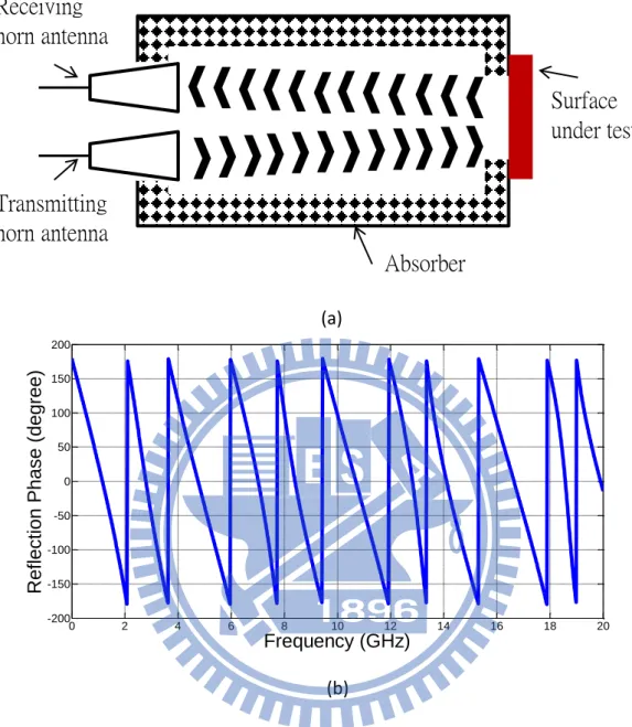
difference directly on the surface under test when the plane wave hits the surface, we should utilize the following three steps to obtain the reflection phase.
First step is to use the horn antenna to emit the wave. At a sufficiently large distance away, the wave can be similar to the plane wave. After this plane wave hits the surface under test, use the other horn antenna to receive the reflected wave, and then obtain the phase difference including the space distance as shown in Figure 1.6.
𝐸
𝑜𝑢𝑡⃑⃑⃑⃑⃑⃑⃑⃑
𝑘
𝑜𝑢𝑡⃑⃑⃑⃑⃑⃑⃑⃑
𝑘
𝑖𝑛⃑⃑⃑⃑⃑
𝐸
𝑖𝑛⃑⃑⃑⃑⃑
𝐻
⃑⃑⃑⃑⃑⃑
𝑖𝑛HIS
𝐻
𝑜𝑢𝑡⃑⃑⃑⃑⃑⃑⃑⃑⃑
(a) (b)Figure 1.5 (a) The incident wave and the reflected wave on the HIS. (b) The reflection phase of the HIS.
0 2 4 6 8 10 12 14 16 18 20 -200 -150 -100 -50 0 50 100 150 200 Frequency (GHz) Reflection Phase (de gree)
8
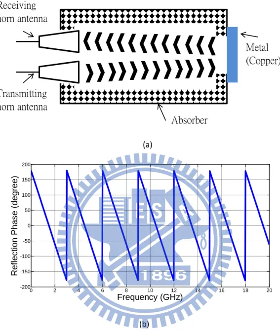
Second step is to substitute the metal for the surface under test. Then process the first step where we use the horn antenna to obtain the phase difference as shown in Figure 1.7. The significance of this step is that we calibrate the phase difference of the space distance between the horn antenna and the surface under test by it.
(a)
Surface
under test
Transmitting
horn antenna
Receiving
horn antenna
Absorber
0 2 4 6 8 10 12 14 16 18 20 -200 -150 -100 -50 0 50 100 150 200 Frequency (GHz) Reflection Phase (de gree) (b)Figure 1.6 (a) The first step of the refection phase measurement (b) The phase difference of the surface under test including the space distance.
9
Third step is to subtract the phase difference of the metal including the space distance from the phase difference of the surface under test including the space distance and add the metal reflection phase which is 180°. Then after limiting the phase between 180° and −180°, the final data is the reflection phase of this surface under test as shown in Figure 1.8. (a)
Metal
(Copper)
Transmitting
horn antenna
Receiving
horn antenna
Absorber
0 2 4 6 8 10 12 14 16 18 20 -200 -150 -100 -50 0 50 100 150 200 Frequency (GHz) Reflection Phase (de gree) (b)Figure 1.7 (a) The second step of the refection phase measurement (b) The phase difference of the metal including the space distance.
10 (b) 0 2 4 6 8 10 12 14 16 18 20 -200 -150 -100 -50 0 50 100 150 200 Frequency (GHz) Reflection Phase (de gree) 0 2 4 6 8 10 12 14 16 18 20 -200 -150 -100 -50 0 50 100 150 200 Frequency (GHz) Reflection Phase (de gree) 0 2 4 6 8 10 12 14 16 18 20 -200 -150 -100 -50 0 50 100 150 200 Frequency (GHz) Refl ect ion Ph ase (d eg ree) 0 2 4 6 8 10 12 14 16 18 20 -200 -150 -100 -50 0 50 100 150 200 Frequency (GHz) Reflection Phase (de gree) (a) (c) (d)
Figure 1.8 The third step of the reflection phase measurement (a) The phase difference of the surface under test including the space distance. (b) The phase difference of the metal including the space distance. (c) The reflection phase of the metal. (d) The reflection phase of the surface under test.
11
Chapter 2 Formulate a standard flow chart of
feeding the low profile antenna
2.1 Design the standard flow chart of feeding the low
profile antenna
Recently there are more and more researches of the low profile antenna, but there is still no systematic method about how to feed the low profile antenna. Therefore there are many different feeding methods when using the different types of the HIS
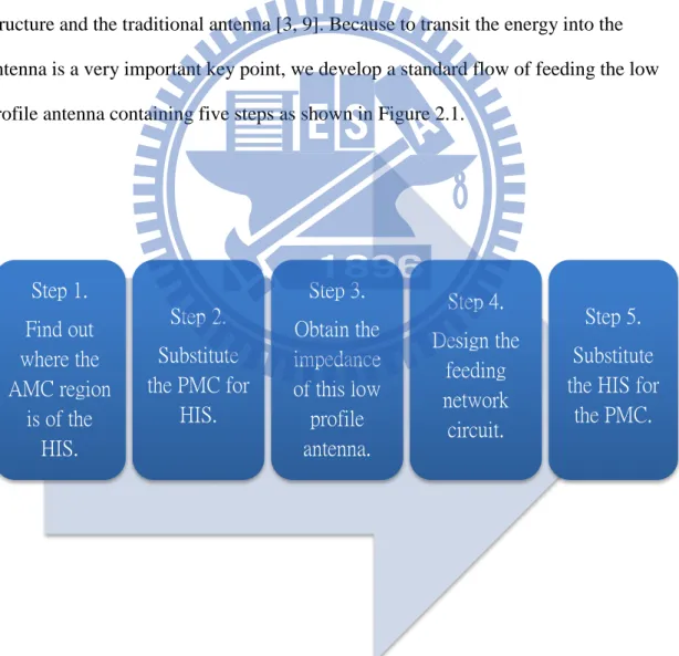
structure and the traditional antenna [3, 9]. Because to transit the energy into the antenna is a very important key point, we develop a standard flow of feeding the low profile antenna containing five steps as shown in Figure 2.1.
Step 1, find out where the AMC region is of the HIS: utilize the reflection phase to
Step 1. Find out where the AMC region is of the HIS. Step 2. Substitute the PMC for HIS. Step 3. Obtain the impedance of this low profile antenna. Step 4. Design the feeding network circuit. Step 5. Substitute the HIS for
the PMC.
12
find out the AMC region of the HIS, and in this region the HIS will have the approximate property of the PMC.
Step 2, Substitute the PMC for HIS: because the low profile antenna is composed of the traditional antenna and the HIS, if the operating frequency is in the AMC region of the HIS, we can substitute the PMC with HIS when simulating by computer.
Step 3, obtain the impedance of this low profile antenna: we can get the input impedance of this low profile antenna in the Smith chart by the simulation software. Step 4, design the feeding network circuit: use the matching circuit to adjust the input impedance to near 50 ohms, and then it will own the good return loss we want. Step5, Substitute back the HIS for the PMC: change back the HIS again, and then confirm whether the simulations of the PMC case and the HIS case have the good agreement with the approximate return loss or not.
2.2 The example of the low profile antenna composed
of the corrugated surface and the half-wave dipole
antenna
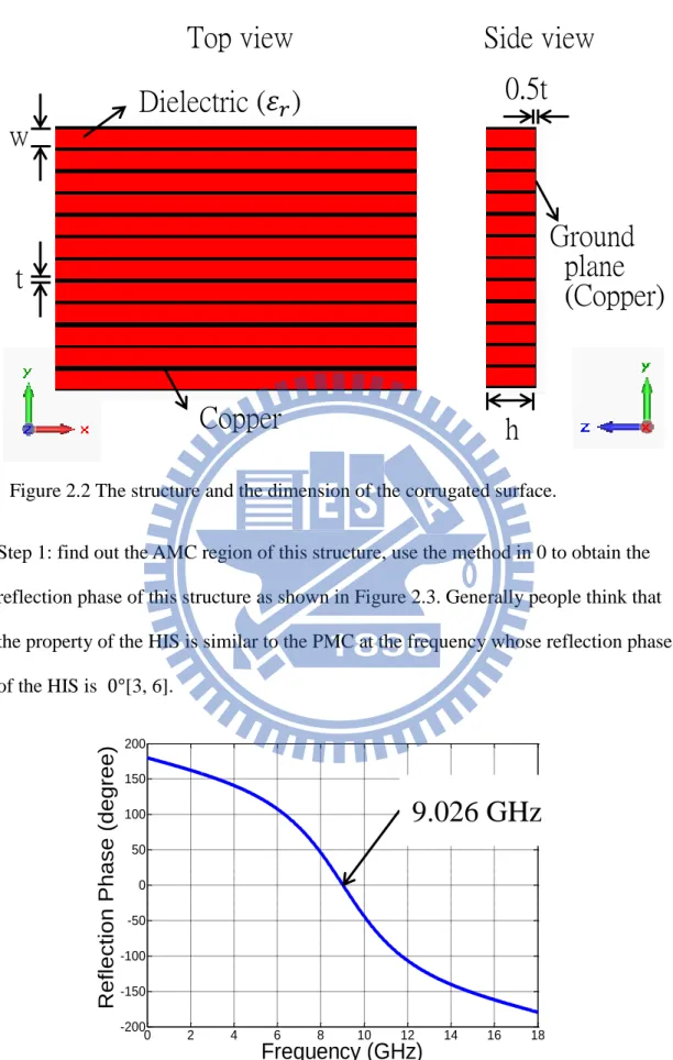
At first we use an example to experiment, and we will make use of the corrugated surface as the HIS in this example as shown in Figure 2.2, and the parameter are
w = 1.5 mm, t = 0.2 mm, h = 4 mm, 𝜀𝑟 = 4.3,
13
Step 1: find out the AMC region of this structure, use the method in 0 to obtain the reflection phase of this structure as shown in Figure 2.3. Generally people think that the property of the HIS is similar to the PMC at the frequency whose reflection phase of the HIS is 0°[3, 6].
Ground
plane
(Copper)
Copper
Dielectric (𝜀
𝑟)
Side view
0.5t
h
w
t
Top view
Figure 2.2 The structure and the dimension of the corrugated surface.
0 2 4 6 8 10 12 14 16 18 -200 -150 -100 -50 0 50 100 150 200
Frequency (GHz)
Reflection Phase (degree)9.026 GHz
Figure 2.3 The reflection phase of the corrugated surface and the 0° point is at 9.026 GHz.
14
Then we judge the frequency whose reflection phase is 0° is the same frequency that we will design and operate the low profile antenna at the frequency. Due to Figure 2.3 we know the frequency is 9.026 GHz. Because the half-wave dipole antenna has well-known good radiation behavior, in this example we will combine the low profile antenna with the half-wave dipole antenna operating near 9.026 GHz and the
corrugated surface as shown in Figure 2.4, and its parameters are
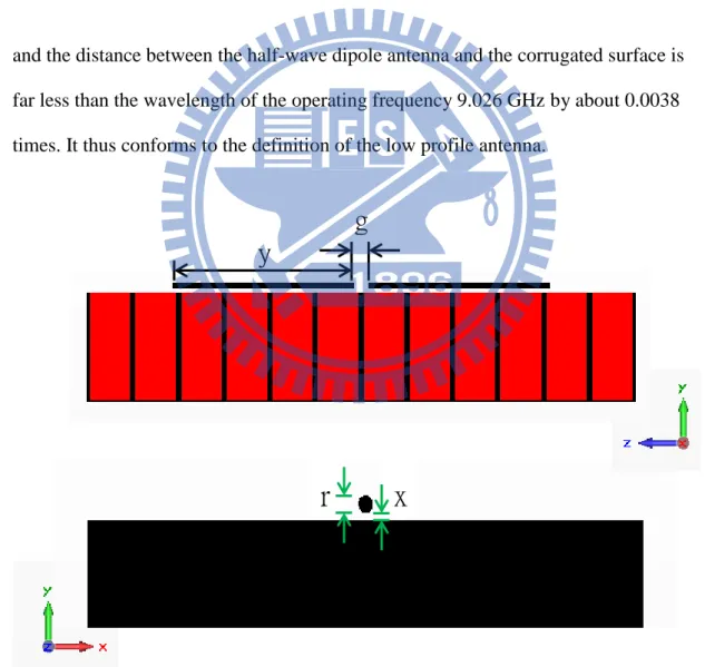
y = 6.81 mm, g = 0.544 mm, r = 0.25 mm, x = 0.125 mm,
and the distance between the half-wave dipole antenna and the corrugated surface is far less than the wavelength of the operating frequency 9.026 GHz by about 0.0038 times. It thus conforms to the definition of the low profile antenna.
r
x
g
y
Figure 2.4 The dimension of the low profile antenna composed of the half-wave dipole antenna and the corrugated surface.
15
Step 2: utilize the simulation software to substitute the PMC for the corrugated surface as shown in Figure 2.5.
Step 3: find out the position of the input impedance in the Smith chart of the low profile antenna which is substituted by the PMC in Figure 2.5. Then we obtain its input impedance of about 180 ohms as shown in Figure 2.6.
Figure 2.5 Substitute the PMC for the corrugated surface.
Figure 2.6 The impedance of the low profile antenna composed of the PMC.
16
Step 4: matching circuit can be completed by many different ways, and here we will use the RO4003 printed circuit board as shown in Figure 2.7. Its parameters are
t = 0.178 mm, h= 0.508 mm, 𝜀𝑟 = 3.55,
and it will be designed as the transmission line network to complete this mission.
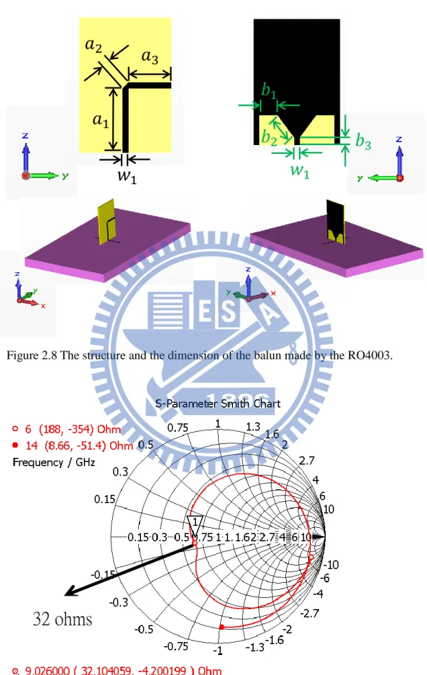
At first to equalize the current transiting into the half-wave dipole antenna, we need a balun structure as shown in Figure 2.8, and its parameters are
𝑎1 = 8.68 mm, 𝑎2 = 1.131 mm, 𝑎3 = 5.787 mm, 𝑤1 = 0.8 mm, 𝑏1 = 2.579 mm,
𝑏2 = 4.051 mm, 𝑏3 = 1.082 mm,
and there are two functions of this balun. One is to balance the current, and the other is to adjust the high input impedance to lower the input impedance by about 32 ohms as shown in Figure 2.9.
h
t
Figure 2.7 The dimension of the RO4003 printed circuit board.
Copper
17
Figure 2.8 The structure and the dimension of the balun made by the RO4003.
𝑎
1𝑎
2𝑎
3𝑏
1𝑏
2𝑏
3𝑤
1𝑤
1Figure 2.9 The impedance of the low profile antenna with the balun.
18
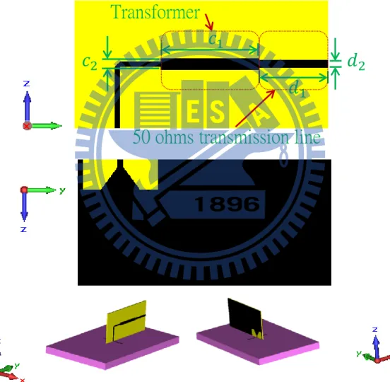
Then the quarter-wave transformer is utilized to cascade the balun and the 50 ohms transmission line as shown in Figure 2.10, and its parameters are
𝑐1 = 14.1 mm, 𝑐2 = 1.7 mm, 𝑑1 = 10 mm, 𝑑2 = 1.12 mm,
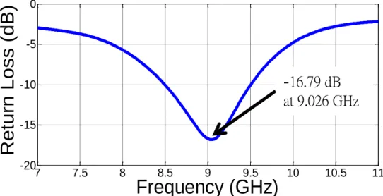
to complete the feeding network, and we will know the power can be transited in to it at 9.026 GHz because the return loss is about -16.79 dB as shown in Figure 2.11.
𝑐
2𝑐
1𝑑
1𝑑
2Figure 2.10 The structure and the dimension of the transformer to the 50 ohms transmission line.
Transformer
19
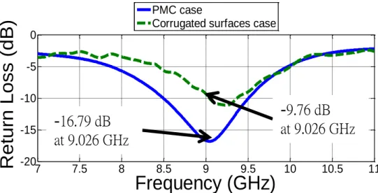
Step 5: change back the corrugated surface as shown in Figure 2.12, and then simulate its return loss as shown in Figure 2.13. Unfortunately, the result of the corrugated surface case does not have the same agreement with the PMC case, because the return loss of the corrugated surface case is only about -9.76 dB. We will explain why the result is not good and how to improve this in the next chapter.
7 7.5 8 8.5 9 9.5 10 10.5 11 -20 -15 -10 -5 0
Frequency (GHz)
Retu
rn Lo
ss (dB
)
Figure 2.11 The return loss of the low profile antenna including the feeding network with the PMC.
-
16.79 dB
at 9.026 GHz
20
2.3 Verify the simulation result and the measurement
result
Although the example in Section 2.2 does not show good results, we still have to fabricate the actual structure and verify whether the simulations and the measurement results are the same or not. Then we fabricate the real corrugated surface which is similar to the simulation case as shown in Figure 2.14 (a), and measure its reflection phase to compare with the simulation result as shown in Figure 2.14 (b). In Figure 2.14 we can know the real corrugated surface is very similar to the simulation structure. 7 7.5 8 8.5 9 9.5 10 10.5 11 -20 -15 -10 -5 0
Frequency (GHz)
Retu
rn Lo
ss (dB
)
PMC caseCorrugated surfaces caseFigure 2.13 The return loss of the low profile antenna including the feeding network with the corrugated surface.
-
9.76 dB
at 9.026 GHz
-
16.79 dB
21
Then we proceed to fabricating the half-wave dipole antenna and the feeding circuit as shown in Figure 2.15 (a), and combine them as shown in Figure 2.15 (b). Now measure the return loss of the low profile antenna as shown in Figure 2.16, and we can find out at the frequency 9.026 GHz we concern the return loss is about -8.85 dB, and it is quite close to the simulation result.
(a)
(b)
Figure 2.14 (a)The fabrication of the corrugated surface. (b) Its reflection phase.
6 7 8 9 10 11 12 -200 -100 0 100 200 Frequency (GHz) R e fle ctio n P h a se ( d e g re e ) Simulation Measurement
22
Figure 2.15 (a)The fabrication of the feeding network. (b) The measurement situation of the low profile antenna.
(a) (b) 8 8.5 9 9.5 10 10.5 11 -18 -16 -14 -12 -10 -8 -6 -4 -2 0 Frequency (GHz) Return Lo ss (dB) Simulation Measurement
Figure 2.16 The return loss of the low profile antenna.
-9.76 dB
at 9.026 GHz
-8.85 dB
at 9.026 GHz
23
Chapter 3 Extract the AMC region of the HIS
from the radiation pattern of the traditional
antenna and the reflection phases of the HIS
At the example in Section 2.2, we obtained a result that we do not expect. Therefore finding out which step is wrong becomes the most important mission. After checking the five steps, it is obvious that step 1 is already wrong in that example because step 2 to step 5 are based on the hypothesis of the correct AMC region at step 1, and only if step 1 is correct, the other steps can become functional. In this chapter we aim to find out the AMC region of the HIS when designing the low profile antenna, and also adjust the example in Section 2.2 to achieve a complete design of the low profile antenna.
3.1 The radiation pattern of the traditional half-wave
dipole antenna
From step 1 in Section 2.2 the AMC region of the HIS can be determined by using the reflection phase according to the general definition. However, this does not consider the radiation pattern of the antenna. Because the reflection phase of the general definition is defined by the normal incident wave, the waves excited by the traditional antenna on the HIS are not all normal incident waves toward the HIS. Therefore surveying the pattern of the traditional antenna becomes the priority. To adjust the example in Section 2.2, we should understand the radiation pattern of the half-wave dipole antenna as shown in Figure 3.1.
24
From Figure 3.1 we can know the electromagnetic waves radiated by the half-wave dipole antenna are the strongest towards every direction in the yz plane. Therefore when this antenna is put on the HIS, it is very important to consider that there are many electromagnetic waves with different directions which affect the HIS as shown in Figure 3.2. This is why the example in Section 2.2 has the wrong result because of considering the reflection phase determined only by the normal incident wave.
Figure 3.1 (a) The 3D pattern of the half-wave dipole antenna. (b) The yz plane pattern.
(b) (a)
HIS
Figure 3.2 The waves exited by the half-wave dipole antenna illuminate the HIS with different angles and strengths.
25
3.2 The global definition of the reflection phase
Global definition: consider an infinite periodic structure illuminated by a plane wave arriving from an arbitrary incident angle [6, 11]. The phase difference of the electric field between the incident wave and the reflected wave is the global reflection phase of the structure. Moreover, the global reflection phases whose electric fields are parallel with the surface under test are 𝑇𝐸𝜃 modes and the global reflection phases whose magnetic fields are parallel with the surface under test are 𝑇𝑀𝜃 modes, as shown in Figure 3.3.
Measurement: the approach is the same as that of Section 1.4. Use two horn antennas to measure the surface under test, and the difference is that in Section 1.4 we transmit the normal incident wave and in this section we transmit incident waves with different angles when needing the different global reflection phases as shown in Figure 1.1 (a). The global reflection phase varies with θ as shown in Figure 3.4 (b).
Surface under test
Surface under test
𝑘
𝑖𝑛⃑⃑⃑⃑⃑
𝐸
𝑖𝑛⃑⃑⃑⃑⃑
𝐻
𝑖𝑛⃑⃑⃑⃑⃑⃑
θ
𝑘
⃑⃑⃑⃑⃑
𝑖𝑛𝐸
𝑖𝑛⃑⃑⃑⃑⃑
θ
𝐻
𝑖𝑛⃑⃑⃑⃑⃑⃑
(a) (b)Figure 3.3 (a) The 𝑇𝐸𝜃 definition of the reflection phase. (b) The 𝑇𝑀𝜃 definition of the reflection phase.
𝐸
𝑜𝑢𝑡⃑⃑⃑⃑⃑⃑⃑⃑
𝑘
𝑜𝑢𝑡⃑⃑⃑⃑⃑⃑⃑⃑
𝐻
𝑜𝑢𝑡⃑⃑⃑⃑⃑⃑⃑⃑⃑
𝐻
𝑜𝑢𝑡⃑⃑⃑⃑⃑⃑⃑⃑⃑
𝑘
𝑜𝑢𝑡⃑⃑⃑⃑⃑⃑⃑⃑
𝐸
𝑜𝑢𝑡⃑⃑⃑⃑⃑⃑⃑⃑
26
3.3 Extract the AMC region of the HIS
In Section 3.1 we already know that the greatest strengths of the pattern radiate toward the corrugated surface in the yz plane, and in the yz plane the electric fields of the incident waves are parallel with the corrugated surface, so they are all 𝑇𝐸𝜃
modes as shown in Figure 3.5. Therefore we need to obtain the 𝑇𝐸𝜃 mode data of the
(a)
Surface
under test
Transmitting
horn antenna
Receiving
horn antenna
Absorber
θ
𝑇𝐸
𝜃 (b)Figure 3.4 (a) The measurement method of the global reflection phase. (b) Three examples of the 𝑇𝐸𝜃 mode.
0 2 4 6 8 10 12 14 16 18 -200 -150 -100 -50 0 50 100 150 200 Frequency (GHz) Reflection Phase (de gree) θ = 0° θ = 40° θ = 70°
27
global reflection phases between θ = −90° and θ = 90° to extract the correct AMC region of the corrugated surface in Section 2.2.
The four 𝑇𝐸𝜃 mode samples of the corrugated surface in Section 2.2 are as shown in Figure 3.6 which are computed by CST software. We need to find a way to obtain the key point of step 1 in the standard flow chart of feeding low profile antenna: and confirm the hypothesis of the AMC region.
Corrugated surface
𝑘⃑
𝐸⃑
𝑘⃑
𝑘⃑
𝐸⃑
𝐸⃑
Figure 3.5 The 𝑇𝐸𝜃 mode waves excited by the half-wave dipole antenna on the corrugated surface.
y
z
𝑇𝐸
𝜃 0 2 4 6 8 10 12 14 16 18 -200 -150 -100 -50 0 50 100 150 200Frequency (GHz)
Reflection
Phase
(degree)
θ = 0° θ = 30° θ = 60° θ = 80°28
From Figure 3.6 we can observe that 𝑇𝐸0° curve is what we use to judge the AMC region of the corrugated surface, because the global reflection phase 𝑇𝐸𝜃 mode which θ = 0° is the same as the general definition of the reflection phase. It is obvious that only considering the 𝑻𝑬𝟎° is not enough. According to the radiation
pattern in Section 3.1, we can observe that the most interactions with the corrugated surface are all the 𝑇𝐸𝜃 modes, so the AMC region of the corrugated surface must be deeply related with the 𝑇𝐸𝜃 mode waves. Moreover, their radiation strengths are the same, so there is a method to find out the AMC region of the corrugated surface: average these global reflection phase 𝑇𝐸𝜃 modes which represent the most
interactions between the half-wave dipole antenna and the corrugated surface, and these global reflection phase 𝑇𝐸𝜃 modes we need are over the range between θ = −90° and θ = 90° as shown in Equation 1.
𝑅𝑒(𝑓) = ∫−90°90° 𝑇𝐸𝜃(𝑓)𝑑𝜃 (1)
The 𝑅𝑒 represents the effective reflection phase that we use to define the AMC region of the HIS when we use the standard flow chart of feeding the low profile antenna to design the matching circuit. The frequency of the 0° effective reflection phase is where the HIS is most similar to the PMC in the case of the low profile antenna composed of the traditional antenna and the HIS. Comparing with step 1 in Section 2.2, that way seems very rough. Now we calculate the effective reflection phase by Equation 1, and then we obtain Figure 3.7. This is the really correct and effective way to use at the example in Section 2.2. In the following section we will utilize it well to design the feeding network of the low profile antenna.
29
3.4 Redesign the low profile antenna in Section 2.2 by
the effective reflection phase
From Section 3.1 to Section 3.3, we already know how to extract the AMC region of the HIS to design the low profile antenna. We have this key point, so we can make the standard flow chart of feeding the low profile antenna functional and working well. Now we adjust the example in Section 2.2, and show its effect.
Step 1: find out the effective AMC region of the corrugated surface as shown in Figure 3.8. After judging by the effective reflection phase, we can obtain the frequency as 9.945 GHz when the 𝑅𝑒 = 0°, and this is the frequency that the corrugated surface is most similar to the PMC.
0 2 4 6 8 10 12 14 16 18 -200 -150 -100 -50 0 50 100 150 200 Frequency (GHz) Reflection Phase (de gree)
30
At this example we can combine the low profile antenna with the half-wave dipole antenna operating near 9.945 GHz and the corrugated surface as shown in Figure 2.4, and its parameters are
y = 6.155 mm, g = 0.544 mm, r = 0.25 mm, x = 0.125 mm,
and the distance between the half-wave dipole antenna and the corrugated surface is far less than the wavelength of the operating frequency 9.945 GHz by about 0.0041 times. It thus conforms to the definition of the low profile antenna.
Step 2: utilize the simulation software to substitute the PMC for the corrugated surface as shown in Figure 2.5.
Step 3: find out the position of the input impedance in the Smith chart of the low
0 2 4 6 8 10 12 14 16 18 -200 -150 -100 -50 0 50 100 150 200 Frequency (GHz) Reflection Phase (de gree)
Figure 3.8 The corrugated surface’s effective reflection phase is 0° at 9.945 GHz.
31
profile antenna which is substituted by the PMC in Figure 2.5. Then we obtain its input impedance is about 180 ohms as shown in Figure 3.9.
Step 4: use the printed circuit board RO4003 to achieve this mission. Design a balun structure as shown in Figure 3.10, and its parameters are
𝑎1 = 7.899 mm, 𝑎2 = 1.131 mm, 𝑎3 = 5.266 mm, 𝑤1 = 0.8 mm, 𝑏1 = 2.311 mm, 𝑏2 = 3.597 mm, 𝑏3 = 1.069 mm,
and this balun has two functions. One is to balance the current and the other one is to adjust the higher impedance in the Smith chart to the lower impedance of about 31 ohms, as shown in Figure 3.11.
Figure 3.9 The impedance of the low profile antenna composed of the PMC.
32
Figure 3.10 The structure and the dimension of the balun made by the RO4003.
𝑎
1𝑎
2𝑎
3𝑏
1𝑏
2𝑏
3𝑤
1𝑤
1Figure 3.11 The impedance of the low profile antenna with the balun.
33
Then utilize the quarter-wave transformer to cascade the balun and the 50 ohms transmission line as shown in Figure 3.12, and its parameters are
𝑐1 = 12.75 mm, 𝑐2 = 1.72 mm, 𝑑1 = 10 mm, 𝑑2 = 1.12 mm,
to complete the feeding network, and we will know the power can be transited in to it at 9.945 GHz because the return loss is about -16.38 dB as shown in Figure 3.13.
𝑐
2𝑐
1𝑑
1𝑑
2Figure 3.12 The structure and the dimension of the transformer to the 50 ohms transmission line.
Transformer
34
Step 5: change the corrugated surface back again as shown in Figure 3.14. Then simulate its return loss as shown in Figure 3.15, and we can obtain the return loss is about -17.85 dB at 9.945 GHz. This simulation result is exciting because it confirms
that the AMC region of the HIS we find out is correct, and proves the standard
flow chart of feeding the low profile antenna is very functional.
7 7.5 8 8.5 9 9.5 10 10.5 11 -20 -15 -10 -5
Frequency (GHz)
Retu
rn Lo
ss (dB
)
Figure 3.13 The return loss of the low profile antenna including the feeding network with the PMC.
-16.38 dB
at 9.945 GHz
35
3.5 Verify the simulation result and the measurement
result
Although the results in Section 3.4 conform to our expectation, we still have to verify whether the simulation and the fabrication are the same or not. As such, we measure the global reflection phases of a manufactured prototype and compare with the
simulation results, as shown in Figure 3.16. We can observe that the measured and the simulated reflection phases are in decently approximate agreement.
7 7.5 8 8.5 9 9.5 10 10.5 11 -20 -15 -10 -5 0
Frequency (GHz)
Retu
rn Lo
ss (dB
)
PMC caseCorrugated surfaces caseFigure 3.15 The return loss of the low profile antenna including the feeding network with the corrugated surface.
-
16.38 dB
at 9.945 GHz
-
17.85 dB
36
We manufacture the feeding circuit as shown in Figure 3.17 (a), and the whole low profile antenna is accomplished as shown in Figure 3.17 (b). After measuring this low
Figure 3.16 The fabrication of the corrugated surface’s global reflection phase examples. 6 7 8 9 10 11 12 -200 -100 0 100 200 Frequency (GHz) R e fle ctio n P h a se ( d e g re e ) TE 0° Simulation Measurement 6 7 8 9 10 11 12 -200 -100 0 100 200 Frequency (GHz) Ref le ctio n P h a se ( d e g re e ) TE 40° Simulation Measurement 6 7 8 9 10 11 12 -150 -100 -50 0 50 100 150 200 Ref le ctio n P h a se ( d e g re e ) TE 60° Frequency (GHz) Simulation Measurement
37
profile antenna, we get the return loss as shown in Figure 3.18, and it is about -17.95 dB at 9.945 GHz. It shows good agreement with the simulation result.
Figure 3.17 (a)The fabrication of the feeding network. (b) The measurement situation of the low profile antenna.
(a) (b) 8 8.5 9 9.5 10 10.5 11 -20 -18 -16 -14 -12 -10 -8 -6 -4 -2 0 Frequency (GHz) R e tu rn L o ss ( d B ) Simulation Measurement
Figure 3.18 The return loss of the low profile antenna.
-17.85 dB
at 9.945 GHz
-17.95 dB
at 9.945 GHz
38
Chapter 4 Apply to the different type of the HIS
In the previous three chapters we have described the standard procedure of how to design the low profile antenna, and also have used two examples to show how to utilize the procedure. In this chapter we will aim to extend to another HIS structure, to verify the repeatability of the procedure.
4.1 Frequency selective surface (FSS)
In the previous two chapters, the two examples all used the corrugated surface to represent the HIS, and utilized our extraction method from those global reflection phases to approach the PMC property. In this chapter, we will adapt the FSS [12] to design the low profile antenna, and the emphasis of this chapter is that, if we can utilize the same systematic procedure to complete the design of different types of the HIS, then this systematic procedure will be effective and powerful. The dimension and the structure of the FSS we use are as shown in Figure 4.1.Its parameters are
w = 6 mm, g = 1 mm, t = 0.035 mm, h = 1.6 mm, 𝜀𝑟 = 4.3,
39
4.2 Calculate the effective reflection phase according
to the radiation pattern of the traditional antenna
To compare the difference, we still use the half-wave dipole antenna as our traditional antenna, and the only difference is that the FSS is substituted for the corrugated
surface. The same method as in Section 3.3 is then carried out. As shown in Figure 3.5, the global reflection phase 𝑇𝐸𝜃 modes of the FSS between θ = −90° and θ = 90° which are computed by CST software is first obtained as shown in Figure 4.2 (a), Equation 1 is then used to calculate the effective reflection phase from which the low profile antenna can be designed, as shown in Figure 4.2 (b).
Figure 4.1 The structure and the dimension of the FSS.
Side view
Top view
Dielectric (𝜀
𝑟)
w
w
g
g
t
t
h
40
(a)
Figure 4.2 (a) The reflection phases of the FSS. (b) The FSS’ effective reflection phase is 0° at 8.44 GHz. 0 2 4 6 8 10 12 14 -200 -150 -100 -50 0 50 100 150 200 Frequency (GHz) Reflection Phase (de gree) 0 2 4 6 8 10 12 14 -200 -150 -100 -50 0 50 100 150 200 Frequency (GHz) Reflection Phase (de gree) θ = 0° θ = 40° θ = 60° θ = 80°
𝑇𝐸
𝜃 (b)0° at 8.44 GHz
41
4.3 Utilize the standard flow chart to design the low
profile antenna
Step 1: by the calculation procedure for the effective reflection phase as laid out in in Section 4.2, the frequency corresponding to zero phase is 8.44 GHz. Therefore we combine the low profile antenna with the half-wave dipole antenna operating near 8.44 GHz and the FSS in Section 4.1 as shown in Figure 4.3, and its parameters are
y = 7.381 mm, g = 0.544 mm, r = 0.5 mm, x = 0.09 mm,
and the distance between the half-wave dipole antenna and the FSS is far less than the wavelength of the operating frequency about 0.0025 times. It conforms to the
definition of the low profile antenna.
Figure 4.3 The dimension of the low profile antenna composed of the half-wave dipole antenna and the FSS.
y
r
x
42
Step 2: utilize the software to substitute the PMC for the FSS, as shown in Figure 4.4.
Step 3: from the Smith chart, find out the position of the input impedance of the low profile antenna which is substituted by the PMC in Figure 4.4. Its input impedance is found to be about 193 ohms as shown in Figure 4.5.
43
Step 4: use the printed circuit board RO4003 to achieve this mission. Design a balun structure as shown in Figure 4.6, and its parameters are
𝑎1 = 5 mm, 𝑎2 = 1.131 mm, 𝑎3 = 11 mm, 𝑤1 = 0.8 mm, 𝑏1 = 3.623 mm, 𝑏2 = 1.381 mm, 𝑏3 = 2.773 mm,
and there are two functions of this balun. One is to balance the current, and the other one is to adjust the high input impedance to lower the input impedance to about 22 ohms as shown in Figure 4.7.
193 ohms
44
Figure 4.6 The structure and the dimension of the balun made by the RO4003.
𝑎
1𝑎
2𝑎
3𝑏
2𝑏
3𝑤
1𝑤
1𝑏
1𝑏
145
Then utilize the quarter-wave transformer to cascade the balun and the 50 ohms transmission line as shown in Figure 4.8, and its parameters are
𝑐1 = 5.2 mm, 𝑐2 = 2.01 mm, 𝑑1 = 5 mm, 𝑑2 = 1.12 mm,
to complete the feeding network, and we will know the power can be transited in to it at 8.44 GHz because the return loss is about -26.81 dB as shown in Figure 4.9.
Figure 4.7 The impedance of the low profile antenna with the balun.
46
𝑐
2𝑐
1𝑑
1𝑑
2Figure 4.8 The structure and the dimension of the transformer to the 50 ohms transmission line.
Transformer
50 ohms transmission line
7 7.5 8 8.5 9 9.5 10 10.5 11 -35 -30 -25 -20 -15 -10 -5 0 Return Lo ss (dB) Frequency (GHz)
Figure 4.9 The return loss of the low profile antenna including the feeding network with the PMC.
-26.81 dB
at 8.44 GHz
47
Step 5: change the FSS back again as shown in Figure 4.10. Then simulate its return loss as shown in Figure 4.11, and the return loss is about -26.74 dB at 8.44 GHz. This simulation result conforms well to our expectation. This ensures that this newly formulated method is a systematic and repeatable one that is applicable to different types of HIS.
48
4.4 Verify the simulation result and the measurement
result
Although the results in Section 4.4 conform to our expectation, we still have to verify whether the simulations and the measurement performed on a manufactured prototype are the same or not. The real fabricated FSS is photographed in Figure 4.12 (a) and measure its global reflection phases and compare with the simulation results, as shown in Figure 4.12 (b). We can observe that the fabrication and the simulation are very approximate. 7 7.5 8 8.5 9 9.5 10 10.5 11 -35 -30 -25 -20 -15 -10 -5 0 Frequency (GHz) Return Lo ss (dB) PMC case FSS case
Figure 4.11 The return loss of the low profile antenna including the feeding network with the FSS.
-
26.81 dB
at 8.44 GHz
-
26.74 dB
at 8.44 GHz
49
(a)
(b)
Figure 4.12 (a)The fabrication of the FSS. (b) Its reflection phases.
6 7 8 9 10 11 12 -200 -100 0 100 200 Frequency (GHz) R e fle ctio n P h a se ( d e g re e ) TE 0° Simulation Measurement 6 7 8 9 10 11 12 -200 -100 0 100 200 Frequency (GHz) R e fle ctio n P h a se ( d e g re e ) TE 40° Simulation Measurement 6 7 8 9 10 11 12 -200 -100 0 100 200 Frequency (GHz) R e fle ctio n P h a se ( d e g re e ) TE 60° Simulation Measurement
50
We manufacture the feeding circuit as shown in Figure 4.13 (a), and the whole low profile antenna is accomplished as shown in Figure 4.13 (b). After measuring this low profile antenna, we get the return loss as shown in Figure 4.14, and it is about -26.14 dB at 8.44 GHz. It shows good agreement with the simulation result.
Figure 4.13 (a)The fabrication of the feeding network. (b) The measurement situation of the low profile antenna.
(a) (b) 7 7.5 8 8.5 9 9.5 10 10.5 11 -35 -30 -25 -20 -15 -10 -5 0 Frequency (GHz) Return Lo ss (dB) Simulation Measurement
Figure 4.14 The return loss of the low profile antenna.
-26.74 dB
at 8.44 GHz
-26.14 dB
at 8.44 GHz
51
Chapter 5 Apply to the different type of the
traditional antenna
In Chapter 4 we succeeded in demonstrating that the design procedure of the proposed standard flow chart can be applied to different types of HIS. In this chapter we will take on the challenge of using different types of traditional antenna. Now we still maintain the research principle of changing one condition at a time when comparing the experiments. In this chapter we will confirm again that when designing the low profile antenna, how to determine the AMC region of the HIS is deeply related to the radiation pattern of the traditional antenna at step 1 of the standard flow chart. In the following section we will adapt the folded dipole antenna and the FSS structure in Chapter 4 to combine a low profile antenna.
5.1 The structure and the radiation pattern of the
traditional folded dipole antenna
The structure of the folded dipole antenna as shown in Figure 5.1, and this antenna is applied widely in our life. Generally its total length is almost the half wavelength of the operating frequency. Its 3D pattern is as shown in Figure 5.2 (a) and it has the most radiation pattern and the similar strengths every direction in the yz plane as shown in Figure 5.2 (b).
Figure 5.1 The shape of the folded dipole antenna.
52
5.2 Extract the AMC region of the FSS
In Section 5.1 we already know the pattern of the folded dipole antenna has the approximate strengths in the yz plane, and the electric fields of the waves excited by the folded dipole antenna are all parallel with the FSS as shown in Figure 5.3. Therefore we should obtain the data of the global reflection phase 𝑇𝐸𝜃 modes whose θ between −90° and 90° have been as shown in Figure 4.2 (a). We have also extracted the effective reflection phase from those global reflection phase 𝑇𝐸𝜃 modes for this folded dipole antenna as shown in Figure 4.2 (b).
Figure 5.2 (a) The 3D pattern of the folded half-wave dipole antenna. (b) The yz plane pattern.
(b) (a)
53
5.3 Utilize the standard flow to design the low profile
antenna
Step 1: in Section 5.2 we got the effective reflection phase, and the frequency corresponding to zero phase is 8.44 GHz. Therefore we adapt the folded dipole antenna operating near 8.44 GHz and the FSS structure in Section 4.1 to combine the low profile antenna as shown in Figure 5.4. Its parameters are
w = 1.1 mm, q = 0.1 mm, y = 7.384 mm, g = 0.544 mm, r = 0.5 mm, x = 0.09 mm,
and the distance between the folded dipole antenna and the FSS is far less than the wavelength of the operating frequency 8.44 GHz about 0.0025 times, so it conforms to the definition of the low profile antenna.
FSS
𝑘⃑
𝐸⃑
𝑘⃑
𝑘⃑
𝐸⃑
𝐸⃑
54
Step 2: utilize the software to substitute the PMC for the FSS, as shown in Figure 5.5.
Step 3: from the Smith chart, find out the position of the input impedance of the low profile antenna which is substituted by the PMC in Figure 5.5. Its input impedance is
Figure 5.4 The dimension of the low profile antenna composed of the folded half-wave dipole antenna and the FSS.
r
x
y
g
w
q
55
found to be about 511 + 336i ohms as shown in Figure 5.6.
Step 4: use the printed circuit board RO4003 to achieve this mission. Design a balun structure as shown in Figure 5.7, and its parameters are
𝑎1 = 6.345 mm, 𝑎2 = 10.925 mm, 𝑤1 = 0.5 mm, 𝑏1 = 2.008 mm, 𝑏2 = 1.896 mm,
𝑏3 = 1.5 mm,
and there are two functions of this balun. One is to balance the current, and the other one is to adjust the high input impedance to lower the input impedance to about 10 ohms as shown in Figure 5.8.
Figure 5.6 The impedance of the low profile antenna composed of the PMC.
56
Figure 5.7 The structure and the dimension of the balun made by the RO4003.
𝑎
1𝑎
2𝑏
1𝑏
2𝑏
3𝑤
1𝑤
157
Then utilize the quarter-wave transformer to cascade the balun and the 50 ohms transmission line as shown in Figure 5.9, and its parameters are
𝑐1 = 4.66 mm, 𝑐2 = 3.351 mm, 𝑑1 = 5 mm, 𝑑2 = 1.12 mm,
to complete the feeding network, and we will know the power can be transited in to it at 8.44 GHz because the return loss is about -20.15 dB as shown in Figure 5.10.
Figure 5.8 The impedance of the low profile antenna with the balun.
58
𝑐
2𝑐
1𝑑
1𝑑
2Figure 5.9 The structure and the dimension of the transformer to the 50 ohms transmission line.
Transformer
50 ohms transmission line
7 7.5 8 8.5 9 9.5 10 10.5 11 -25 -20 -15 -10 -5 0 Frequency (GHz) Return Lo ss (dB)
Figure 5.10 The return loss of the low profile antenna including the feeding network with the PMC.
-20.15 dB
at 8.44 GHz
59
Step 5: change the FSS back again as shown in Figure 5.11. Then simulate its return loss as shown in Figure 5.12, and the return loss is about -20.57 dB at 8.44 GHz. This simulation result conforms well to our expectation. Consequently, we prove again that considering the radiation pattern of the different type of the traditional antenna is necessary.
Figure 5.11 Substitute the FSS for the PMC back.
7 7.5 8 8.5 9 9.5 10 10.5 11 -25 -20 -15 -10 -5 0 Frequency (GHz) Return Lo ss(dB) PMC case FSS case
Figure 5.12 The return loss of the low profile antenna including the feeding network with the FSS.
-
20.57 dB
at 8.44 GHz
-
20.15 dB
60
5.4 Verify the simulation result and the measurement
result
Although the results in Section 5.3 conform to our expectation, we still have to verify whether the simulations and the measurements performed on a manufactured
prototype are the same or not. The real fabricated FSS and its global reflection phases have been as shown in Figure 4.12.
We manufacture the feeding circuit as shown in Figure 5.13 (a), and the whole low profile antenna is accomplished as shown in Figure 5.13 (b). After measuring this low profile antenna, we get the return loss as shown in Figure 5.14, and it is about -20.44 dB at 8.44 GHz. It shows good agreement with the simulation result.
61
Figure 5.13 (a)The fabrication of the feeding network. (b) The measurement situation of the low profile antenna.
(a) (b) 7 7.5 8 8.5 9 9.5 10 10.5 11 -25 -20 -15 -10 -5 0 5 Frequency (GHz) Return Lo ss (dB) Simulation Measurement
Figure 5.14 The return loss of the low profile antenna.
-20.57 dB
at 8.44 GHz
-20.44 dB
at 8.44 GHz
62
Chapter 6 Conclusion
After surveying many researches about the low profile antenna design, we can observe that there are a lot of ways to transmit the power to the low profile antenna. However, the methods of feeding the low profile antenna are case by case, it will cost the researchers a lot of time to try and tune their structure to reach the purpose of getting the good return loss. In view of this, developing the standard design flow seems a milestone of the upgrade about the low profile antenna design. In Chapter 2 we create the procedure but still lack a key of finding out the AMC region.
Consequently in Chapter 3 we grasp the key to solve that issue, and get a very good result. But we think it is still not enough, we should experiment with more cases of different kind of the HIS and the traditional antenna to confirm the truth of the good function of this standard design flow chart. Therefore we extend this procedure to the different kind of the HIS in Chapter 4 and the different kind of the traditional antenna in Chapter 5, and the results are also show the very good agreement with our
expectation. We hope this systematic method can provide those researchers study in the low profile antenna the simple and clear way to transmit the power to their low profile antenna.