Crossover Phenomenon in Oxidation Rates of the
(110) and (111) Orientations of Silicon in N20
T. S. Chao*
National Nano Device Laboratory, Hsinchu 300, Taiwan
T. F, Lei
Institute of Electronic, National Chiao Tung University, Hsinchu 300, Taiwan
ABSTRACT
Growth mechanisms of three different orientations Si wafer oxidized in NzO have been investigated in this study. A thickness crossover phenomenon in oxidation rates was found for orientations (110) and (111) at a critical oxide thickness 150 A. From our results, this phenomenon is closely related with the initial native oxide before oxidation.
Introduction
Recently, N20
oxide has been widely studied as the gate oxide for future submicron devices. This is because oxides grown in N20 ambient, instead of the conventional 02 ambient, 1'2 exhibit an im- proved performance, such as lower interfacial densities, stronger immunities of hot electrons, etc. The reason for these improve- ments results from a piling up of a nitrogen layer forming at the interface of SiOz/Si. 3-4 As for the trend of the technology, gate oxide of thickness 80-90 A is required for the 0.35 t~m technology, and 60-70 ~, for 0.25 t~m, respectively. However, it is impossible to avoid a native oxide, - 2 0 A, growing on the silicon surface during the sample preparation and before high temperature oxidation. The thickness of this native oxide is almost one-third to one-fourth of the final thickness. Therefore, the native oxide is of most concern when an ultrathin gate oxide is required with good uniformity and quality. Silicon oxidized in 02 ambient is the conventional method to grow oxide on Si substrates. The growth rate of oxide depends on tem- perature, crystal orientation, pressure, ambient impurities, and sili- con doping. For the orientation effect, it has been reported by irene et aL s that the rate of oxidation, R, has the initial order R(110) > R(111) > R(100). However, at thicker regimes, the order changes to R(111) > R(110) > R(100). They consider that this crossover phenomenon of (111) and (110) is attributed to the effect of me- chanical stress at the interface on the surface reaction.In this study, Si wafers oxidized in NzO ambient are investigated. The crossover phenomenon observed in O2 oxidation is found also in the N20 ambient. Different thicknesses of native oxide grown on the different orientations of the Si surface before oxidation are proposed as an explanation of this phenomenon.
* Electrochemical Society Active Member.
400 350 300 250 200
15oi
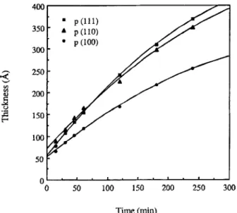
100 50 o 0 9 ! i I 9 i . i . | . 50 100 150 200 250 300 T i m e (min)Fig. 1. The thickness of oxide grown in N20 ambient v s . time at 1000~ Three orientations (111), (110), and (100) of wafers were investigated.
L34
Experimental and Results
p-Type 4 in. wafers with resistivity 15-25 Q,-cm were used. Wafers were cleaned with the RCA cleaning process and dipped into HF:H20 = 1:50 to remove native oxide. Before oxidation, ellip- sometry measurements were performed on the different samples. The ellipsometric angles, ~. and ~, are close to the ideal value of bare silicon, 179.25 ~ and 10.39 ~ respectively. Substrate roughness was measured by atomic force microscopy (AFM). All samples had a root-mean-square (rms) roughness under 1.3 A which means the substrate roughness is atomically flat. Oxidation was performed in a conventional resistance-heated diffusion furnace with computer control of flows and temperature. The concentration of N20 gas was 99.9995% with moisture less than 0.5 ppm. The growth pres- sure was 1 atm. Oxide thicknesses were measured by ellipsometry with a fixed index of refraction of 1.465. 6 The orientations of wafers, (111), (110), and (100) were used. The growth temperature was 1000~ Wafers were loaded into the furnace at 700~ in N2 ambi- ent, and ramped up to 1000~ in 45 rain and stabilized at 1000~ for 10 min. Then N20 gas was introduced. The growth time was in a range of 0.5 to 4 h. The thickness at 9 points over the whole wafer was measured. The thickness of oxide growth with time is shown in Fig. 1. The uniformity was +2 A. The growth rate for (100) was the lowest one which was the same as in the 02 ambient. For the first hour of oxidation, the thickness of (110) was larger than that of (111). However, the (111) orientation had a steep slope, Le., higher growth rate, than (110). From Fig. 1, we can see that after 75 min, on the contrary, the thickness of-(111 ) was larger than (110): There was a crossover point - 7 5 min with thickness about 172 A. After this point, the growth entered into the parabolic regime. The growth mechanism in the initial linear regime can be modeled simply by the equation 7
To• = Rt + To [1]
Where R is the linear growth rate; To is the oxide thickness at growth time t = 0, and Tox is the oxide thickness. The R can be extrapolated from Fig. 1. The linear growth rate for (111 ), (110), and (100) were 1.72, 1.68, and 1.15 A/min, respectively. However, the To cannot be found easily as time was zero. To make this growth mechanism clear, another experiment was performed. Wafers of (111), (110), and (100) were put into the furnace under the same thermal cycles of the former oxidation processes excepting the N20
Table I. The measured ellipsometric angles of 4, W, and thicknesses of native oxides on silicon substrates of
different orientations (110), (100), and (111).
~ S.D.~of & S.D. of 9 Thickness Orien~tion (deg~e) (deg~e) (degree) (deg~e) (A) <110> 169.82 10.58 0.00063 0.0037 32.3 <100> 170.82 10.54 0.00189 0.0029 29.2 <111> 170.97 10.54 0.00618 0.0003 28.6
aS.D. = standard deviation.
J. Electrochem. Soc., Vol. 142, No. 3, March 1995 9 The Electrochemical Society, Inc.
) unless CC License in place (see abstract).
ecsdl.org/site/terms_use
address. Redistribution subject to ECS terms of use (see
140.113.38.11
J. Electrochem. Soc., Vol. 142, No. 3, March 1995 9 The Electrochemical Society, Inc. L35
180
10.6178
176
I74
172
170
168
0
1 ~0
1 ~5
2~0
2~5
30
35
Thickness (,~)
G"
10.5 1o.4 b 10.3 05
1'0
2'0
2'5
3o
35
Thickness (A)
I 9 N=1.460 9 N=1.465 --N=1.470]
Fig. 2. (a, top) The simulated ~ v s . thickness of native oxide with refractive index of 1.460, 1.465, and 1.470. Incident angle is 70.0 ~ and wavelength is 632.8 nm. (b, bottom) The simulated
v s . thickness of native oxide with refractive index of 1.460,
1.465, and 1.470.
oxidation processes. The temperature ramped up from 700 to 1000~ stabilizing for 10 min at the temperature of 1000~ then ramped down to 700~ All the processes were in the pure N2 ambient. Thicknesses of the native oxides of the various orienta- tions were measured again by ellipsometer. Table I shows the measured ellipsometric angles. Nine points over the whole wafers were measured. The standard deviations of z~ and 9 were small. This implied the thickness was uniform. The thickness measured from 2x and 9 was calculated by using 8
Tox = f(&, q~, h, cb, na, nox, n,, ks) [2] where ~b is the incident angle of 70 ~ na (1.0) and nox (1.465) are the index of refraction of air and oxide, respectively, n~, and ks are the
real and imaginary parts of the index of the silicon substrate at wavelength X of 632.8 nm. The advantage of fixed nox to calculate the thickness is to reduce the instrument and system errors, espe- cially at the oxide thickness of oxide under 200 A. 6 Thickness for the orientation (110) was the largest one among these three orien- tations. The thicknesses of the native oxides were 28.6, 32.2, and 29.2 A for orientations (111), (110), and (100), respectively. The higher initial oxidation rate of (110) orientations was expected on the basis of the areal density of silicon atoms in different planes of (110), (111), and (100). To investigate the error from the deviation of refractive index on the calculated oxide thickness, Fig. 2a and b show the & and 9 vs. thickness with no• in the range of 1.460, 1.465, and 1.470. From these two figures, the differences among these three lines were small. As the thickness was less than 35 A, the thickness deviation was only I A if a 0.005 deviation is included in nox. Hence, the thickness calculated in Table I was believable and precise. According to Eq. 1, the growth thickness for (111) and (110) can be written as
Tox(111) = 1.72t + 28.6 [3]
"/-o• = 1.68t + 32.3 [4]
Where 1.72 A/min, 1.68 ~Jmin, 28.6 A, and 32.3 A, are the R(111 ), R(110), To(111 ), and To(110), respectively. The crossover point can be calculated from Eq. 3 and 4 at t = 74 min, and To• = 156 A. These two values were close to the estimated values of time t = 75 min, and Tox = 172 A in Fig. 1.
Conclusion
In this paper, a crossover phenomenon in oxidation rates of orientations (111) and (110) of silicon oxidized in N20 was re- ported. This phenomenon can be explained successfully by consid- ering the native oxide before oxidation. Orientation of (110) has the largest native oxide thickness among the three investigated orien- tations that results in a thicker thickness than (111) in the initial oxidation regime.
Acknowledgments
The authors thank Mr. H. Y. Chang and Dr. S. C. Sun for sample preparations, and the National Science Council of the Republic of China for financial support.
Manuscript submitted August 22, 1994; revised manuscript re- ceived Dec. 8, 1994.
National Nano Device Laboratory assisted in meeting the publi- cation costs of this article.
REFERENCES
1. W. Ting, G. Q. Lo, J. Ahn, T. Y. Chu, and D. L. Kwong, IEEE Electron Device Lett., EDL-12, 416 (1991 ).
2. 7. Liu, H. J. Wann, P. K. Ko, C. Hu, and Y. C. Cheng, ibid., EDL-13, 402 (1992).
3. Y. Okada, P. J. Tobin, V. Lakhotia, W. A. Fell, S. A. Ajuria, and R. I. Hegde, AppL Phys. Lett., 63, 194 (1993).
4. T. S. Chao, W. H. Chen, S. C. Sun, and H. Y. Chang, This Journal, 140, 2905 (1993).
5. E. A. Irene, H. Z. Massound, and E. Tierney, ibid., 133, 1253 (1986).
6. J. H. Ho, C. L. Lee, C. W. Zen, and -I. F. Lei, Solid-State Elec- tron., 30, 973 (1987).
7. A. S. Grove, Physics and Technology of Semiconductor Devices, John Wiley & Sons, New York (1967).
8. S. S. So, Surf. Sci., 56, 97 (1976).
) unless CC License in place (see abstract).
ecsdl.org/site/terms_use
address. Redistribution subject to ECS terms of use (see
140.113.38.11