Ching-Jung Yang, Chih Chen,a)and Pu-Wei Wu
Department of Material Science and Engineering, National Chiao Tung University, Hsinchu 30050, Taiwan, Republic of China
Jia-Min Shieh
National Nano Device Laboratories, Hsinchu 30078, Taiwan, Republic of China
Shun-Min Wang and Shih-Wei Liang
Department of Material Science and Engineering, National Chiao Tung University, Hsinchu 30050, Taiwan, Republic of China
(Received 11 August 2006; accepted 2 January 2007)
Ordered arrays of Ta2O5nanodots were prepared using anodic aluminum oxide (AAO) as a template to support localized oxidation of TaN. Films of TaN (50 nm) and Al (1.5m) were deposited successively on p-type Si wafers and followed by a two-step anodization process at 40 V using oxalic acid as the electrolyte. The first anodization promoted growth of irregular AAO from overlying Al film. After chemical etching, the second anodization was performed to develop well-organized AAO channels and initiate oxidation of underlying TaN film to form tantalum oxide nanodots at the AAO pore bottoms. X-ray photoelectron spectroscopy results confirmed the chemical nature of nanodots as stoichmetric Ta2O5. X-ray diffraction demonstrated the amorphous characteristic of Ta2O5. As shown in field-emission scanning electron microscopy and transmission electron results, the Ta2O5nanodots exhibited a hillock structure 80 nm in diameter at the bottom and 50 nm in height. We also synthesized 30-nm nanodots by adjusting AAO formation electrochemistry. This demonstrates the general applicability of the AAO template method for nanodot synthesis from nitride to oxide at a desirable size.
I. INTRODUCTION
Semiconductor nanodots possess unique physical properties that might bring significant performance im-provement in many optoelectronic and microelectronic devices. In particular, studies of nano-sized tip arrays for autoelectron emitters,1field emission displays,2,3and gas sensors4 are pursued aggressively. For example, Chen et al.2have reported that oxide nanodots with high geo-metrical enhancement exhibit exceptional field-emission efficiency. To integrate fabrication of nanodots into com-mercial applications, it is essential to manipulate them into desirable shapes and locations on substrate of inter-est. The requirements of mass production demand devel-opment of low-cost techniques for pattern formation in submicron and nanometer resolution. Many methods have been documented in controlling the spatial arrange-ment and size distribution of the nanodots.5–8 Of these
methods, the electrochemical approach is the most prom-ising because it entails relatively simple setup and op-eration.
Anodic aluminum oxide (AAO) is obtained by anodic oxidation of aluminum in electrolytes such as oxalic and sulfuric acids. It consists of vertical open channels of amorphous Al2O3 arranged in a hexagonal pattern pro-truding from the underlying aluminum substrate. The pore diameter is tunable from ten to several hundred nanometers, contingent on the type of electrolyte as well as the anodizing voltage.9Because of its unique period-icity and chemical inertness, AAO has become the ideal template in fabricating ordered arrays of nanostructured materials. For example, Masuda et al. used AAO as an evaporation mask to prepare an ordered structure of bi-nary Ag–Au nanodots.8
The majority of AAO formation was conducted with Al foil as the starting substrate. Thus, a post-treatment is necessary to remove the newly formed AAO structure from the Al foil underneath.7,10
This extra step of peel-ing-off is incompatible with existing very-large-scale in-tegration (VLSI) manufacturing protocols. Therefore, for a)
Address all correspondence to this author. e-mail: chih@cc.nctu.edu.tw
tems, Mozalev et al. have provided invaluable insights on the mechanism responsible for nanostructure forma-tion.20,21 It is recognized that anodization proceeds in sequential steps in which oxidation of the Al to form nanoporous AAO occurs initially and is followed by lo-calized oxidation at the AAO pore bottom to develop oxide on the metal substrate. The nature of the underly-ing metal and anodizunderly-ing electrolyte, the crystallographic and electrical resistance of the oxides, and characteristics of the AAO barrier layer all play a role in determining the morphology and spatial arrangement of the oxide nano-dots.
With AAO as the template, successive oxidations of binary Al–Ti on glass substrate have been reported to form titania nanodots/nanorods.22,23
Recently a new method in fabricating oxide nanodots has been pub-lished.24
It involves using AAO as a template for local anodization of underlying titanium nitride (TiN) film to synthesize titanium oxide (TiOx). In this paper, we apply
the same principle in fabricating Ta2O5 nanodot arrays from anodizing binary films of Al and TaN on silicon substrate. This approach provides an alternative route for Ta2O5 nanodot formation, which differs from the con-ventional route that employs metallic films of Al and Ta.20,21
II. EXPERIMENTAL
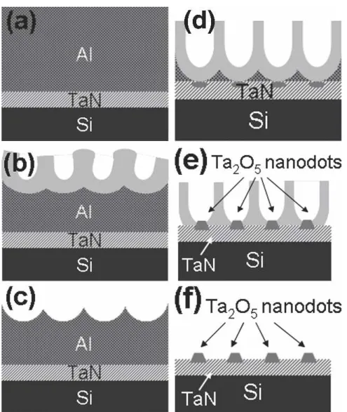
A schematic illustration of the microstructural evolu-tion for our AAO template synthesis is presented in Fig. 1. A multifunction sputtering system (ULVAC SBH-3308 RDE, Tokyo, Japan) was used to deposit TaN on p-type (100) 6-in. silicon wafer ( ⳱ 2 to 100 ⍀ cm). A gas mixture of Ar/N2(30:1.7) and Ta target of 99.999% were used to deposit 50-nm TaN for 224 s. A thermal evaporation coater (ULVAC EBX-6D) was utilized to grow 1.5-m Al (99.999%) on top of the TaN layer [Fig. 1(a)]. The wafer was then broken into pieces for anodi-zation treatment. Each piece (∼1.8 cm2
) was treated with a two-step anodization process25
to form an ordered tan-talum oxide nanostructure. The first step of anodization was carried out in 0.3 M oxalic acid (H2C2O4) at a
con-pletely, oxygen may have diffused into the TaN film and oxidized part of the TaN film into Ta2O5 nanodots, as illustrated by Figs. 1(d) and 1(e). Afterward, the AAO film was selectively removed by a solution of 6.0 wt% phosphoric acid, 1.8 wt% chromic acid, and 92.2 wt% water. The partial anodization of TaN was confined within the AAO pores to form the nanodot structure. The chemical composition of the tantalum oxide nanodots was determined by x-ray photoelectron spectroscopy (XPS) using a PHI 1600 ESCA (Physical Electronics, Chanhassen, MN) system with Mg K␣(1253.60 eV) x-ray radiation at a power of 300 W. The pressure during analysis was 5 × 10⁻⁹Torr. The photoelectron take-off angle was set at 90°. The value of binding energy was referenced to that of the C 1s peak at 284.6 eV. The morphology of the tantalum oxide nanodots was charac-terized by field emission scanning electron microscope (FESEM; JSM-6500F, JOEL, Tokyo, Japan) and trans-mission electron microscope (TEM; JEM-2010, JOEL, Tokyo, Japan). Glancing angle x-ray diffraction (XRD) (Rigaku D/max-3C, Tokyo, Japan) was used for phase identification of the tantalum oxide nanodots. The Cu K␣ line of 1.54 Å was used for a range of 2 ⳱ 20° to 60°, and the recorded diffraction peaks were compared with standard JCPDS database for phase confirmation.
III. RESULTS AND DISCUSSION
Figure 2 provides the relation for current density ver-sus time in our two-step anodization treatments. One-and-a-half micrometers Al were deposited on top of 0.05m TaN on a Si substrate. Anodization of Al results in formation of AAO, accompanied by a height incre-ment of 120%.26Assuming a 100% coulomb efficiency, the AAO template can be designed by adjusting the amount of charge during first and anodization process second.
As shown in Fig. 2(a), anodization of blank 1.5-m Al on Si substrate was performed to measure the necessary time for complete reaction of Al. Under constant voltage of 40 V, there were initially instabilities in current, re-sponse but within 60 s, a steady current density of 20 mA/cm2
drastically when Al was entirely consumed. The plateau of 20 mA/cm2suggests it took 575 s to react 1.5-m Al. Figure 2(b) is the i-t curve for the first anodization step. As shown, we terminated the first anodization after 275 s, hoping to consume 0.75-m of Al in the process. After removing the irregular AAO, in the second anodization we converted the remaining 0.75-m of Al into AAO. The formation of AAO was evidenced by a duration of 275 s in a 20 mA/cm2plateau, as shown in Fig. 2(c). At the end of the second anodization, the current density dropped to 2 mA/cm2
when the barrier layer of AAO was broken through and TaN started reacting to form tanta-lum oxide. The duration of tantatanta-lum oxide formation was 50 s. The sharp drop in current density during nanodot formation reflects the resistive nature of TaN (200– 5000 ⍀ cm) versus Al (2.7–3.2 ⍀ cm). The same two-step anodization treatment was used by Chen et al. in
the Al–TiN system in which a similar drop in current was reported when TiN started reacting to form TiO2at the end of the second anodization.24
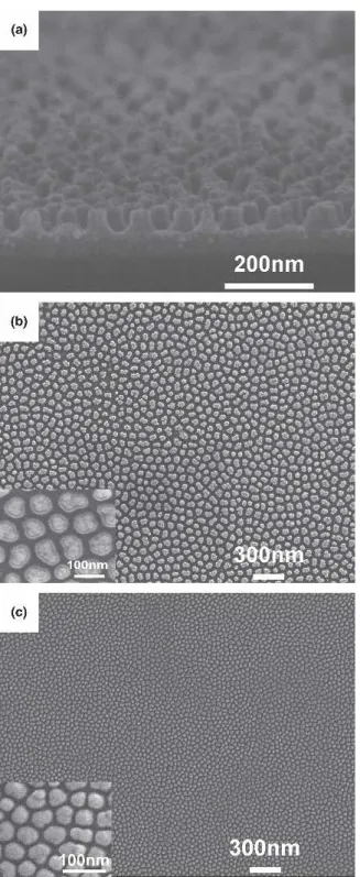
Figures 3(a) and 3(b) present the cross-sectional and top-view images from FESEM on tantalum oxide nano-dots after the AAO template was removed by the end of the second anodization step. Chemical removal of AAO was achieved in a solution of 6.0 wt% phosphoric acid (H3PO4) and 1.8 wt% chromic acid (H2Cr2O4) at 60 °C for 40 min. It can be seen that each individual tantalum oxide nanodot exhibited a hillock structure 80 nm in diameter on the bottom and 50 nm in height. It should be noted that the diameter of the nanodot bottom is identical to that of the AAO pore, and the arrangement of the nanodots replicates the precise pattern of the AAO tem-plate. This suggests that each nanodot was developed from the bottom of an individual AAO pore during
FIG. 1. Schematic diagrams showing the steps involved in fabrication of ordered Ta2O5nanodots: (a) deposition of 50-nm TaN and 1.5-m Al
on a p-type Si substrate, (b) first anodization step to form irregular AAO layer, (c) chemical etching to remove the freshly formed AAO layer with surface nanoindents left, (d) second anodization step to grow ordered AAO and oxidation of TaN to form Ta2O5at the pore bottom, (e) formation
anodization. Figure 3(c) displays the top-view FESEM image of the nanodot structure fabricated under different anodization parameters, i.e., 10 °C at constant voltage of 25V and 0.3 M sulfuric acid. As shown in Fig. 3(c), the resulting diameter of the tantalum oxide nanodot is ap-proximately 30 nm. This demonstrates the general appli-cability of the AAO template method in synthesizing nanodots of specific dimensions by controlling the pore formation electrochemistry in Al anodization.
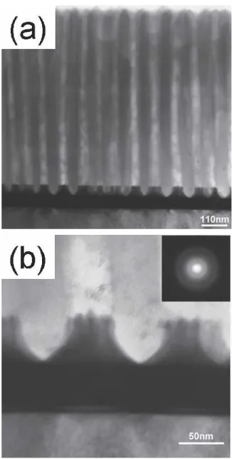
Figures 4(a) and 4(b) present the cross-sectional TEM images of the remaining AAO nanopores after the second anodization process. From Fig. 4(a), we confirm that AAO channels are parallel to each other and stay per-pendicular to the bottom. Figure 4(b) is a high-magnification view of the AAO pore bottom. The
FIG. 2. Typical i-t responses from two-step anodization treatment: (a) 1.5-m Al/Si substrate, (b) first step anodization of Al/TaN/Si substrate, and (c) second step anodization of Al/TaN/Si substrate.
FIG. 3. (a) Cross-sectional FESEM image of patterned Ta2O5nanodots
after AAO removal, (b) top-view FESEM image of Ta2O5nanodots
showing a diameter of 80 nm, and (c) top-view FESEM of Ta2O5
diffraction pattern of the Ta2O5nanodots is also shown in Fig. 4, which indicates that the nanodots are amorphous. The hillock nanodots are clearly seen extending from the underlying TaN layer.
The height of the AAO template in Fig. 4(a) was meas-ured at 0.80 m. Taking into account the 120% height expansion in AAO formation, the Al layer remaining after the first anodization is approximately 0.69m. This suggests that the Al layer of 0.81 m was consumed in the first anodization process. These numbers agree rea-sonably with Figs. 2(b) and 2(c); 0.75-m Al was used in the first anodization, and 0.75-m Al remained for the second anodization.
Glancing angle XRD was conducted to confirm the phase and composition of the surface film. Figure 5(a)
presents the diffraction pattern of the silicon substrate after TaN coating prior to Al deposition. The as-deposited TaN film demonstrates a crystalline phase with (111) and (200) planes clearly identified. This is ex-pected because the TaN deposition was conducted fol-lowing established semiconductor processing protocols at the National Nanodevice Laboratory where crystalline and conductive TaN is used as diffusion barrier for Cu damascence process. The resistivity of the TaN should be 200–5000 ⍀ cm. Figure 5(b) exhibits the diffraction pattern of tantalum oxide with AAO layer removed after completion of the second anodization step. The diffrac-tion pattern does not present a distinguishable peak, only amorphous characteristics. Thus, we conclude that the phase of as-prepared tantalum oxide is amorphous.
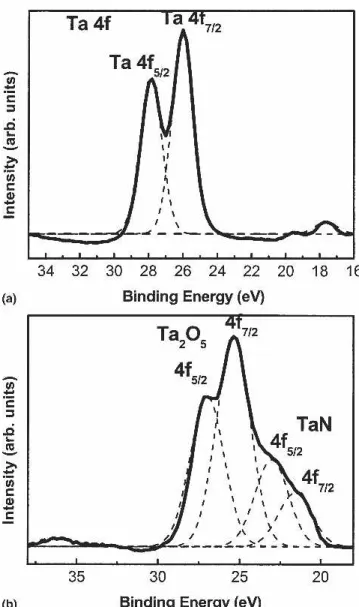
XPS was performed to investigate the chemical com-position of tantalum oxide because the com-position and shape of the photoelectron signals reflect the exact nature of electronic configuration. Figure 6(a) shows the XPS results of tantalum oxide nanodots. The specimen was presputtered for 10 s for sample cleaning. Because of the spin quantum orbital and electron configuration, l s cou-pling would take place and degenerate the orbital (angu-lar momentum >0) into two energy levels, as shown in Fig. 6(a). The intensities of these two peaks presented in Fig. 6(a) are 42321:32600 ⳱ 100:77, respectively. The ratio of these two peaks is 4:3, confirming the f-orbital characteristic of the Ta ion. Shift of those two peaks into higher binding energy is also observed, which is attrib-uted to the effect of chemical shift perturbation. The precise XPS signals require calibration by carbon. The position of C (1s) was 288.5 eV. This value exhibits an offset of +4.0 eV. After taking this into consideration, the positions of the XPS peaks should be 27.85 and 25.99 eV, instead. These values agree nicely with what would be expected from Ta5+ 4f5/2(27.85 eV) and 4f7/2
FIG. 5. Glancing angle XRD results of (a) TaN film showing a crys-talline phase with (111) and (200) indexed, and (b) Ta2O5nanodots
showing an amorphous characteristic.
FIG. 4. Cross-sectional TEM images of (a) AAO pore channel show-ing a pore diameter of 80 nm and pore height of 800 nm, and (b) pore bottom showing a hillock structure of Ta2O5nanodot.
(25.99eV).27,28Moreover, for chemical composition con-firmation, it is necessary to ensure that relative position of these two peaks is in proper order. In theory, Ta5+4f5/2 and Ta5+4f7/2 peaks should demonstrate a difference of 1.91 eV.27 As expected, these two peaks exhibit a dif-ference of 1.86 eV. Because of almost identical relative positions, we conclude with confidence that the peaks displayed in Fig. 6(a) were from Ta2O5signals, confirm-ing the existence of stoichmetric Ta2O5 nanodots.
Sputter depth profile analysis was used to measure the Ta5+ signal in the film and record the variation of TaN layer after the two-step anodization process. Figure 6(b) displays the XPS result after 60 s of sputtering. In con-trast with the results shown in Fig. 6(a), peaks associated with Ta2O5 became less distinct. Further, additional peaks at low binding energy were clearly present. Fol-lowing the carbon calibration mentioned above, these peaks were identified as 4f5/227.00 eV, 4f7/2 25.40 eV,
in-diffusion. Nevertheless, localized high field at the AAO pore bottom was expected to accelerate diffusion for Ta5+ions, facilitating the formation of hillock struc-ture.21,26We believe our Ta2O5nanodots were formed in following sequence. The O2−ions migrated through the AAO barrier layer and reacted with Ta5+ at the TaN/ AAO interface to form the inner part of Ta2O5nanodots. In addition, Al–O bonds in AAO barrier layer were de-stroyed by the strong electric field and Ta5+ diffused toward the AAO barrier layer and combined with O2− ions in the AAO layer, forming the top portion of Ta2O5 nanodots. The volume expansion associated with trans-formation of TaN to Ta2O5 promoted the formation of hillocks, as observed in FESEM pictures.
Calculation of transport number26,29
was conducted to provide insight on the formation kinetics of Ta2O5 na-nodots. Assuming the migrations of Ta5+
and O2− ions are totally responsible for the measured current, the fol-lowing equations can be applied during anodization proc-ess:
冉
␣dh + dt + dh− dt冊
= jfMTa zFK , (1) 26,29 TTa5+= ␣dh + dt ␣dh + dt + dh− dt , (2)26 TO2−= dh− dt ␣dh + dt + dh− dt , (3)26where (density of Ta2O5)⳱ 8 × 10³kg/m3, jf(current density in Ta2O5formation)⳱ 2 mA/cm
2
, MTa(atomic weight) ⳱ 181 g/mol, F ⳱ 96500 coulomb, z ⳱ 5, K(constant) ⳱ MTa/MTaO ⳱ 0.82,
26
h+ ⳱ height of Ta2O5, h
− ⳱ the depth of diffusion beneath the AAO/ TaN interface,␣ ⳱ porosity of the Ta2O5, TTa5+⳱ trans-port number of Ta5+
, and TO2− ⳱ transport number of
FIG. 6. XPS results of (a) Ta2O5nanodots after presputtering of 10 s,
O2−. From TEM pictures, we determined that h+⳱ 53 nm, h−⳱ 37 nm, and porosity ⳱ Nr2⳱ 0.38 (N is the number of pores per unit surface area and the pore diam-eter is equal to 2r). In addition, the formation time of Ta2O5was 50 s, as determined by Fig. 2. From the above discussion, we obtained h+ /t ⳱ 1.06 × 10− 9 , h− /t⳱ 0.74 × 10⁻⁹ , and␣h+ /t⳱ 0.403 × 10⁻⁹ . Inserting these values into Eqs. (2) and (3) we arrive at TTa5+ ⳱ 0.36 and TO2−⳱ 0.64.
Previous study of anodization of Ta to form amor-phous Ta2O5thin film showed a range of TTa5+from 0.18 to 0.32,30,31following a linear dependence with electric-field strength (MV/cm). Since the formation of AAO structure promotes field concentration at the pore bottom, it is expected that Ta diffusion would be accelerated resulting in higher TTa5+. In addition, amorphous nano-dot of Ta2O5is likely to offer facile diffusion paths for Ta5+as compared to those from defect-free Ta2O5film. Indeed, Vorobyova and Outkina also reported TTa5+ ⳱ 0.4 for binary Ta/Al film structure.26 This is in accord with our argument that enhanced field strength at the AAO pore bottom accelerates the slow-moving Ta5+.
Mozalev et al. have reported detailed experiments us-ing Al–Ta (1.1 m Al/300 nm Ta) binary films on Si substrate to prepare tantala columns (200–300 nm) within AAO structure.20,21 They conducted a two-step anodization in which each step is composed of galvano-static and potentiogalvano-static combination. Nucleation of the tantala hillock was observed at the end of first anodiza-tion in potentiostatic voltage of 50 V. Growth of hillocks into the tantalum oxide column was carried out by sec-ond anodization where voltage as high as 300 V was used. In contrast, our two-step anodization is relatively straightforward as identical potentiostatic teatments of 40 V were imposed. In addition, our 50-nm TaN is rather thin, and the hillock tantalum oxide we observed is still in the nucleation state as suggested by Mozalev et al.20In short, our approach provides a much simpler way to form tantalum oxide via an AAO template.
IV. CONCLUSIONS
Films of TaN (50 nm) and Al (1.5m) were deposited sequentially onto a p-type silicon substrate for a two-step anodization treatment in which amorphous Ta2O5 nano-dots were fabricated using in situ formed AAO as a tem-plate to promote localized anodization of TaN at the AAO pore bottom. The Ta2O5nanodots exhibited a hill-ock structure 80 nm in diameter at bottom and 50 nm in height. XPS results confirmed the chemical identity of Ta2O5. XRD data demonstrated the amorphous nature of the nanodots. Transport number calculation showed en-hanced diffusion of Ta5+
under the high electric field experienced in anodization. In addition, the arrangement and size of the nanodots replicate the AAO template. In
summary, this method provides a simple approach in synthesizing patterned oxide nanodots using binary Al and TaN films.
ACKNOWLEDGMENTS
The authors would like to thank the National Science Council of the Republic of China for financial support. Technical support from the National Nano Device Labo-ratories is gratefully acknowledged.
REFERENCES
1. S-H. Jeong, H-Y. Hwang, K-H. Lee, and Y. Jeong: Template-based carbon nanotubes and their application to a field emitter.
Appl. Phys. Lett. 78, 2052 (2001).
2. P-L. Chen, W-J. Huang, J-K. Chang, C-T. Kuo, and F-M. Pan: Fabrication and field emission characteristics of highly ordered titanium oxide nanodot arrays. electrochem. Solid-State Lett. 8, H83 (2005).
3. P-L. Chen, C-T. Kuo, F-M. Pan, and T-G. Tsai: Preparation and phase transformation of highly ordered TiO2nanodot arrays on
sapphire substrates. Appl. Phys. Lett. 84, 3888 (2004).
4. L.C. Tien, P.W. Sadik, D.P. Norton, L.F. Voss, S.J. Pearton, H.T. Wang, B.S. Kang, F. Ren, J. Jun, and J. Lin: Hydrogen sensing at room temperature with Pt-coated ZnO thin films and nanorods. Appl. Phys. Lett. 87, 2221061 (2005).
5. G. Jin, J.L. Liu, S.G. Thomas, Y.H. Luo, K.L. Wang, and B-Y. Nguyen: Controlled arrangement of self-organized Ge is-lands on patterned Si (001) substrates. Appl. Phys. Lett. 75, 2752 (1999).
6. T. Kitajima, B. Liu, and S.R. Leone: Two-dimensional periodic alignment of self-assembled Ge islands on patterned Si(001) . . . surfaces. Appl. Phys. Lett. 80, 497 (2002).
7. X. Mei, D. Kim, H.E. Ruda, and Q.X. Guo: Molecular-beam epitaxial growth of GaAs and InGaAs/GaAs nanodot arrays using anodic Al2O3nanohole array template masks. Appl. Phys. Lett. 81,
361 (2002).
8. H. Masuda, K. Yasui, and K. Nishio: Fabrication of ordered arrays of multiple nanodots using anodic porous alumina as an evapora-tion mask. Adv. Mater. 12, 1031 (2000).
9. A.P. Li, F. Müller, A. Birner, K. Nielsch, and U. Gösele: Hex-agonal pore arrays with a 50–420 nm interpore distance formed by self-organization in anodic alumina. J. Appl. Phys. 84, 6023 (1998).
10. J. Liang, H. Chik, A. Yin, and J. Xu: Two-dimensional lateral superlattices of nanostructures: Nonlithographic formation by an-odic membrane template. J. Appl. Phys. 91, 2544 (2002). 11. D. Crouse, Y-H. Lo, A.E. Miller, and M. Crouse: Self-ordered
pore structure of anodized aluminum on silicon and pattern trans-fer. Appl. Phys. Lett. 76, 49 (2000).
12. S. Shingubara, O. Okino, Y. Murakami, H. Sakaue, and T. Takahagi: Fabrication of nanohole array on Si using self-organized porous alumina mask. J. Vac. Sci. Technol. B 19, 1901 (2001). 13. T. Iwasaki, T. Motoi, and T. Den: Multiwalled carbon nanotubes
growth in anodic alumina nanoholes. Appl. Phys. Lett. 75, 2044 (1999).
14. W. Hu, D. Gong, Z. Chen, L. Yuan, K. Saito, C.A. Grimes, and P. Kichambare: Growth of well-aligned carbon nanotube arrays on silicon substrates using porous alumina film as a nanotemplate.
Appl. Phys. Lett. 79, 3083 (2001).
nuclear microanalysis. J. Electrochem. Soc. 130, 1267 (1980). 20. A. Mozalev, M. Sakairi, I. Saeki, and H. Takahashi: Structure,
morphology, and dielectric properties of nanocomposite oxide films formed by anodizing of sputter-deposited Ta–Al bilayers.
J. Electrochem. Soc. 151, F257 (2004).
21. A. Mozalev, M. Sakairi, I. Saeki, and H. Takahashi: Nucleation and growth of the nanostructured anodic oxides on tantalum and niobium under the porous alumina film. Electrochim. Acta 48, 3155 (2003).
22. S.Z. Chu, S. Inoue, K. Wada, S. Hishita, and K. Kurashima: A new electrochemical lithography-fabrication of self-organized
ti-28. Y. Masuda, S. Wakamatsu, and K. Koumoto: Site-selective depo-sition and micropatterning of tantalum oxide thin films using a monolayer. J. Eur. Ceram. Soc. 24, 301 (2004).
29. H. Takahashi and M. Nagayama: The determination of the poros-ity of anodic oxide films on aluminium by the pore-filling method.
Corros. Sci. 18, 911 (1978).
30. Q. Lu, P. Skeldon, G.E. Thompson, D. Masheder, H. Habazaki, and K. Shimizu: Transport numbers of metal and oxygen species in anodic tantala. Corros. Sci. 46, 2817 (2004).
31. J.P.S. Pringle: The anodic oxidation of superimposed metallic layers: Theory. Electrochim. Acta. 25, 1423 (1980).