行政院國家科學委員會專題研究計畫 成果報告
高性能長壽命可撓式有機薄膜電晶體元件之製作與研究 (II)
研究成果報告(精簡版)
計 畫 類 別 : 個別型
計 畫 編 號 : NSC 97-2221-E-011-135-
執 行 期 間 : 97 年 08 月 01 日至 98 年 07 月 31 日 執 行 單 位 : 國立臺灣科技大學電子工程系
計 畫 主 持 人 : 范慶麟
報 告 附 件 : 出席國際會議研究心得報告及發表論文
處 理 方 式 : 本計畫涉及專利或其他智慧財產權,2 年後可公開查詢
中 華 民 國 98 年 10 月 14 日
高性能長壽命可撓式有機薄膜電晶體元件之製作與研究(II)
“Investigation and fabrication of flexible organic thin film transistor devices with high performance and long lifetime (II)”
計畫編號:NSC97-2221-E-011-135
執行期間:97 年 08 月 01 日 至 98 年 07 月 31 日 主持人:范慶麟 台灣科技大學電子工程系副教授
I. 中文摘要
本計劃利用 NH3電漿針對有機薄膜電晶體
(OTFTs)之 SiO2閘極絕緣層進行表面處理,研究 結 果 顯 示 NH3 電 漿 處 理 技 術 可 改 善 SiO2/pentacene 之間的介面品質,提供一個適當 的表面讓有機主動層材料 pentacene 成長。此 外,藉由NH3電漿處理技術也可幫助鈍化SiO2
閘極絕緣層表面的懸浮鍵,進而降低表面的缺
陷狀態密度。因此我們所提出的 NH3電漿處理
是一個簡單且有效的表面處理技術,它不但可
以降低 SiO2閘極絕緣層的表面缺陷密度,且同
時改善了pentacene 的結晶品質。
關鍵字:有機薄膜電晶體、pentacene、NH3 電 漿、閘極絕緣層處理、載子移動率、介面缺陷 狀態密度。
Abstract
This study examined the effects of NH3-plasma treatment on the gate insulator (SiO2) surface before pentacene deposition. The NH3-plasma treatment can improve the interface property between SiO2/pentacene, providing a suitable surface for pentacene growth. Moreover, the NH3-plasma treatment can also help terminate dangling bonds at the SiO2 surface and thus reduce the interface trap-state density. The proposed method provides a simple and effective method for treating the interface between SiO2/pentacene, reducing interface traps and
simultaneously improving pentacene crystallization.
Keywords: organic thin film transistor, pentacene, NH3-plasma, gate insulator treatment, interface trap-state density.
II. INTORDUCTION
Organic thin-film transistors (OTFTs) have attracted much attention due to their low-temperature and low-cost fabrication process.
They have great potential for application to novel, low-cost and large-area flexible electronics. Their possible applications are flat-panel displays, electronic papers and radio-frequency identification tags (RFIDs), etc. [1–3]. OTFT performance has been significantly improved in the last few years and is comparable to that of the amorphous silicon thin-film transistors (a-TFTs) with process parameter optimization [4–6].
Because most organic active materials, such as pentacene (C22H14) are hydrophobic, the hydrophilic inorganic gate insulators, for example silicon dioxide (SiO2), are unsuitable for growing pentacene to form polycrystalline due to the high surface potential energy [7]. In order to improve the pentacene growth property, various techniques have been proposed to improve the interface property and reduce surface potential energy
between the inorganic SiO2 gate insulator and organic pentacene active layers [7–10]. The self-assembled monolayer (SAM), such as
hexamethyldislane (HDMS) or octadecyltrichlorosilan (OTS), was used to greatly
reduce the surface potential energy and thus improve the interface properties. The SAM process can improve the pentacene growth property, but it is a wet process and the inorganic SiO2 OTFT gate insulator requires immersion in SAM solution for a long time, such as 24 h.
Sometimes, the long immersion time may remove the contact metals and the solvent used in SAM process may attack the plastic substrate employed for the flexible display.
It has also been reported that interface trap-states, such as dangling bonds or weaker bonds, between the SiO2 gate insulator and pentacene active layers are also key issues that affect OTFT performance [11–13]. Some schemes have been used to reduce the interface trap-states to improve pentacene-based OTFT performance [14,15]. In this study, we propose using an NH3-plasma treatment to improve the interface property between the SiO2 and pentacene and simultaneously reduce the interface trap-states, resulting in performance improvement. We believe that the proposed NH3-plasma treatment is a good candidate to effectively improve OTFT performance.
Fig. 1. Schematic diagram of pentacene-based OTFTs with bottom-contact configuration.
III. EXPERIMENT
The bottom-contact (BC) configuration of pentacene-based OTFTs were fabricated onto a highly doped n-type Si wafer (resistivity < 0.020 ohm cm, 500 lm-thick) acting as the gate electrodes. The pentacene-based OTFT configuration is shown in Fig. 1. Thermally grown 100 nm-thick SiO2 was used as the gate insulator and the Cr/Pt (2 nm/70 nm) were evaporated using an Electron-Beam evaporation system as source/drain (S/D) electrodes. The lift-off method was used to pattern the electrodes onto the SiO2. High density plasma chemical vapor deposition (HDP-CVD) NH3-plasma was conducted before pentacene deposition to treat the SiO2/pentacene interface. The inductively coupled plasma (ICP) power of HDP-CVD was 100 W. The chamber pressure was 30 mTorr and the gas flow rate 100 sccm. The gas composition of the NH3-plasma was pure NH3 gas. The plasma exposure time was 30 min. Additionally to avoid large surface roughness in the gate insulator which degrades device performance, the plasma treatment time and plasma power should be considered at the same time as a result of the slighter etching effect.
After the NH3-plasma treatment, the pentacene purchased from Sigma Aldrich (without any purification) was deposited onto the SiO2 as the active layer material. The substrate temperature was kept at 70 ℃. Pentacene film at a thickness of 100 nm was deposited at a rate of 0.1–0.3 Å/s. The device’s channel width (W) and channel length (L) were around 500 and 4 μm, respectively. The devices were stored and measured at room temperature in atmosphere. The surface morphology and grain size of the pentacene film, as the active layer, were observed using atomic force microscopy (AFM). The contact angle
measurement system (FTA 1000B, First Ten Angstroms, Inc.) was used to analyze the contact angle and surface potential energy. De-ionized water, glycerol and di-iodomethane were employed as the testing liquids. The electrical measurement was performed using an Agilent HP 4156A semiconductor parameter analyzer in the dark at room temperature.
IV. RESULTS and DISCUSSION
The surface morphology of pentacene films with and without NH3-plasma treatment were investigated using AFM, as shown in Fig. 2a and b, respectively. The average grain size of the pentacene film with NH3-plasma treatment (about 2.40 μm) was larger than that without treatment (about 1.98 μm). The standard deviation of average grain size with and without NH3-plasma treatment was 0.90 and 0.96, respectively. This difference in grain size is presumed to be due to the following reasons. First, the reduction of surface potential energy is believed to result in the large grain size [16]. It has been reported that the plasma treatment can reduce the surface potential energy barrier because the contaminants on the surface of the gate insulator are removed by plasma and thus provide a large diffusion length for forming large polycrystalline grain [7,10,17].
The contact angle and surface potential energy measurement results are shown in Table 1. The surface energy was calculated using the Girifalco–Good–Fowkes–Young (GGFY) model [18]. It indicated that the surface potential energy after NH3-plasma treatment decreased from 53.66 to 47.66 mN/m. AFM images of the SiO2 surface with and without NH3-plasma treatments are shown in Fig. 3. The roughness values for the
SiO2 surface with and without NH3-plasma treatment were 0.743 and 0.285 nm, respectively.
Fig. 2. The AFM images of pentacene film (a) with and (b) without NH3-plasma treatment onto the SiO2 surface.
We presumed the SiO2 surface was cleaned using NH3-plasma because of the slight etching on the surface, resulting in increased SiO2 surface roughness. We believe that the NH3-plasma treatment can clean the SiO2 surface, resulting in decreased surface potential energy. Second, the formation of a hydrophobic SiO2 surface can improve improve the crystallinity of the grown pentacene [3,5,7,8]. It is well known that SiO2 is a porous material and usually includes hydrophilic OH or H bonds in its network. These OH or H bonds produce SiO2 with hydrophilic
characteristics [7].
Table 1
Comparison of the contact angles and surface potential energies of gate insulator (SiO2) with and without NH3-plasma treatment, respectively.
Fig. 3. The AFM images of SiO2 surface (a) with and (b) without NH3-plasma treatment.
These hydrophilic bonds may result in inferior crystallinity in the grown pentacene film. Fig. 4 shows the contact angle measurement results, which employed de-ionized water as the analytic solution to analyze the SiO2 surface properties with and without NH3-plasma treatment. It indicated that after NH3-plasma treatment, the contact angle increased from 28.71°to 47.14°. It has been reported that hydrogen radicals dissociated from NH3-plasma will react with OH
Fig. 4. The contact angles of SiO2 surface (a) with and (b) without NH3-plasma treatment.
and H bonds to form H2O and H2 which can diffuse outward from the SiO2 network [17].Thus, it is presumed that the surface property of the SiO2
was changed from hydrophilic to hydrophobic characteristics, that as a result of the dissociated hydrogen radicals from NH3-plasma reacting with these hydrophilic bonds. We believe that the hydrogen radicals dissociated from NH3-plasma resulted in the SiO2 hydrophobic surface to improve the crystallinity of the grown pentacene thin-film. The pentacene film with improved crystallinity will have large and uniform grains, as shown in Fig. 2a. The large and uniform grains can decrease the carrier scattering during carrier transport to result in good device performance.
The small and non-uniform grains tend to have voids, resulting in the carrier transport through this material significantly degraded by the voids [19]. Fig. 5a and b shows the typical output curves (IDS–VDS) for the pentacene-based OTFTs with and without NH3-plasma treatment, respectively.
It was found that the saturation drain current (IDS) of pentacene-based OTFTs with NH3-plasma treatment is larger than that without NH3-plasma
treatment. Fig. 6 shows the typical transfer curves (IDS–VGS) for the pentacene-based OTFTs with and without NH3-plasma treatment. The device electrical parameters are summarized in Table 2.
The field-effect mobility (μFE) of pentacene-based OTFTs was estimated from plotting Eq. (1) for the saturation region:
2 TH GS i FE )
DS( (V V )
L C
I sat =Wμ −
(1) where IDS is the source–drain current, VGS the source–gate voltages, VDS the source–drain voltages, VTH the threshold voltage, W and L the channel width and length, Ci the gate insulator capacitance (per unit area), respectively. It was noted that the improvement percentage of μFE, and ON/OFF current ratio (ION/IOFF) of pentacene-based OTFTs with NH3-plasma treatment were 242.8% and 732%, respectively.
The improvement is more obvious and significant than that of the reported papers [7,15,20]. It was found that NH3-plasma treatment before pentacene deposition can significantly improve the electrical characteristics of the pentacene-based OTFTs, especially in mobility and on-current. The NH3-plasma treatment causes the low surface potential energy of the SiO2 surface and the hydrophobic SiO2 surface, and thus increases in pentacene grain size, decreases in the grain boundaries, and improved OTFT turn-on performance. In addition, it had been reported that the off-current was dominantly determined by the interface state between the pentacene active layer and SiO2 surface [14,15]. These traps would cause the carriers existing in the channel, making it
Fig. 5. Typical output curves (IDS–VDS) of the pentacene-based OTFTs (a) with and (b) without NH3-plasma treatment.
Fig. 6. Typical transfer curves (IDS–VGS) of the pentacene-based OTFTs with and without NH3-plasma treatment, respectively.
Table 2
Device characteristics comparison for pentacene-based TFTs with and without NH3-plasma treatment, respectively.
difficult to repel the carriers in the traps with the gate voltage. When devices without treatment were operated in the off state, the drain current could not be effectively turned off [15]. The interface trap values are also listed in Table 2. We estimated and extracted the interface trap density in the devices using the methods of Levinson et al.
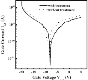
[21] and Cristoloveanu et al. [22]. It was found that there is a 36% decrease in the interface traps for NH3-plasma treatment devices. The gate insulator (SiO2) leakage current with and without plasma treatment is shown in Fig. 7.
Fig. 7. The gate leakage current (IGS–VGS) of the pentacene-based OTFTs with and without NH3-plasma treatment, respectively
It indicates that the NH3-plasma treatment can decrease the gate insulator (SiO2) leakage current.
Thus, we presumed that the nitrogen radicals dissociated from the NH3-plasma can help terminate the dangling bonds between the SiO2
and pentacene to form strong Si–N bonds, resulting in the reduction in defect states and performance improvement for pentacene-based
OTFTs [23,24]. We believe that the improvement in sub-threshold swing of the treated devices resulted from the decreased defect states and interface trap-state density between the SiO2 and pentacene interface. Additionally, it has been reported [20,25] that hydrogen radicals dissociated from NH3 treatment could increase the electron trapping to result in the produced built-in negative gate voltage. Thus, the threshold voltage of OTFTs with NH3-plasma treatment can be decreased and the OTFTs can be turned on early.
In summary, the hydrogen radicals dissociated from NH3-plasma can improve the crystallinity, resulting in the formation of a hydrophobic SiO2
surface. This produces improved mobility and on-current characteristics in pentacene-based OTFTs. The experimental results exhibit that the improvement percentage of mobility and on-current were 242.8% and 148.5%, respectively.
In addition, the nitrogen radicals dissociated from NH3-plasma can reduce the dangling bonds and decrease the interface traps-state density between the SiO2 and pentacene, producing performance improvement in pentacene-based OTFTs, especially in the off-current state. The experimental results exhibit that the improvement percentage of off-current state was 70%.
V. CONCLUSION
NH3-plasma treatment has been demonstrated to enhance the interface property between SiO2/pentacene and improve the electrical characteristics of pentacene-based OTFTs. The
NH3-plasma treatment can change the surface property of SiO2 into the hydrophobic state and thus reduce the surface potential energy and increasing the pentacene grain size, resulting in improved OTFT turn-on performance.
Furthermore, NH3-plasma can also produce nitrogen radicals to passivate the SiO2 layer, resulting from the termination of dangling bonds, and thus reducing interface traps to improve the performance, especially in the off-current state.
VI. REFERENCES
[1] Chaâbane RB, Gamoudi M, Guillaud G. Dielectric properties of calixarene thin films in a large frequency range. Synth Met 1994;67:231.
[2] Guillaud G, Simon J, Germain JP.
Metallophthalocyanines Gas sensors, resistors and field effect transistors. Coord Chem Rev 1998;178–180:1433.
[3] Puigdollers J, Voz C, Martín I, Vetter M, Orpella A, Alcubilla R. Electrical characterization of pentacene thin-film transistors with polymeric gate dielectric.
Synth Met 2004;146:355.
[4] Shtein M, Mapel J, Benziger JB, Forrest SR. Effects of film morphology and gate dielectric surface preparation on the electrical characteristics of organic-vapor-phase-deposited pentacene thin-film transistors. Appl Phys Lett 2002;81:268.
[5] Knipp D, Street RA, Völkel A, Ho J. Pentacene thin film transistors on inorganic dielectrics: Morphology, structural properties, and electronic transport. J Appl Phys 2003;93:347.
[6] Kelley TW, Boardman LD, Dunbar TD, Muyres DV, Pellerite MJ, and Smith TP. High-performance OTFTs using surface-modified alumina dielectrics. J Phys Chem B 2003;107:5877.
[7] Lim SC, Kim SH, Lee JH, Kim MK, Kim DJ, and Zyung T. Surface-treatment effects on organic thin-film transistors. Synth Met 2005;148:75.
[8] Wu BT, Su YK, Tu ML, Wang AC, Chen YS, Chiou YZ, Chiou YT, Chu C H. Interface modification in organic thin film transistors. Jpn J Appl Phys 2005;44:2783.
[9] Panzer MJ, Newman CR, Frisbie CD. Low-voltage operation of a pentacene field-effect transistor with a polymer electrolyte gate dielectric. Appl Phys Lett 2005;86:103503.
[10] Lee MW, Song CK. Oxygen plasma effects on performance of pentacene thin film transistor. Jpn J
Appl Phys 2003;42:4218.
[11] Lang DV, Chi X, Siegrist T, Sergent AM, Ramirez AP.
Bias-dependent generation and quenching of defects in pentacene. Phys Rev Lett 2004;93:076601.
[12] Lang DV, Chi X, Siegrist T, Sergent AM, Ramirez AP.
Amorphouslike density of gap states in single-crystal pentacene. Phys Rev Lett 2004;93:086802.
[13] Podzorov V, Pudalov VM, Gershenson ME.
Field-effect transistors on rubrene single crystals with parylene gate insulator. Appl Phys Lett 2003;82:1739.
[14] McDowell M, Hill IG, McDermott JE, Bernasek SL, Schwartz J. Improved organic thin-film transistor performance using novel self-assembled monolayers.
Appl Phys Lett 2006;88:073505.
[15] Kang S, Jung S, Park J, Lee HJ, Yi M. Gate dielectric surface treatment techniques for organic thin film transistor. Microelectron Eng 2007;84:1503.
[16] Bruening M, Moons E, Cahen D, Shanzer A.
Controlling the work function of CdSe by chemisorption of benzoic acid derivatives and chemical etching. J Phys Chem 1995;99:8368.
[17] Zhou ZH, Aydil ES, Gottscho RA, Chabal YJ, Reif R.
Real-Time, In situ monitoring of room-temperature silicon surface cleaning using hydrogen and ammonia plasmas. J Electrochem Soc 1993;140:3316.
[18] Girifalco LA and Good RJ. A theory for the estimation of surface and interfacial energies. I.
derivation and application to interfacial tension. J Phys Chem 1957:61:904.
[19] Lin YY, Gundlach DJ, Nelson SF, Jackson TN.
Stacked pentacene layer organic thin-film transistors with improved characteristics. IEEE Electr Dev Lett 1997;18:606.
[20] Kwan MC, Cheng KH, Lai PT, Che CM. Improved carrier mobility for pentacene TFT by NH3 annealing of gate dielectric. Solid-State Electron 2007;51:55.
[21] Levinson J, Shepherd FR, Scanlon PJ, Westwood WD, Este G, Rider M. Conductivity behavior in polycrystalline semiconductor thin film transistors. J Appl Phys 1982;53:1193.
[22] Cristoloveanu S, Li SS. Electrical Characterization of Silicon-On-Insulator Materials and Devices. Boston:
Kluwer Academic Publishers;1995.
[23] Cheng HC, Wang FS, Huang CY. Effects of NH3
plasma passivation on N-channel polycrystalline silicon thin-film transistors. IEEE Trans Electr Dev 1997;44:64.
[24] Zeng X, Sun XW, Li J, Sin JKO. Improving reliability of poly-Si TFTs with channel layer and gate oxide passivated by NH3/N2O plasma. Microelectron Reliab 2004;44:435.
[25] Severi M, Impronta M. Charge trapping in thin nitrided SiO2 films. Appl Phys Lett 1987;51:1702.
VII. 計畫成果自評
本計畫利用NH3電漿處理技術改善SiO2/pentacene之介面品質,且降低了SiO2閘極絕緣層的表面 缺陷密度,且同時改善了有機主動層材料–pentacene結晶特性,以提高有機薄膜電晶體(OTFTs)元 件效能,與原計畫目的相符、並達成預期與目標,目前本計劃研究成果已投稿至國際期刊Solid-State Electronics並已被刊登(Vol.53, pp. 246-250, 2009.)。
可供推廣之研發成果資料表
□ 可申請專利 ■ 可技術移轉 日期:98 年 10 月 14 日
國科會補助計畫
計畫名稱:高性能長壽命可撓式有機薄膜電晶體元件之製作與研究 (II) 計畫主持人:范慶麟
計畫編號:NSC 97-2221-E-011-135 學門領域:微電子學門 技術/創作名稱 以NH3電漿處理有機薄膜電晶體之SiO2閘極絕緣層
發明人/創作人 范慶麟 中文:
本計劃利用 NH3電漿針對有機薄膜電晶體(OTFTs)之 SiO2閘極絕緣 層進行表面處理,研究結果顯示NH3電漿處理技術可改善SiO2/pentacene
之間的介面特性,提供一個適當表面讓有機主動層材料pentacene 成長。
此外,藉由 NH3電漿處理技術也可幫助鈍化SiO2閘極絕緣層表面的懸浮
鍵,進而降低的表面的缺陷狀態密度。因此我們所提出的 NH3 電漿處理
是一個簡單且有效的表面處理技術,它不但可以降低 SiO2閘極絕緣層的
表面缺陷密度,且同時改善了pentacene 的結晶品質。
技術說明 英文:
This study examined the effects of NH3-plasma treatment on the gate insulator (SiO2) surface before pentacene deposition. The NH3-plasma treatment can improve the interface property between SiO2/pentacene, providing a suitable surface for pentacene growth. Moreover, the NH3-plasma treatment can also help terminate dangling bonds at the SiO2 surface and thus reduce the interface trap-state density. The proposed method provides a simple and effective method for treating the interface between SiO2/pentacene, reducing interface traps and simultaneously improving pentacene crystallization.
可利用之產業 及 可開發之產品
1. 有機薄膜電晶體與低溫複晶矽薄膜電晶體。
2. 無線射頻標籤。
3. 大面積氣體感測器。
4. 主動驅動液晶顯示器。
5. 主動驅動有機電激發光顯示器。
技術特點
1. 利用 NH3電漿處理可改善SiO2/pentacene 之界面品質。
2. 利用 NH3電漿處理可降低元件的interface trap-state density。
3. 利用 NH3電漿處理可提高元件效能。
推廣及運用的價值
利用 NH3電漿處理技術改善 SiO2/pentacene 之介面品質,且降低了 SiO2
閘極絕緣層的表面缺陷密度,且同時改善了有機主動層材料–pentacene 結 晶特性,以提高有機薄膜電晶體(OTFTs)元件效能。
※ 1.每項研發成果請填寫一式二份,一份隨成果報告送繳本會,一份送 貴單位研發成果 推廣單位(如技術移轉中心)。
※ 2.本項研發成果若尚未申請專利,請勿揭露可申請專利之主要內容。
※ 3.本表若不敷使用,請自行影印使用。
出席國際學術會議心得報告
計畫編號 NSC 97-2221-E-011 -135
計畫名稱 高性能長壽命可撓式有機薄膜電晶體元件之製作與研究(II)
出國人員姓名
服務機關及職稱 楊宗憲/國立台灣科技大學 電子所/博士班研究生
會議時間地點 September 23-26, 2008;日本茨城縣筑波市
會議名稱 2008 International Conference on Solid State Devices and Materials (SSDM2008) 發表論文題目 Instability of Threshold Voltage under DC Drain Bias Stress in Pentacene-based
Organic Thin Film Transistors
一、參加會議經過
於 9 月 23 日早上 8:55,搭乘華航班機前往日本,並於日本時間下午 1:30 分抵達日 本東京成田機場,隨即前往飯店 check in 並放置行李,稍微休息後即前往會議地點筑波 市 Tsukuba International Congress Center,會中邀請到 Prof. Simon Sze 進行專題演講,題 目為 “Nanoelectronic Technology: Challenges in the 21st Century”,Prof. Simon Sze 提到許 多關於目前奈米科技研究發展情形與對於未來的影響,包含奈米製程、奈米探管等製程 技術與應用概況,儘管與自身研究領域不同,但仍然使我獲益不少,並產生許多研究構 想以應用在有機薄膜電晶體(Organic Thin Film Transistors, OTFTs)的研究上。
9 月 24 日之會議議程是由來自世界各地的專家與研究學者進行研究論文發表,而學 生主要參加的 session 為“OrganicMaterials Science, Device Physics, and Applications”,
此 section 與目前學生之研究題目相關,並聆聽多場演說,其中來自瑞士的 Bertram Batlogg 博士受邀進行專題演講,題目為“Organic Field Effect Devices : Physics and Materials”,
內容提到有關於有機場效電晶體(Organic Field-Effect-Transistors, OFETs)元件劣化的相關 物理機制,包含 Trap-state 的產生、量測與計算方法,此學生獲益良多,因此機制為 OTFTs 與 OFETs 效能能否提升與操作穩定性改善的重點之一,而在聆聽過此場演講後,對於元 件 Trap-state 產生的機制與計算方法讓我有更深入的了解,相信對未來在 OTFTs 元件特 性改善與理論分析上,一定會有相當大的幫助;接著有許多學者發表多篇有機發光二極 體(Organic Light Emitting Diodes, OLEDs)相關研究論文,其中 Masato Shakutsui 提出使用 Bilayer Structure 並加以適當的熱處理,可改善載子注入的平衡,進而提升元件的發光效 率。此外,Hiroshi Yamauchi 提出 OLED 與 ZnO 電晶體整合之主動式元件,此積體化元 件對於未來主動式 OLED 顯示器有相當高的應用性,目前國內也是許多研究團隊針對此 技術進行研究,也是本研究團隊未來努力的方向。
9 月 25 日之會議議程是亦是由專家與研究學者進行研究論文發表,學生並於早上 10:45 至 12:00 的場次發表研究論文,以口頭報告方式介紹本研究成果,並於下午 13:00 至 14:45 進行海報發表,會中來自日本島根大學(Shimane University)的土屋敏章教授與學 生針對 OTFTs 元件劣化的相關機制進行討論與意見交換,土屋敏章教授為 IEEE Fellow,
化機制。
9 月 26 日為會議的最後一天,會中邀請Tetsuo Tsutsui教授(Kyushu University)發表演 說,題目為“Material Design of Phenylenevinylene Oligomers for Organic Field-Effect Transistors”,內容以Phenylenevinylene Oligomers為基底,進行材料化學結構設計與合 成,並製作成OTFTs元件並比較不同化學結構之材料其元件電性,由於目前OTFTs元件主 要採用pentacene與P3HT作為主動層材料,但受限於有機材料易受水氣與氧氣侵入,導致 特性變差,因此發展高穩定性與高載子移動率的材料,亦是OTFTs研發的重要課題之一,
Tetsuo Tsutsui教授所合成之(CH3-OPV)材料其載子移動率可達 0.13 cm2/Vs,以與非晶矽 (α-Si)薄膜電晶體特性相去不遠。此外,來自韓國三星電子的Sangyoon Lee 博士發表
“Organic and Printed Devices for Large Area Electronics”,利用噴墨技術製作OLEDs與 OTFTs元件,以實現主動式有機平面顯示器面板,噴墨技術的優點在於不需使用黃光製 程及可定義出各層材料之區域,是大面積有機顯示器主要開發的技術之ㄧ,會中所提之 顯示面板為 4.4 吋、解析度為 192 × 64 單色面板,畫素電路為 2T1C的基本電路結構,其 OTFTs元件特性亦相當不錯,載子移動率可達 0.1 cm2/Vs、on/off ratio 可達 107,由於此 面板為三星電子所研發,以目前本實驗室的相關設備或許目前難以達成,不過我們相信 未來將會有相關產品問世,而如何提高元件特性與增加操作穩定性將是我們目前研究的 主要課題。
9 月 27 日早上於飯店 check out 後,隨即搭乘電車前往東京成田機場,並搭乘下午 14:15 分之華航班機回台灣,結束此次研討會之行程。
二、與會心得
此次前往日本參加SSDM2008 研討會,是學生第一次前往其他國家參加國際性研討
會,於研討會期間除了在相關專業領域有相當大的收穫之外,第一次以英文口頭報告以 及與其他國家的專家學者討論的經驗,讓我更敢以英文與他人交談,;此外,這次在日 本生活將近五天的期間,體驗到不同於台灣的生活,我充分感受到日本人民在服務態度 與生活環境維護的用心與努用,這可做為我們努力的目標。這次的行程讓我見識到不一 樣的人、事、物,不僅提升自己的專業知識上,也讓自己知道有哪些不足許要加強的地 方,我很珍惜此次難得的機會,讓我受益良多。