國 立 交 通 大 學
電機與控制工程研究所
碩 士 論 文
小面積&低功率數位化 2.5Gb/s 收發器
A Small Area Low Power 2.5Gb/s Transceiver
With Digitized Architecture
研 究 生:蕭匡良
指導教授:蘇朝琴 教授
小面積&低功率數位化 2.5Gb/s 收發器
A Small Area Low Power 2.5Gb/s Transceiver
With Digitized Architecture
研 究 生:蕭匡良 Student : Kuang-Liang Hsiao
指導教授:蘇朝琴 教授 Advisor : Chau-Chin Su
國 立 交 通 大 學
電機與控制工程研究所
碩士論文
A Thesis
Submitted to Department of Electrical and Control Engineering College of Electrical Engineering and Computer Science
National Chiao Tung University in partial Fulfillment of the Requirements
for the Degree of Master
in
Electrical and Control Engineering July 2006
Hsinchu, Taiwan, Republic of China
小面積&低功率數位化 2.5Gb/s 收發器
研究生 : 蕭匡良 指導教授 : 蘇朝琴 教授
國立交通大學電機與控制工程研究所
摘 要
最近幾年,多媒體應用的蓬勃發展,製程技術不斷地演進,晶片上的處理速度越來越 快,資料處理量越來越多,網路的使用越來越便利,這伴隨著對於越來越高傳輸量的需求, 種種因素影響之下,在有限的通道(Channel) 傳輸越來越多的資料量變成一個不可避免的趨 勢,於是乎高速鏈結的傳輸技術研究亦自然地突顯出其重要性。 由於外來雜訊,如通道與通道間的交互影響(cross talk)或者電磁發散(EMI),阻抗的不匹配造成反射,以及通道本身會對訊號產生程度上的衰減,如 skin effect 與 Inter symbol
interference(ISI),另外非理想的傳輸端信號會有頻率與相位上的飄移,種種因素使得所以如 何達到高速而正確的傳輸,降低有限通道頻寬與外來雜訊的影響,進而接收到正確的資料 成為一個難以克服的問題。 在這我們採用數位化的10-1 多工器、1-10 解多工器、時脈資料恢復電路、接收器 前端電路和輸出驅動器並且和鎖相迴路整合成為一個完整的串列式資料收發器,此電路計 採用0.18um 1P6M TSMC CMOS 製程技術實現。 關鍵字: 收發器,時脈資料恢復電路,全數位化
A Small Area Low Power 2.5Gb/s Transceiver
With Digitize architecture
Student: Kuang-Liang Hsiao Advisor: Chau-Chin Su
Institute of Electrical and Control Engineering
National Chiao Tung University
Abstract
In recent years, the flourishing development of multimedia applications and the dimension scales down with the advance of IC fabrication technology, make the speed of IC operation getting higher. Accompanied with these higher demands for transmitting quantity transmitting in a limited channel becomes an unavoidable trend. Therefore, the high-speed transmission technical research naturally appears its importance.
However, because of outside noise such as the cross talk. Between channels or Electro
Magnetic Interference (EMI), reflection caused by the mismatch of impedance. The attenuation of
the signal which influenced by the channel itself, like skin effect and Inter Symbol Interference (ISI). Furthermore, frequency offset and phase wander of non-ideal transmission-end signals. These factors made how to reach a high speed and correct transmission, reduce influence of a limited channel and outside noise. And then receive correct data become a formidable problem.
In this thesis we implement a 10-to-1 serilaizer, 1-to-10 deserializer, clock and data recovery, receiver-front end, output driver circuit in digital approach. And integrate PLL together to become a serial link data transceiver it will be implemented using 0.18um 1P6M TSMC CMOS technology.
誌 謝
我想我最需要感謝的是我的家人,要是沒有他們在背後支持我,不會有今天 的我。 也要特別感謝我的指導教授 蘇朝琴 教授,老師不管在研究方面或生活處 事上,都讓我收穫很大,對於做事情的態度,老師一直是很積極的,因此在遇到 研究瓶頸時,我總是以積極的態度面對。 在此還要感謝一起在交大兩年多的同學們:冠宇(小冠)、宗諭(阿肉)、 智琦( Frank)、懋軒、順閔一起度過一星期 5 次 meeting 的碩二生活。另外還 有學弟們:賢哥、方董、教主、潘威祥、小馬、村鑫、祥哥、存遠,在我壓力大時, 大家一起亂哈拉幫我緩和情緒,特別感謝鴻文跟仁乾兩位博班學長總是在我最沒 靈感的時候,給我新 idea,另外丸子、煜輝學長、盈傑學長,史努比提供給我 最寶貴的經驗,沒有這些經驗,做起事來就不會那麼順利了。 蕭匡良 2006/9/5Table of Contents
TABLE OF CONTENTS --- V
LISTS OF FIGURES --- VII
LISTS OF TABLES--- IX
CHAPTER 1 INTRODUCTION --- 1
1.1MOTIVATION--- 1
1.2THESIS ORGANIZATION--- 3
CHAPTER 2 BACKGROUND STUDY --- 4
2.1BASIC SERIAL LINK--- 4
2.2TECHNIQUES OF TIMING RECOVERY--- 8
2.3TECHNIQUES OF SERIALIZER---13
CHAPTER 3 CLOCK AND DATA RECOVERY --- 16
3.1CDRTRACKING METHOD---16
3.2CDRARCHITECTURE---18
3.3BUILDING BLOCKS---19
3.4THE ANALYSIS OF CONFIDENCE COUNTER SIZE---25
3.5EXPERIMENTS---31
3.6SUMMARY---35
CHAPTER 4 2.5GB/S TRANSCEIVER WITH DIGITIZED
ARCHITECTURE --- 36
4.1INTRODUCTION OF TRANSCEIVER---36
4.2SHIFT-REGISTER TYPE SERIALIZER---37
4.5RECEIVER FRONT-END---42 4.6DESERIALIZER---44 4.7TAPE OUT---45
CHAPTER 5 CONCLUSION --- 49
5.1CONCLUSION---49 5.2FUTURE WORK---50BIBLIOGRAPHY--- 51
Lists of Figures
Fig. 1-1 Basic point-to-point interconnection...3
Fig. 2-1 A generalized model of a serial link...5
Fig. 2-2 Jitter tolerance mask. ...6
Fig. 2-3 Jitter tolerance mask ...7
Fig. 2-4 Functionality of clock and data recovery...8
Fig. 2-5 PLL-based CDR...9
Fig. 2-6 The basic Hogge’s PD...10
Fig. 2-7 The basic Alexander PD...10
Fig. 2-8 Oversampling-based CDR ... 11
Fig. 2-9 Time diagram of the oversampling ...12
Fig. 2-10 Tree-type serializer architecture ...14
Fig. 2-11 Single-stage type serializer architecture...15
Fig. 2-12 Timing diagram of Single-stage type serializer ...15
Fig. 3-1 Example of a tracking process ...17
Fig. 3-2 Architecture of the proposed CDR...18
Fig. 3-3 Principle of APD...19
Fig. 3-4 Architecture of APD...20
Fig. 3-5 State diagram of the confidence counter. ...21
Fig. 3-6 Architecture of the confidence counter. ...21
Fig. 3-7 (a) State diagram (b) Phase behavior ...22
Fig. 3-8 The architecture of phase control (a) Fine tune (b) Coarse tune ...23
Fig. 3-9. The architecture of phase interpolator...24
Fig. 3-10. The output and linearity of phase interpolator ...25
Fig. 3-11 Normal distribution of jitter. ...26
Fig. 3-12 The jitter tolerance versus counter size...27
Fig. 3-13 The state-transition diagram of Markov chain ...28
Fig. 3-14 The Markov chain of confidence counter ...29
Fig. 3-15 The bandwidth versus lead probability ...30
Fig. 3-16 Behavior model of CDR ...31
Fig. 3-17 Control bits of CDR...32
Fig. 3-18 Output jitter of tracking frequency offset...32
Fig. 3-19 The output jitter versus input jitter...33
Fig. 3-20 Simulation of the CDR function verification...34
Fig. 4-2 Architecture of serializer ...38
Fig. 4-3 Timing diagram of serializer...38
Fig. 4-4 Eye diagrams of the serializer...39
Fig. 4-5 Timing simulation of serializer ...39
Fig. 4-6 (a) Traditional (b) Our proposed LVDS driver...40
Fig. 4-7 Linear feedback shift registers ...41
Fig. 4-8 LFSR Simulation ...41
Fig. 4-9 Architecture of receiver front-end...43
Fig. 4-10 (a) Output swing (b) Common-mode variation...43
Fig. 4-11 Architecture of deserializer ...44
Fig. 4-12 Time diagram of deserializer ...44
Fig. 4-13 Eye diagram of deserializer ...45
Fig. 4-14 Layout of proposed 2.5Gb/s transceiver ...45
Fig. 4-15 Eye diagram of transmitter...46
Fig. 4-16 Functional verification of LFSR mode ...46
Lists of Tables
Table 1-1 Standards of serial links ...2 Table 2-1 Comparison of different typed CDR ...13 Table 4-1 Summary of the transceiver...48
Chapter 1
Introduction
1.1 Motivation
In the recent years, the advances in IC fabrication technology along with aggressive circuit design have led to an exponential growth of the speed and integration levels of digital IC’s. The increasing computational capability of the processors needs higher bandwidth for data transport. And many applications, including chip-to-chip interconnections, optical networks and backplane routings, etc.From an architectural perspective, the bandwidth demands of high-speed systems make the shared bus medium the main performance bottleneck.
Traditionally, high-speed links above Gb/s range have been implemented in certain specific technologies, such as GaAs or Bipolar, because of their fast device
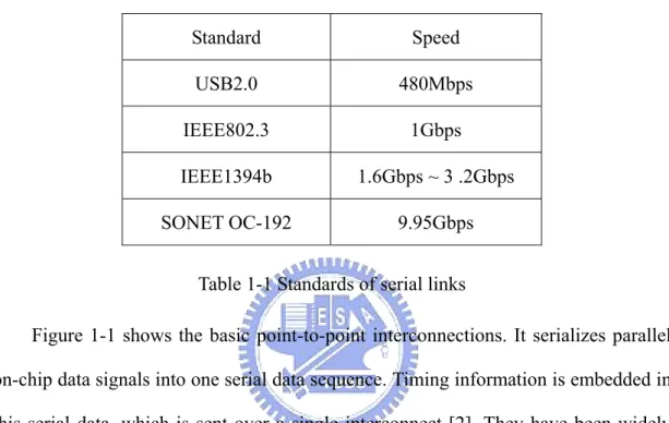
speed. Fortunately, CMOS technology has more improvement over other technologies due to the rapid size scaling. The architecture of most high performance communication switches is inherently based on point-to-point interconnections [1]. Therefore we can use both advantage to overcome this challenge. The industry standards of common and popular serial link are listed in Table 1-1.
Standard Speed USB2.0 480Mbps IEEE802.3 1Gbps
IEEE1394b 1.6Gbps ~ 3 .2Gbps
SONET OC-192 9.95Gbps
Table 1-1 Standards of serial links
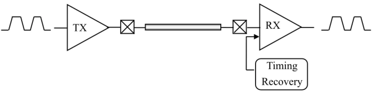
Figure 1-1 shows the basic point-to-point interconnections. It serializes parallel on-chip data signals into one serial data sequence. Timing information is embedded in this serial data, which is sent over a single interconnect [2]. They have been widely used in short-distance applications such as processor-to-memory interfaces, multiprocessor interconnections, communication with graphical display devices, backplane interconnections within a switch or a router, etc. In these links, the signaling techniques, non-return-to-zero pulse-amplitude modulations have been used and proven to be an effective scheme in communication through low-loss transmission chancel.
Fig. 1-1 Basic point-to-point interconnection
1.2 Thesis Organization
This thesis comprises five chapters. This chapter illustrates the research motivation.
Chapter 2 describes the background study. We will introduce transceiver and their basic concepts. In addition, we compare three different types of CDR and discuss design considerations in this chapter.
In Chapter 3, we describe the CDR in a receiver. A 2.5Gbps CDR is proposed in all digital approaches. The bandwidth of the confidence counter for an frequency offset of 5000ppm is discussed.
In Chapter 4, we describe remained blocks of the transceiver. First we chose shifted-register-type serializer and deserializer. Second, we chose a modified LVDS driver to meet our design target. Third, we implement the receiver-front end in all digital approach.
Finally, Chapter 5 concludes this thesis and discusses the future development.
TX RX
Timing Recovery
Chapter 2
Background Study
2.1 Basic Serial Link
In a point to point serial link system, we can classify a mesochronous system and
plesiochronous system by how the sampling clocks are derived. In a mesochronous
system the phase relationship between the transmitter and receiver is unknown [3]. However, in a plesiochronous system, the transmitter and receiver have similar but slightly different clock frequencies. Usually, the clock recovery mechanism in a
mesochronous systems is simpler than that in a plesiochronous system because only
phase locking is necessary.
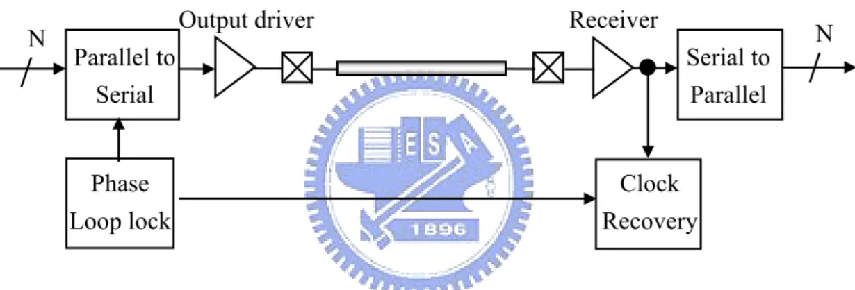
A generalized model of a serial link is illustrated in Figure 2-1. It consists of a transmitter, a channel and a receiver. The transmitter side serializes the parallel data
and delivers the synchronized data into the channel. The receiver side receives the serial data and recovers its timing. Finally, the serial data becomes parallel one.
In practice, the transmitter drives a HIGH or LOW analog voltage onto the channel for a particular output-voltage swing as determined by the system specification. The Receiver on the other end of the channel recovers the signal to the original digital information. To recover the bits from the signal, the analog waveform is amplified and sampled. Then an additional circuit, the timing-recovery circuit, properly places the sampling strobe.
Fig. 2-1 A generalized model of a serial link
2.1.1 Introduction of Jitter
Jitter also called Timing jitter is the time-domain phase noise. It expresses the time difference between the expected transition of the signal and the actual transition. Jitter can be defined into two types. One is called deterministic jitter which is the predictable component of jitter. The other are called random jitter that is the remaining components of jitter. Random Jitter (RJ) is related to thermal, flicker and shot noise sources. Deterministic Jitter (DJ) is related to crosstalk, ISI, Duty-Cycle
Distortion (DCD). Word-synchronized distortion due to imperfections within a data
Serial to Parallel Receiver N N Phase Loop lock Clock Recovery Output driver Parallel to Serial
serializer and other bounded jitter sources. In a CDR system we usually concern two specifications which can show the effect of jitter.
2.1.2 Jitter Tolerance
Jitter tolerance defined as input jitter a receiver must tolerate without violating system BER specifications. We can test tolerance compliance by adding a peak-to-peak amplitude of sinusoidal jitters at various frequencies (with amplitude greater than the mask) to the data input and observing bit error rate. Figure 2-2 shows the jitter tolerance mask for OC-192 spec.
Fig. 2-2 Jitter tolerance mask.
2.1.3 Jitter Transfer
Jitter transfer is defined as the ratio of jitter on the output of a device to the jitter applied on the input of the device versus jitter frequency. Jitter transfer is important
because it can quantify the jitter accumulation performance of data retiming devices.
We can test jitter transfer by adding sine wave jitters at various frequencies and observing the resulting jitter at the CDR output. Figure 2-3 shows the jitter transfer for OC-192 spec.
Fig. 2-3 Jitter tolerance mask
2.1.4 Bit Error Rate
In data transmission, the Bit Error Rate (BER) is the percentage of bits that have errors relative to the total number of bits received in a transmission.
BER is a merit of figure for the link performance. It also presents the reliability of the link. Too high the BER may indicate that a slower data rate would actually prolong the overall transmission time for a given amount of transmitted data. As a
bits d transmitte of number bits erroneous of number BER= ÷
result, the BER is specified in many industrial specifications such as IEEE 802.x, Gigabit Ethernet, SONET, OC-48, OC-192…, and etc.
There are some contributors which make the BER increases. First, the influences of noise on the transmitted signal and the noise induced in the receiver. Second the ISI will also cause errors because of the characteristics of circuit operations.
2.2 Techniques of Timing Recovery
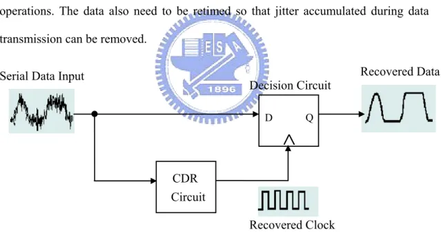
Figure 2-4 shows the functionality of CDR, A clock recovery circuit in a receiver is used to reconstruct the clock. Because the data received in a receiver are asynchronous and noisy. Thus, it requires that a clock be extracted for synchronous operations. The data also need to be retimed so that jitter accumulated during data transmission can be removed.
Fig. 2-4 Functionality of clock and data recovery
2.2.1 PLL Based Clock and Data Recovery Circuit
The basic architecture of a PLL-based CDR is shown in Figure 2-5. It’s a feedback system that operates like a traditional PLL. Random data, instead of a reference clock, is used as an input signal. A retimer is added on to the system can
D Q
CDR Circuit Serial Data Input
Decision Circuit
Recovered Clock
reconstruct the input data. The output of PLL_based CDR is directly aligned to the incoming data. The clock phase position located at the center of input data eye.
Fig. 2-5 PLL-based CDR
A PLL-based CDR consists a Phase Frequency Detector (PFD), a charge pump (CP), a Low-Pass Filter (LP filter), a Voltage-Controlled Oscillator (VCO), and a retimer or a decision circuit.
The Phase Detector (PD) detects the phase difference between the sampling clock phase and input data. It must have the capability to tolerate the missing pulse. There are two types of PD, Hogge’s PD (linear type) and Alexander PD (bang-bang type) [4] [5].
Figure 2-6 shows the basic Hogge’s PD and its transfer function. It contains 2 DFFs and 2 XOR gates. The output of Hogge’s PD will shows the phase difference amount and polarity.
Retimer PFD & CP LPF VCO Data In Recover Clock Data Out
Fig. 2-6 The basic Hogge’s PD
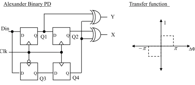
Figure 2-7 shows the basic Alexander PD and its transfer function. It contains 4 DFFs and 2 XOR gates. The result of phase detection only tells the polarity, whether leading or lagging. The amount of phase difference is not detected. Thus, the jitter is constantly produced at every phase detection.
Fig. 2-7 The basic Alexander PD
The phase difference is converted into VCO control voltage. The high frequency noise in this control voltage is filtered out by the loop filter. The loop adjusts the frequency of the voltage-controlled oscillator by the control voltage (Vctrl) until the phase is exactly the same as the input data. When the phase between the data input and VCO output are match, the VCO output will provide the sampling phase to the
D Q D Q Y X Din Clk Q1 Q2 π π − l ΔΦ Hogge’s Binary PD
π − π ΔΦ l D Q D Q D Q Q D Din Clk Q3 Q1 Q2 Q4 Y X
Alexander Binary PD Transfer function
decision circuit for retiming the input data.
For a feedback system, the stability is a major problem. The tracking bandwidth is limited by the stability of the feedback system. In general, the loop bandwidth of the PLL is usually set 1/20~1/40 of the reference clock. But this will limit the PLL track bandwidth and the ability to track the clock jitter.
Another similar architecture is the delay_locked loop type, It replaces the VCO block by a voltage control delay line (VCDL) A VCDL is composed of delay cells. The phase of the reference clock is tracked by controlling the different delay of the VCDL.
2.2.2 Oversampling Based Clock and Data Recovery
Circuit
The over-sampling block diagram is shown in Figure 2-8. The input data is sampled with the multiple phases generated by the clock generator in a single bit period. It requires at least 3 samples per bits. So, if the input frequency changes the sampling clock must be also changed.
Fig. 2-8 Oversampling-based CDR Multi-phase Data Receiver PLL/DLL Delay PhDet Filter Select Clk0-n Mux Data Output Data Recovery Ref_Clk Data Input
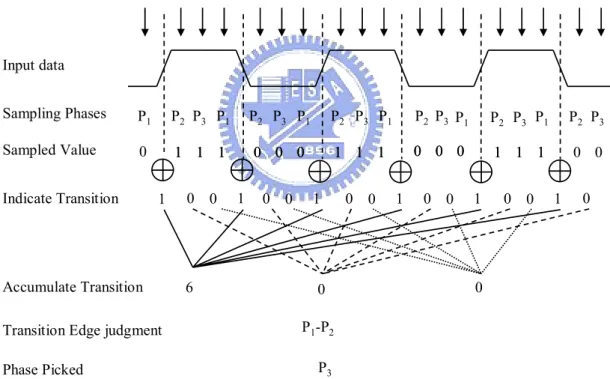
After the over-sampling, the transition in the data must be detected by using digital approach architecture. The algorithm employed in this work uses the transition position to determine the bit-window boundary and the optimum sampling point is picked. This method essentially employs a feed-forward loop. The high tracking rate is possible without the loop bandwidth problem.
For example, the data is sampled by 3 phases per bit time is shown in Figure 2-9. It decides the boundary with a portion of a sampled stream. First the neighboring data are XORed. Then the transitions are accumulated. The transition that has the highest accumulated count is the data transition edge. Then we can choice p2 as sampling phase [6]. P1 P2 P3 P1 P2 P3 P1 P2 P3 P1 P2 P3 P1 P2 P3 P1 P2 P3 Input data Sampling Phases Sampled Value 0 1 1 11 1 1 0 0 00 0 0 1 1 11 1 1 0 0 00 0 0 1 1 11 1 1 0 0 Indicate Transition 1 0 0 1 0 0 1 0 0 1 0 0 1 0 0 1 0 Accumulate Transition 6 0 0
Transition Edge judgment P1-P2
Phase Picked P3
Fig. 2-9 Time diagram of the oversampling
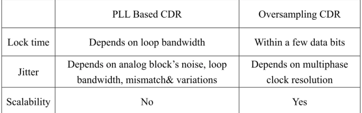
2.2.3 Comparisons
Table 2-1 shows the difference between PLL based CDR and oversampling based CDR. The PLL type can reach the exact phase. So, the output jitter is small, but the tracking ability is limited by loop bandwidth. In the oversampling type the output
jitter is determined by the resolution of neighboring clock phases. The advantages of oversampling type are simpler implement and reject the very high frequency jitter, up to the lesser of clock rate. Because of using the oversampling method, the hardware overhead will increase.
PLL Based CDR Oversampling CDR
Lock time Depends on loop bandwidth Within a few data bits
Jitter Depends on analog block’s noise, loop
bandwidth, mismatch& variations
Depends on multiphase clock resolution
Scalability No Yes
Table 2-1 Comparison of different typed CDR
2.3 Techniques of serializer
Serializer combines many low speed parallel random data into a high-speed stream of serial data. This technique reduces the buses for interconnections effectively Thus, it alleviates electrical and magnetic interference.
For example, most transmitters incorporate a 16-to-1 serializer. It allows 16 inputs to be much slower than the output. Hence, it simplifies the design of the package. This chapter describes the design of the all digitized CMOS data serializer. That is capable of running at a 2.5Gbps data rate, which can be adopted in optical transmitters.
2.3.1 Tree-Type Serializer
Figure 2-10 shows the data serializer with tree-type architecture. That is based on a set of 2:1 multiplexer circuits and uses a binary tree structure. To convert 16 parallel
control clock is half clock rate of which is used in next stage. Conventional 2:1 serializer is trigger during the every clock transitions. The latch in the final stage as a retimer. Hence, the jitter caused by previous stages cannot be accumulated. Therefore, the clean control clock in tree-type Serializer is very important. But, it’s difficult to produce the global clock for high speed operation.
The data serializer can achieve high-speed operation. Because the RC load of every multiplexer is not large [7]. The power consumption is lower due to the small number of high-speed-operated devices.
Fig. 2-10 Tree-type serializer architecture
2.3.2 Single-Stage Type Serializer
Time-division parallel-to-serial data conversion is achieved by gating each transmission path sequentially. Each branch acts as AND gate. The control signal of every transmitter gate is causing by phase of PLL [8]. The data serializer with single-stage type architecture is shown in Figure.2-11. Each data bit is transmitted at a time slot defined by the overlapping of the two controlled phases ie. Ck0 and Ck5. Figure 3.3 shows the single-stage type serializer timing diagram.
2:1 mux 2:1 mux 2:1 mux 2:1 mux 2:1 mux 2:1 mux 2:1 mux F/16 F/8 F/4 F/2 F 2:1 mux D0 D1 D1 D1
………...
OutFig. 2-11 Single-stage type serializer architecture
The maximum operating speed of this type is limited by large output parasitic capacitance. It is generated by a larger number of parallelisms and cannot increase transistor size to overcome this problem. Because increasing size also increasing plastic capacitance. Hence, this data serializer is commonly applied to the systems below 4Gbps.
Fig. 2-12 Timing diagram of Single-stage type serializer
…. ….
outa outb Ck0 Ck5 d0 Ck0 Ck5 nd0 Ck7 Ck4 d7 nd7 Ck4 Ck7Chapter 3
Clock and Data Recovery
3.1 CDR Tracking Method
In Chapter 2, we have described various architecture of CDR proposed in recent years. The CDR is usually used to solve phase problem in many application. It is essential to synchronize between data and clock to decrease BER.
Here we will introduce our CDR tracking method. Our CDR uses the phase shifting method to track the optimum phase. The phase change algorism is in linear search because it is easy to implement. We use clock rising edge as data sampling edge and the falling edge to deicide the bit boundary.
A tracking process is shown in Figure 3-1. The first sampling edge is rising edge. The second sampling edge is falling edge. The third sampling edge is rising edge of next period. The initial sampled sequence is “001”.
We know that the direction of phase shifting is decided by the output of the PD. The PD tells whether clock’s leading or laging the data. So the sampling phase will shift right or left until the phase is locked.
In Figure 3-1, the initial sampling phases are P1, the optimum sampling phases are between P2 and P3. After three times of changing sampling phases, the optimum sampling phase between “P2 and P3” is tracked.
Rule 1 Select the left phase as the sampling phase if the PD output lag=1 lead=0 hold=0 ”. Rule 2 Select the right phase as the sampling phase if the PD output lag=0 lead=1 hold=0”. Rule 3 The optimum sampling phase is found if phase change back and forth.
Fig. 3-1 Example of a tracking process
0 0 1 0 0 1 0 0 1 0 1 1 P1 P2 P3 P4 (b) (c) (a) (d)
3.2 CDR Architecture
First of all, we need a clock generator to generate a 4-phase clock as the clock source. Alexander phase detectors will get the relationships between the input data and the sampling phases. Then, the leading/lagging/holding signal will be delivered to the confidence counter. The counter in this system works as the low pass filter. If the counter has any overflows, the lead_ov/lag_ov signal will change the phase control finite state to generate appropriate phase control signals. Phase interpolator will select two neighboring phases and interpolate them to generate new phase position. The new phase is near the optimum phase. we can recover the data directly by using the optimum sampling phase. The CDR is designed to spread spectrum clocking (SSC). So we can handle 5000ppm frequency offset between input data and internal clock. The architecture of our CDR circuit is shown in Figure 3-2.
Fig. 3-2 Architecture of the proposed CDR
2 4 APD CC FSM PI 2.5Gbps Recovered Data Lead Hold Lag Lead_ov Lag_ov 2.5G clk 4
•APD: Alexander phase detector •CC :Confidence counter •FSM : Phase control •PI : Phase interpolator 2.5Gbps
3.3 Building Blocks
Each block in Figure 3-2 will be described respectively in the below paragraphs.
3.3.1 Multi-phases Phase Locked Loop
An 8-phase PLL [9] is applied as a frequency source for the purpose of
multi-phase sampling. The PLL is a ring oscillator operates at frequency of 1.25GHz. We use xor gate to generate 4-phase 2.5GHz clock.
3.3.2 Alexander Phase Detector (APD)
Chapter 2, we compare different PDs. The architecture of APD is shown in Figure 3-4. The phase detector in the CDR extracts the relationships between the input data transitions and the edges of sampling phases. Whether a data transition is present and whether the clock lead or lag the data [17]. Figure 3-3 illustrates the APD principle. It also knows as the lead-lag detection method. The XORs of three data samples,
S
1 S
⊕
2
andS
2
⊕
S
3
provides the lead or lag information. If lead=1、 lag =0 then the clock falling edge is lead data. If lead=0、lag =1 then the clock falling edge is lag data. If hold=1, then no data transition is present. So Alexander phase detector is a good approach in this field.Clk lead Clk lag A B C Din Clk Time A B C Din Clk Time 0 0 0 0 0 1 1 1 1 0 1 1 0 1 0 1 0 0 0 0 1 1 0 0 1 1 0 hold Lag Lead A B C 0 0 0 0 0 1 1 1 1 0 1 1 0 1 0 1 0 0 0 0 1 1 0 0 1 1 0 hold Lag Lead A B C
Fig. 3-4 Architecture of APD
3.3.3 Confidence Counter
Because the data is easily affected by noise. It will tell erroneous information of clock’s leading or lagging. So we use a confidence counter here to play a role of digital low pass filter. It prevents the influences on the system performance due to the noise effects. Such as signal distortions or ISI [10]. Traditionally, the confidence counter has two types. One type is the continuation type. Only when there are leads or lags continually N times, the confidence counter is activated. The other type is the accumulation type. When the numbers of lead or lag accumulates N times, the confidence counter is activated.
The state diagram is shown in Figure 3-5. Here we use an accumulation type counter with one-hot-state design. It has lower the glitches effect and is suitable for
D Q D Q D Q D Q Clk B C lag lead hold Q Qb D Db ck ckb A
high speed operation.
The confidence counter works in a token transfer manner. When token transfer out of range, the token will start at middle of the register’s chain and send the overflow message. Now we have to change the sampling phases. In other words, to design such a high speed counter must be more carefully. The circuit is shown in Figure 3-6.
Fig. 3-5 State diagram of the confidence counter.
Fig. 3-6 Architecture of the confidence counter.
gnd gnd
…
…
Reset CLK Left right Hold_FSM Hold Right Left Lead_FSM X6 X7 X5 X8 X9 X4 X3 L R L R X11 X2 X1 H X12 Lag_FSM3.3.4 Phase Control (Finite State Machine)
A finite state machine is designed as a control logic block. It tells the system which state is present state and which output will be considered as the recovered clock and the recovered data. When the phase control receives lead_ov or lag_ov signal from the confidence counter. It controls the phase interpolator to adjust clock with a phase resolution. The state diagram and the phase change behavior are shown in Figure 3-7.
Fig. 3-7 (a) State diagram (b) Phase behavior 1000 1100 1110 1110 1100 1000 0000 0011 0111 0001 1111 1111 0000 0001 0011 0111 P0&P1 interpolator (a) P0 P1 … P2 … B A Course control Course control fine control fine control (b)
The phase control includes two parts. One is fine tune and the other is coarse tune. The coarse tune determines two neighboring phase which difference is 100p.The fine tune determines the optimum phase between the neighboring phase. So the fine tune must works after coarse tune. The behavior of the phase change is linear change and the control word change like thermal code.
The architecture of the phase control is shown in Figure 3-8. The fine tune is shift register type. The coarse tune is a combinational circuit generated by Karnaugh map.
Fig. 3-8 The architecture of phase control (a) Fine tune (b) Coarse tune (b) D3 Coarse tune: C1 C1b C0 C0b Ph0 … C0 C1 Ph3 D0~3 D0~3b Ph1 Ph2 … C1b C0b clk Coarse2_control Coarse1_control Coarse1_control: Coarse2_control: D0 Lead-FSM Lag-FSM Lead Lag Hold D0b Lead-FSM Lag-FSM Lead Lag Hold D3b D3 Coarse tune: C1 C1b C0 C0b Ph0 … C0 C1 Ph3 D0~3 D0~3b Ph1 Ph2 … C1b C0b clk Coarse2_control Coarse1_control Coarse1_control: Coarse2_control: D0 Lead-FSM Lag-FSM Lead Lag Hold D0b Lead-FSM Lag-FSM Lead Lag Hold D3b D0 D1 D2 D3 clk (a) Lead-FSM Lag-FSM Hold-FSM
3.3.5 Phase Interpolator
The utility of the interpolator is to interpolate one signal between two phases. Figure 3-9 shows the architecture of phase interpolator. The interpolator composed of two parallel sets which are composed of tri-state inverters and their output are short together. We can generate the phase by adjusting the relative drive strengths of the two sides. Because the basic cell of interpolator is tri-state inverter. Hence, the number of turn-on inverters can be controlled digitally.
The architecture of phase interpolator is shown in Figure 3-10. The coarse tune control the phases Ph0~Ph3 which have a difference 100ps between each phase. The phase can be rotated by change coarse tune control bits. The behavior of fine tune control varies the contribution of two input edges. This method generates the new phase. The output and linearity of phase interpolator is shown in Figure 3-10.
Fig. 3-9. The architecture of phase interpolator 4bit Ctrl Ph2 Ph1 Ph3 Out 100p Delay Ph0 Ph0 Ph1 Out
(a) step# 0 1 2 3 4 % of phas e in te rval 0 20 40 60 80 100 ideal simulated (b)
Fig. 3-10. The output and linearity of phase interpolator
3.4 The Analysis of Confidence Counter
Size
However, how we know the size of counter should be? In [13][14] we can observe increase counter size will decrease the output jitter. It tells us large counter size indicate narrow loop bandwidth (if the phase resolution is fixed) can filter high frequency noise. But counter size cannot be arbitrarily increased, because there are some frequency offset between the embedded clock of incoming data and local clock.
The narrow loop bandwidth indicates slow tracking ability.
Therefore, we understand the counter size is relative to phase change resolution. For our target to work with spread spectrum clocking. Our design can trace the frequency offset until 5000ppm. From (3-1) we can understand the relationship between counter sizes, phase resolution and frequency. dis the transition density
and fΔ is frequency it has units of parts-per-million(ppm).L is the phase resolution steps. f L J Q N d rms Δ = ⎥ ⎥ ⎦ ⎤ ⎢ ⎢ ⎣ ⎡ ⎟⎟ ⎠ ⎞ ⎜⎜ ⎝ ⎛ Δ −2 φ 1 (3-1)
In Figure 3-11, we assume that the distribution of jitter is normal distribution. When frequency difference between data and clock, the sampling phase has to be to the left(right) of the center position in order to increase lead(lag)probability to track
the input data. The
⎥ ⎥ ⎦ ⎤ ⎢ ⎢ ⎣ ⎡ ⎟⎟ ⎠ ⎞ ⎜⎜ ⎝ ⎛ Δ − rms J Q φ 2
1 is the probability which getting a lead transition
more than lag transition (the leading probability subtracting the leading probability).
,
Fig. 3-11 Normal distribution of jitter. 400ps
φ
Δ
Figure 3-18 shows the jitter tolerance versus counter size. Because input data is
Pseudo Random Bit Sequence (PRBS). So the transition density is 0.5. From (3-1) we
also know when a certain frequency offset is desired. The maximum phase lag/lead in the CDR design can also be determined. Therefore, there is a direct tradeoff between low jitter on the recovered clock and the ability of the CDR to track large input frequency offsets. This phase error phenomenon is similar to the steady-state phase error observed in a first-order PLL.
counter 0 2 4 6 8 10 F re que ncy O ffse t(ppm ) 0 5000 10000 15000 20000 25000 30000
Fig. 3-12 The jitter tolerance versus the counter size
In the discrete-valued case, Markov chain is a sequence of random
variablesX1,X2,X ,..,3 Xnwith Markov property given the present state. The next and
past states are independent. Formally,
)
Pr(
)
,
,...,
Pr(
X
n+1=
x
X
n=
x
nX
1=
x
1X
0=
x
0=
X
n+1=
x
X
n=
x
n . (3-2)The possible values ofX form a countable set S called the state space of the i
chain. Markov chains are often described by a directed graph in Figure 3-13. In Figure 3-13 the edges are labeled by the probabilities of going from one state to the other states. If the chain is currently in state “Si”, then it moves to state “Sj” at the next step
with a probability denoted byP . This probability does not depend upon which states ij the chain was in, before the current state. The probabilitiesP are called transition ij probabilities. The process can remain in the state it is in. This occurs with probabilityP . ii s2 s1 P12 P21 P22 P11
Fig. 3-13 The state-transition diagram of Markov chain
From (3-3) we can understand the definition of P ij
)
Pr(X1 jX0 i
Pij = = = (3-3)
Define probability of going from state “ i ” to state “ j ” in n time steps as
)
Pr(X1 j X0 i
Pijn = = = . (3-4)
The n-step transition satisfies the Chapman-Kolmogorov equation, that for any 0<k<n
k rj(n k) ir S r n ij P P P − ∈Σ = . (3-5)
As mention before, the confidence counter is a digital filter. So we want to calculate the bandwidth of the counter, unlike the traditional analog filter which can be calculated by RC. In discrete time domain, we use Markov chain theory and expected value to calculate the bandwidth. First we use the first passage time of Markov chain theory. Figure 3-14 shows the Markov chain of the confidence counter.
s7 s6 s8 s9 s5 s4 s3 s0 s12 P67 P78 P56 P45 P34 P00 P89 P98 P87 P76 P65 P54 P43 •• •• P12 12
Fig. 3-14 The Markov chain of confidence counter
Using first passage time, we can modify (3-5)
) 1 ( ) (
∑
≠ −⋅
=
j k n kj ik n ijP
P
P
Fori=4 ,j=8mustn=4,6,8… (3-6)Now we use (3-10) to calculate the combinations of n
ij
P for different n
(3-7)
Second, we use the expected value of conditional probability to calculate the loop bandwidth of digital filter.
⎥
⎥
⎥
⎥
⎥
⎥
⎥
⎥
⎥
⎥
⎥
⎦
⎤
⎢
⎢
⎢
⎢
⎢
⎢
⎢
⎢
⎢
⎢
⎢
⎣
⎡
0
14
0
14
0
6
0
1
0
0
0
0
5
0
9
0
5
0
1
0
0
0
0
0
0
5
0
4
0
1
0
0
0
0
0
0
2
0
3
0
1
0
0
0
0
0
0
0
0
2
0
1
0
0
0
0
0
0
0
0
1
0
1
0
0
0
0
0
0
0
0
0
0
1
0
0
0
0
0
0
0
0
0
0
1
0
0
0
0
0
0
0
0
0
0
0
n P11,12 n P10,12 n P9,12 n P8,12 n P7,12 n P6,12 n P5,12 n P4,12 n P3,12 n P2,12 n P1,12 n P0,12 N=1 N=2 N=3 N=4 N=5 N=6 N=8 N=7(3-8)
From the (3-11), we can observe the bandwidth of filter is related to lead (lag) probability which caused by the sample point of data. Figure 3-15 shows the bandwidth versus lead probability. When the probability of lead is the same as lag, the bandwidth is ≈34.7MHZ. transition Pro. 0.5 0.6 0.7 0.8 0.9 1.0 ban dwi d th (M h z ) 20 40 60 80 100 120 140 160 180 200 transition Pro. 0.5 0.6 0.7 0.8 0.9 1.0 steps 10 20 30 40 50 60 70 80
Fig. 3-15 The bandwidth versus lead probability
) 1 ( ... ) 1 ( 110 ) 1 ( 27 ) 1 ( 6 ) 1 ( 1 ... ) 1 ( 1638 16 ) 1 ( 429 14 ) 1 ( 110 12 ) 1 ( 27 10 ) 1 ( 6 8 ) 1 ( 1 6 )] ( [ 0 4 3 7 2 8 1 7 0 6 * 5 11 * 4 10 * 3 9 * 2 8 * 1 7 * 0 6 *
∑
∞ = + − ℘ = + − × × + − × × + − × × + − × × = + − × × × × + − × × × × + − × × × × + − × × × × + − × × × × + − × × × × = k k k kp p p p p p p p p p P p p p T p p p T p p p T p p p T p p p T p p p T t x E3.5 Experiments
3.5.1 System Behavior Simulation
Owning to the CDR system simulation with SPICE takes a lot of time. We use MATLAB SIMULINK to analyze the system behavior and verify the lock function. Functional verification of the CDR is performed effectively at the first design step, which improves turn around time of CDR design. Figure 3-16 shows the behavior model of the CDR. Figure 3-17 shows the functional verification of the CDR. We can observe when the CDR in locking state, the control will jump between two control bits. Figure 3-18 shows the jitter cause by tracking frequency offset; we can observe output jitter about 2LSB.
Fig. 3-17 Control bits of CDR
Fig. 3-18 Output jitter of tracking frequency offset
Figure 3-19 shows the clock output jitter with different data input jitter. The output jitter of the worse case (input jitter=0.6UI) is 2LB. We can claim that our proposed can generate recovery clock cleanly at worse case.
.
160p
240p
output input
Fig. 3-19 The output jitter versus input jitter
The simulation result of the CDR circuit is given in Figure 3-19. We can see our input is PRBS. The APD receives the data and tells the system the relationship between data and clock by signals lead, lag and hold. When the confidence counter accumulates enough leads or lags. It will sends lead_ov or lag_ov to phase control. Hence, when lead_ov and lag_ov appear reciprocally. we can say the data is locked by clock, the output jitter of recovered clock is the minimum phase resolution. Figure 3-20 shows the eye diagram of the post-layout simulation.
CDR_in CDR_clk lead hold lag lead_ov lag_ov c0 c1 d0 d1 d2 d3 APD Confidence counter FSM
Fig. 3-20 Simulation of the CDR function verification.
Fig. 3-21 Eye diagram of the post-layout simulation 32p
3.6 Summary
An all digitized 2.5Gbps clock and data recovery circuit with the 0.18um CMOS technology. The feature of this CDR is tracking frequency offset of 5000ppm.it is implemented with all digitized circuits. The all digital approach will lower the design complexity and adaptive to the improvement of technology. The area and the power
Chapter 4
2.5Gb/s Transceiver with Digitized
Architecture
4.1 Introduction of transceiver
Figure 4-1 shows the overall transceiver architecture. Our transceiver is proposed with digitized architecture besides PLL which is mixed mode circuit. In the transmitter, it consists of a multi-phase PLL for data transmission, a serializer and an LVDS output driver. The serializer converses parallel data to serial, its clock is provided by a PLL. The role of the output driver is to drive serial data to physical channel and provide good driving capability to avoid ISI.
the physical channel and amplify the data swing. The CDR synchronizes the input data and the system clock, finally deserializer converses the serial data to Parallel which can be handled by decoder.
Fig. 4-1 The architecture of transceiver
4.2 Shift-Register Type Serializer
Figure 4-2 shows the architecture of the data serializer with shift-register type. Figure 4-3 shows timing diagram. It divides into two parts, one is parallel load, the other is serial shift. In low operation speed part use static DFF. In high operation speed part use True Single Phase Clocking (TSPC), In order to reduce power consumption.
Compare with other types, our design is 10-1 serializer. Hence, we can not choose tree-type architecture. Besides, if we choose single-stage type serializer architecture, we need 10 precise phases clock. The limitation of shift-register type is the maximum operate frequency of DFF and it has the advantage of flexible number of parallelism. 10bits 10-1 Serializer 8 phase 1.25GHZ 10 bits 100M CDR 2.5Gbps PRBS 8 phase 1-10 Deserializr Driver Receiver
Figure 4-4 shows the simulated eye diagrams of the data serializer, Figure 4-5 shows the timing simulation of serializer. From this simulation information, we can preliminarily assure the circuit function is correct.
Out 1 0 Ck4 D Q D Q D Q D Q D Q
1
D Q D0 D6 D8 D Q D Q D Q D D Q D Q D Q D1 D7 D9 Ck1b Ck1 Ck2 Ck3 0 0 Serial shift Parallel load Out1 Out0……
……
D Q……
……
Out 1 0 Ck4 D Q D Q D Q D Q D Q1
D Q D0 D6 D8 D Q D Q D Q D D Q D Q D Q D1 D7 D9 Ck1b Ck1 Ck2 Ck3 0 0 Serial shift Parallel load Out1 Out0……
……
D Q……
……
Fig. 4-2 Architecture of serializer
D1 D0 D2 D3 D4 D5 D6 D7 D8 D9 D8 D9 D1 D0 D2 D3 D7 D6 Ck1 Ck2 Ck3 Out Out1 Out0 D9 D8 D7 D6 D5 D4 D3 D2 D1 D0 D1 D0 D2 D3 D4 D5 D6 D7 D8 D9 D8 D9 D1 D0 D2 D3 D7 D6 Ck1 Ck2 Ck3 Out Out1 Out0 D9 D8 D7 D6 D5 D4 D3 D2 D1 D0
Fig. 4-4 Eye diagrams of the serializer 1 1 0 0 1 0 1 1 0 1 D0 D1 D2 D3 D4 D5 D6 D7 D8 D9 ck3 ck2 ck1 Ser-out LFSR 1 1 0 0 1 0 1 1 0 1
Fig. 4-5 Timing simulation of serializer
4.3 LVDS Driver
This section roughly describes the output driver design in[1], this driver part has been verified. Figure 4-6(a) shows the traditional Low-Voltage Differential Signaling (LVDS) driver, it includes two current sources to minimize the current change hence reduce noise[11] [12]. But these two current sources will create a large voltage drop
Figure 4-6(b) is proposed LVDS driver. It removes current sources, the whole driver architecture looks like the two inverters connected back to back, it makes the control and layout easier. It also reduces the sizes of the cell greatly, with same output voltage swing.
Fig. 4-6 (a) Traditional (b) Our proposed LVDS driver
4.4 Generation of random data
In order to test transmitter independently, we put a data generator in transmitter, but it is difficult to generate completely random binary data because for the randomness to manifest itself. For this reason, it is common to employ a PRBS. It is 'pseudo' because it is deterministic and after N elements it starts to repeat itself, unlike real random sequence.
As shown in Figure 4-7, there are sixteen DFF as the shift registers and an XOR gate to send the result to the input of the first DFF. Figure 4-8 shows HSPICE simulation results. Vip Vin Vin Vip Vip Vin Vin Vip
(a)
(b)
A 216− data pattern can be generated with sixteen registers and an XOR 1 circuit. The characteristic of the PRBS architecture is that it can generate all possible combination patterns except all zero vectors. The probability of transitions from 0 to 1 and 1 to 0 are the same as 50%. It is a simple and regular structure. This technique can be extended to an m-bit system so as to produce a sequence of length 2m 1
−
Fig. 4-7 Linear feedback shift registers
D0 D1 D2 D3 D4 D5 D6 D7 D8 D9 clk D D QQ
…
D0 D1 D6 D7 D8 D9 D1 D1 D7 Clk Q Q D D DD QQ QQ Q Q Q Q Q Q Q Q D D D D D D D D D D…
D15 D74.5 Receiver front-end
When the differential data imports to the chip, they are distorted. Because of the inductance and capacitance resonance caused by boning wire and pad. Hence, receiver front-end play an important role to sense received signals, either from the system clocks or the input data stream which usually has large jitter, small amplitude swing. Therefore input sensitivity, symmetry and bandwidth are major concerns.
The receiver can generate output of ‘1’ or ‘0’ by detecting the difference of input
differential voltage
v
d (vin+ −vin−). Ifv
d is positive, the output of receiver frond-end will be Vdd. Ifv
d is negative, the output of receiver frond-end will be gnd.Figure 4-9 shows the architecture of receiver front-end. Our proposed architecture is all digitized. it operates in fully differential, and amplify the swing of the input signal stage by stage. We use two inverters which connect input to output by each other to make hysteresis. It makes the signal transfer with symmetry and reduce the effect of noise. The inverter connects with transmission gate here has two advantages. One is inverter (input and output connect together)can make input
common-mode at 2 1
vdd. We don’t need common-mode feed back circuit. The other is
inductive peaking, the transmission gate act as resister. Therefore, we reduce the gain but extend the bandwidth of the inverter. In order to reach large swing, we need more stages.
Fig. 4-9 Architecture of receiver front-end
Figure 4-10(a) shows the output for each point. We can see at the node B the swing is enough. From A to D the jitter is decrease. Figure 4-13(b) shows the common-mode variation for each point. The variation from A to D is decrease, so our proposed design is not sensitive to common-mode variation.
A B C D Output (a) A B C D Output A B C D Output (b)
Fig. 4-10 (a) Output swing (b) Common-mode variation
In
Inb
4.6 Deserializer
The deserilaizer is necessary, because the decoder which work as parallel. The deserializer puts a serial high-speed stream into many low speed random data. Therefore, the deserializer works like serializer just puts the serial data to parallel data.
Figure 4-11 shows the architecture of deserializer. The ck3 as parallel load control, its frequency is 250 MHz. The ck1 is switch control which separates odd number and even from the data stream. Figure 4-12 shows the timing diagram of the deserializer. The output data rate is 250Mb/ps. The eye diagram of deserializer is shown in Figure 4-13. Q Ck1 D Q D Q Ck1b Ck3 D Q D Q D Q D Q D Q D Q D Q D Q D Q D Q D8 D6 D0 D9 D7 D1 Data A B C
……
……
D……
……
Q Ck1 D Q D Q Ck1b Ck3 D Q D Q D Q D Q D Q D Q D Q D Q D Q D Q D8 D6 D0 D9 D7 D1 Data A B C……
……
D……
……
Fig. 4-11 Architecture of deserializer
( (2.5G)ClK CK3 D0 D1 D2 D3 D4 D5 D6 D7 D8 D9 D0 CK1 D9 D1 D3 D5 D7 D9 D8 D0 D2 D4 D6 D8 D0 D2 D4 D6 D8 Data A B C ( (2.5G)ClK CK3 D0 D1 D2 D3 D4 D5 D6 D7 D8 D9 D0 CK1 D9 D1 D3 D5 D7 D9 D8 D0 D2 D4 D6 D8 D0 D2 D4 D6 D8 Data A B C
Fig. 4-13 Eye diagram of deserializer
4.7 Tape Out
The proposed 2.5Gb/s transceiver is implemented by National Chip Implement Center (CIC) with T18-95D. The chip area is 1360µm*1360µmm as shown in Figure 4-14. The timing diagram of the transmitter is shown in Figure 4-15. The chip will be implemented and send back in October 2006.
25p
Fig. 4-15 Eye diagram of transmitter
In order to verify the function of the transceiver in detail, we use two methods to verify function bypass different way. One is LFSR mode, the data generated by LFSR, then through channel, finally we observe the output of CDR. The functional verification is shown in Figure 4-16, The other is loop-back mode, we use BER as the data source. The receiver receives the data and through the CDR, finally we observe the output of the transmitter. The functional verification is shown in Figure 4-17.
LFSR data 1 0 1 1 0 1 0 1 0 1 TX_out cdr_out 1 0 1 1 0 1 0 1 0 1 10 1 1 0 1 0 1 0 1
RX_in cdr_out Deser_out 0 1 0 0 0 0 0 1 0 TX_out 0 1 0 0 0 0 0 1 0 0 1 0 0 0 0 0 1 0
Fig. 4-17 Functional verification of loop-back mode
4.7.1 Summary
In this chapter, we introduce the remained part of the transceiver. We implement circuit with digitized architecture besides PLL. Because digitized architecture without current source. Hence, our design can reduce power dissipation. The output data rate of the transceiver is 2.5Gb/s. The area and the power dissipation of the
transceiver_core are350µm*675µmm and 115mWatt. The post-layout simulation
Function 2.5Gbps Transceiver Technology 0.18um 1P6M
Chip size 1360*1360(um2) Core size 350*675(um2) Power Dissipation ~115mW Function PLL Size 305*315 (um2) Power Dissipation 30mW Function TX Size 356*143 (um2) Power Dissipation 27mW Jitter (pk-pk) ~25p @2.5Gbps Function RX Size 356*162 (um2) Power Dissipation 58mW CDR_jitter(pk-pk) 32ps @2.5Gbps Frequency_offset 5000ppm
Chapter 5
Conclusion
5.1 Conclusion
This thesis describes the transceiver with digitized architecture in 0.18um 1P6M CMOS process. The transceiver works at 2.5Gb/s data rate with low power consumption and small core_area. Our proposed circuits are suitable for the wire communication in the present on-board connection system.
Chapter 3 describes a 2.5G/s CDR circuit with digital approach to synchronize data and clock. In order to increase phase resolution we use phase interpolator. Finally, we use MATLAB to establish the model of CDR. By this way we can verify the behavior of our design. The output jitter of the CDR is 32ps.
output driver, the receiver front-end and the deserializer. The serializer samples the data at the stable-state and transfers the data into the 2.5Gb/s serial data. The serial data is transmitted as low voltage differential signal by the output driver. The receiver front-end uses digitized architecture instead of traditional analog one. It does’t use the commom-mode feedfack circuit. The receiver front-end can amplifer the signal swing and reduce the data jitter. The deserializer samples the recovered data at the stable-state and transfers the parallel data into the 250Mb/s. The output jitter of the transmitter is 25ps.
5.2 Future Work
Due to the digitized transmitter design, we separate the driver into several small drivers. But we doesn’t use other circuit to ensure that the signal swing fits LVDS specification. We can control the transistors by digitized circuit due to the advantage of these separated transistors. So, we can realize digital swing calibration circuit technique.
In the CDR design we use digitized phase interpolation circuit to increase phase resolution, but the phase resolution can’t be control precisely. Some control circuits can be added, to control output jitter well.
Bibliography
[1] F.A. Tobagi, “Fast packet switch architectures for broadband integrated services digital networks,” Proceedings of the IEEE, vol. 78, no. 1, pp. 133-167, Jan. 1990.
[2] S.H. Hall, G.W. Hall, et al. , “High-Speed Digital System Design— A handbook of
interconnect theory and design practices,” Wiley-Interscience Publication,2000.
[3]W.J. Dally and J.W. Poulton, “Digital Systems Engineering,” Cambridge University Press, 1998.
[4] B. Razavi, “Challenges in the design of high-speed clock and data recovery circuits,” IEEE Communications Magazine, pp. 94-101, Aug. 2002
[5] C. R. Hogge, “A self correcting clock recovery circuit.,” IEEE J. Lightwave
Technology, vol.3, pp.1312-1314, Dec.1985.
[6] Chih-Kong Ken Yang, Ramin Farjad-Rad and Mark A. Horowitz, “A 0.5-μm CMOS 4.0-Gbit/s Serial Link Transceiver with Data Recovery Using
Oversampling,” IEEE JSSC, vol. 33, pp. 713-722, May, 1998.
[7] Cao, J.; Green, M.; Momtaz, A.; Vakilian, K.; Chung, D.;” OC-192 transmitter and receiver in standard 0.18um CMOS,” IEEE J. Solid-state Circuits, Vol. 37, No.12, Dec, 2002
[8] C.K. Yang and M.A. Howitz, “A 0.8-um CMOS 2.5Gb/s Oversampling Receiver and Transmitter for Serial Links,” IEEE I. Solid-State Circuits, Vo131, No. 12, Dec. 1996.
[9] J.-C. Hsu, “A 1.25-GHz, 8-phase phase-locked loop with low gain and wide tuning range VCO,” M.S. Dissertation, Department of Electrical Engineering, National Central University, Taiwan, July 2003.
[10] Y.-T. Chuang, “all digital 2.5Gps deskew buffer,” M.S. Dissertation, Department of Electrical Control Engineering, National Chiao Tung University, Taiwan, July 2004.
[11]S. Chun, M. Swaminathan, L. D. Smith, et al., "Modeling of Simultaneous Switching Noise in High Speed Systems," IEEE Journal of Solid-Sate Circuits, vol. 24, pp. 132-142,May, 2001.
[12] N. Na, M. Swaminathan, J. Libous, et al., "Modeling and Simulation of Core Switching Noise on a Package and Board," presented at IEEE Electronic
Components and Technology Conference, 2001.
[13] M.-J. E. Lee, W. J. Dally, J. Poulton, T. Greer, J. Edmondson, R. Farjad-Rad, H.-T. Ng, R. Rathi, and R. Senthinathan, “A second-order semi-digital clock recovery circuit based on injection locking,” in IEEE Int. Solid-State Circuits Conf. Dig. Tech.
Papers, Feb. 2003, pp. 74–75.
[14] M.-J. E. Lee, W. J. Dally, T. Greer, H.-T. Ng, R. Farjad-Rad, J. Poulton, and R. Senthinathan, “Jitter transfer characteristics of delay-locked loops—Theories and design techniques,” IEEE J. Solid-State Circuits, vol. 38, pp. 614–621, Apr. 2003.
[15] H.Stark, J.Woods. “Probability and Random Processes with Applications to
Signal Processing,”Prentice-Hall Publication,2002.
[16] A.L. Garcia. “Probability and Random Processes For Electrical Engineering,” Addison-Wesley Publication,1994.
[17] Jri.lee, K.S.Kundert, B.Razavi, “Analysis and Modeling of Bang–Bang Clock and Data Recovery Circuit,” IEEE J. Solid-State Circuits, vol. 39, pp. 1571–1580, Sept. 2004.