Chapter 2
Experimental details
2.1 Instrumentation
---UHV variable-temperature STM system
All experiments were performed using a commercial ultra-high vacuum, variable-temperature scanning tunneling microscopy (UHV-VT STM, Omicron).
The apparatus (Fig. 2.1), which comprised of a UHV pumping system, a sample preparation chamber, an STM system, two well-collimated e-beam evaporators for in-situ deposition of high purity Pb and Ag, and a cryostat, cooled the sample to approximately 100K using liquid N2 or to 25K using liquid He.
2.2 Tip preparation
The STM tips used in this work were W tips. A piece of W wire (∅
0.3 mm) was used as a tunnel tip, which was prepared by electro-chemical etching in a saturated KOH solution using a DC power supply.
12
Preparation chamber
Pb evaporator STM system Ag evaporator
Fig.2.1: Ultra-high-vacuum variable temperature scanning tunneling microscope (UHV VT STM) system, Omicron.
2.3 Surface preparation
The experimental sample was an Si(111) wafer. The crystal plane orientation of the wafer was under 0.1°; the thickness was 0.3 mm, and the N-type doping level was of the order of 1017 cm-3. The Si(111) wafer was cut to 9 mm long and 1.5 mm wide, and dust was blown off the Si pieces by ultrasonic cleaning in acetone or methanol. The VT STM samples were outgassed overnight by direct heating with a typical current 0.5 A for at a temperature that was sufficiently low not to remove the native oxide (≈ 650°C), until the pressure reached below 2×10⁻¹⁰mbar. The sample was flashed to 1200°C by direct current heating at a controlled pressure that did not exceed ≈ 2×10⁻¹⁰ mbar. A sequence of short heating cycles was applied until the sample remained at 1200°C for less than 10 sec.
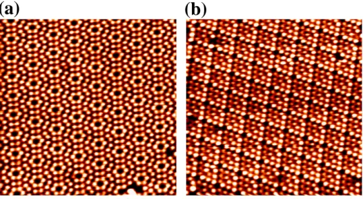
(a) Si(111)7×7
In the experiment, the Si(111)7×7 reconstruction surface was formed by heating to 1200°C several times over a total period of about 1 min., followed by sudden cooling to ~900°C and then slow cooling to room temperature at a rate of around 2°C per second. Figure 2.2 depicts the topography of the clean Si(111)7×7 surface.
14
(b) Pb phases on Si(111) surface
Various phases of Pb/Si(111) serve as a substrate. They include the bare Si(111)7×7 and the incommensurate phase of the Pb/Si(111) surface to elucidate the nucleation and growth behaviors of Pb quantum islands, or the phase transition of nearly one monolayer of Pb deposited on the 1×1 phase of Pb/Si(111), which was transformed into the 7× 3 phase at low temperature.
The incommensurate phase of the Pb/Si(111) surface was prepared by depositing one monolayer of Pb on the Si(111)7×7 at room temperature, followed by annealing at 480°C for one second.
The 1×1 phase of Pb/Si(111) was obtained by depositing approximately 0.6 monolayer (ML) of Pb onto the clean Si(111)7×7 surface at room temperature. After Pb had been deposited, the sample was annealed to about 480°C for a few seconds. A mixture of (1×1)-Pb and ML( 3 3)
3
1 × phases
was then observed.
(a) (b)
Fig. 2.2: Images showing Si(111)7×7 surface at the sample bias (a) +2V, and (b) -2V. Sizes of these images are 25nm×25nm.
16