應用於電源供應器前級 AC-DC 後級 DC-DC 錯相
脈寬調變控制器設計
Design of an AC-DC and DC-DC Interleaved PWM
Controller for Switching Power Supply
中文摘要:
本論文實驗一電源供應器之具前級交流轉直流與後級直流轉直流控制時脈錯相方
法。在傳統電源供應器當中,交流轉直流功率因數校正轉換器與後級直流轉直流轉
換器為個別獨立控制,因此無法降低 DC bus 上電流漣波。本論文將前級與後及控
制整合於一晶片中,前級功率因數控制電路利用單周期控制,使晶片之實現不需用
乘法器,即可達到高功率因數極低總諧波失真;後級直流轉直流控制器,採用電流
模式脈寬調變控制以達到良好的電壓調節率。藉此降低 DC bus 上之電流漣波並提
高效率。最後,本晶片採用 TSMC 0.25 UM CMOS HIGH VOLTAGE MIXED
SIGNAL BASED BCD 1P5M SALICIDE 2.5/5/60 V 製程實現。
Abstract :
In this paper, the AC-DC and DC-DC interleaved control for power supply is proposed. In
conventional power supplies, the front-stage AC-DC power-factor correction (PFC)
converter and the rear-stage DC-DC converter are controlled independently; therefore, the
current ripple on the DC-bus capacitor is uncontrolled and significant. One-cycle control is
used in the front-stage AC-DC PFC converter such that it achieves high power factor and
low current total harmonic distortion. The rear-stage DC-DC converter is controlled by
current-mode modulator to regulate the output voltage. Moreover, the power switches of
the front and the rear-stage converters are controlled with constant-frequency interleaved
control; consequently, the current ripple on the DC-bus capacitor can be reduced, which
leads to higher efficiency. The controller is implemented by the TSMC 0.25μm BCD
CMOS 2.5/5/60 V process.
Design of an AC-DC and DC-DC Interleaved PWM
Controller for Switching Power Supply
Tsung-Han Yu, Tsorng-Juu Liang, Senior Member, IEEE, Kai-Hui Chen, Ji-Shiuan Li, Ji-Shiang Lee
Department of Electrical Engineering/Advanced Optoelectronic Technology Center (AOTC)
/Green Energy Electronics Research Center (GREERC)
National Cheng Kung University, Tainan, Taiwan
Email:
[email protected]
Abstract—In this paper, the AC-DC and DC-DC interleaved
control for power supply is proposed. In conventional power supplies, the front-stage AC-DC power-factor correction (PFC) converter and the rear-stage DC-DC converter are controlled independently; therefore, the current ripple on the DC-bus capacitor is uncontrolled and significant. One-cycle control is used in the front-stage AC-DC PFC converter such that it achieves high power factor and low current total harmonic distortion. The rear-stage DC-DC converter is controlled by current-mode modulator to regulate the output voltage. Moreover, the power switches of the front and the rear-stage converters are controlled with constant-frequency interleaved control; consequently, the current ripple on the DC-bus capacitor can be reduced, which leads to higher efficiency. The controller is implemented by the TSMC 0.25μm BCD CMOS 2.5/5/60 V process.
I. INTRODUCTION
With the progress of the electronics industry, many consumer electronics products such as personal computers (PCs), laptops, portable electrical products and battery chargers are now widely used. To accommodate these products, the technology of power conversion is increasingly important. Fig. 1 reveals that a power-conversion system is composed of an AC-DC converter and a DC-DC converter [1]. The front stage transfers the AC input into a DC source on the DC-bus capacitor, and the rear stage converts the DC source to a desired DC level.
Fig.1. Block diagram of a power-conversion system.
Conventionally, the AC-DC converter and the DC-DC converter are controlled independently. Therefore, the current ripple on the DC-bus capacitor is significant. The equivalent series resistor (ESR) and the current ripple on the DC-bus capacitor cause energy losses and temperature rising on the DC-bus capacitor. To resolve these problems, this paper proposes a constant-frequency interleaved control method between the front stage and the rear stage. The control signals of the power devices between these two stages are 180o phase
shifted. The interleaved control means the energy from the
input voltage can be transferred directly to the rear stage. Therefore, it can effectively reduce the current ripple of the DC-bus capacitor, thus obtaining higher efficiency for the power supply and lengthening the life of the DC-bus capacitor. Also, the power-factor correction (PFC) AC-DC converter based on one-cycle control is used in the proposed controller [8], and the rear stage uses current-mode pulse-width modulation (PWM) control. Fig. 2 shows the proposed AC-DC/DC-DC interleaved controller.
This paper proposes interleaved control for the front-stage AC-DC and the rear-stage DC-DC. Section II discusses the operating-mode analysis of both stages with interleaved control. Section III mathematically analyzes the current ripple of the DC-bus capacitor with interleaved control. The circuit design is provided in Section IV. Section V gives an overview of the simulation results, which prove the advantages of the proposed control method. Section VI offers the conclusion.
II. OPERATING-MODE ANALYSIS OF THE FRONT STAGE
AC-DC AND THE REAR-STAGE DC-DC
In recent years, the AC-DC converter and the DC-DC converter have begun to be controlled together by a single combo IC. For easy design, only a single oscillator is used for both converters. Therefore, the power switches of the two stages are in-phase controlled by a single combo IC. However, the current of the front stage in unable to flow directly into the rear stage. To prove the advantage of the proposed interleaved control method, the operating-mode analysis of the in-phase control and interleaved control are shown together.
For analysis of the AC-DC and DC-DC converter with in-phase and interleaved control, the topologies of the front stage and the rear stage should be chosen carefully. Usually, a boost topology is used as the front-stage AC-DC PFC converter, and a flyback topology is used as the rear-stage DC-DC converter. Before analyzing the operation of the proposed control, the following assumptions are made. All the devices are ideal. The capacitors, Cbus and Cout, are large enough; therefore, the voltage of these two capacitors can be treated as constant in a switching cycle. The frequency of the AC source is much lower than the switching frequency; therefore, since the AC input is rectified by the diode rectifier, it can be treated as constant voltage in a switching cycle. Fig. 3 reveals the simplified circuit.
Fig. 2. The proposed AC-DC / DC-DC interleaved controller.
Fig. 3. The simplified AC-DC /DC-DC converter.
It is assumed that the front stage operates at continuous-conduction mode (CCM) and the rear stage operates at discontinuous-conduction mode (DCM). Also, D2 must be higher than (D1-0.5) to benefit from the reduction of current ripple in the DC-bus capacitor.
A. In-Phase Control
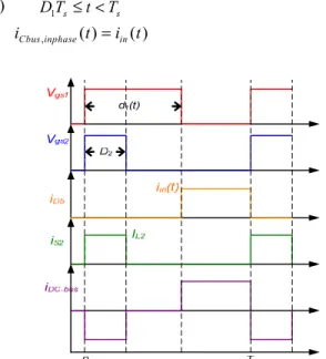
In-phase control means no energy from the input flows directly into the rear stage; therefore, the current ripple of the DC-bus capacitor is high. The detailed operation of the converter with in-phase control is described in the following. Fig. 4 shows waveforms of the in-phase control.
Mode I(t = t0 ~ t1): In this mode, S1 and S2 are both turned
on; D5 and D6 are both turned off, as shown in Fig. 5(a). In this condition, L1 stores energy from Vin, and L2 stores energy from the DC-bus capacitor. This mode ends when S2 is turned off.
Mode II(t = t1 ~ t2): In this mode, S1 is turned on and S2 is
turned off; D5 is turned off and D6 is turned on, as shown in Fig. 5(b). In this condition, L1 stores energy from Vin, and L2 releases energy to the output. Additionally, there is no current flowing into the DC-bus capacitor. This mode ends when S1 is turned off.
Mode III(t = t2 ~ t3): In this mode, S1 and S2 are turned off;
D5 and D6 are turned on, as shown in Fig. 5(c). In this condition, L1 releases energy to the DC-bus capacitor, and L2 releases energy to the output. This mode ends when S1 and S2 are turned on.
B. Interleaved Control
Fig. 6 shows waveforms of the converter in interleaved control. The detailed operation of the proposed converter in interleaved control is described in the following.
Fig. 4. Waveforms of in-phase control.
(a) Mode I
(b) Mode II
(c) Mode III
Fig. 5. Operating mode of the in-phase control.
Mode I(t = t0 ~ t1): In this mode, S1 is turned on and S2 is
turned off; D5 is turned off and D6 is turned on, as shown in Fig. 7(a). In this condition, L1 stores energy from Vin, and L2 releases energy to the output. Also, no current flows into the
DC-bus capacitor. This mode ends when S2 is turned on.
Mode II(t = t1 ~ t2): In this mode, S1 and S2 are turned on; D5
and D6 are turned off, as shown in Fig. 7(b). In this condition,
L1 stores energy from Vin and L2 stores energy from the DC-bus capacitor. This mode ends when S1 is turned off.
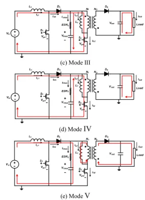
Mode III(t = t2 ~ t3): In this mode, S1 is turned off and S2 is
turned on; D5 is turned on and D6 is turned off, as shown in Fig. 7(c). In this condition, L1 releases energy to the rear stage and the DC-bus capacitor, and L2 stores energy from the front stage. This mode ends when the current of the DC-bus capacitor is 0.
Mode IV(t = t3 ~ t4): In this mode, S1 is turned off and S2 is
turned on; D5 is turned on and D6 is turned off, as shown in Fig. 7(d). In this condition, L1 releases energy to the rear stage, and L2 stores energy from the front stage and the DC-bus capacitor. This mode ends when S2 is turned off.
Mode V(t = t4 ~ t5): In this mode, S1 and S2 are both turned
off; D5 and D6 are both turned on, as shown in Fig. 7(e). In this condition, L1 releases energy to the DC-bus capacitor, and L2 releases energy to the output. This mode ends when S1 is turned on.
Fig. 6. Waveforms of the interleaved control.
(a) Mode I
(b) Mode II
(c) Mode III
(d) Mode IV
(e) Mode V
Fig. 7. The operation of the interleaved control
III. MATHEMATICAL ANALYSIS OF THE DC-BUSCAPACITOR
CURRENT RIPPLE
The reduction of the DC-bus capacitor current ripple is proved by mathematical analysis [3]. Hence, the analysis of the current ripple in these two control methods described above is shown as follows.
Before analysis, some assumptions should be made. Except for the assumption in Section II (D2 > (d1(t)-0.5) ), the input power factor is well controlled to unity. Therefore,
( ) sin( ) in in v t =V ωt ,and (1)
( )
sin( )
in ini t
=
I
ω
t
(2)The front-stage PFC operates in CCM, and the inductor current
iL1(t) is proportional to the input voltage vin(t). First, the voltage-conversion ratio can be derived in relation to the topologies used. The conversion ratio of the front-stage PFC in boost is 1 ( ) 1 ( ) in Cbus v t V d t = −
,
(3)and vin(t) and d1(t) change continuously. For simplicity, the average current of L1 in the boost topology is the same as the input current following AC input voltage, as follows:
1 ( )
L in
I =i t
.
(4)Additionally, the average current of L2 in the flyback converter is IL2. The analysis of in-phase control is discussed first. Assume its origin is at the beginning of a particular switching period. There are three intervals in the current ripple of the DC-bus capacitor of in-phase control, as shown in Fig. 8.
(I) 0≤ <t D T2 s , ( ) 2 Cbus inphase L i t = −I (5) (II) D T2 s ≤ <t D T1 s , ( ) 0 Cbus inphase i t = (6)
(III) D T1 s≤ < t Ts
, ( ) ( )
Cbus inphase in
i t =i t (7)
Fig. 8. Simplified waveforms of the DC-bus capacitor current ripple with in-phase control.
The average square value of the ripple current of the DC-bus
capacitor with in-phase control, 2
, ( ) Cbus inphase i t , over one switching cycle is 2 2 2 2 , , 2 2 1 1 ( ) s ( ) ( )[1 ( )] s t T
Cbus inphase T t Cbus inphase L in
s
i t i t dt I D i t d t
T
+
< > =
∫
= + − (8)Combining (1) and (3) and substituting (2) into (8) yield the following expression: 2 2 2 2 , 2 2 sin ( ) sin s in Cbus inphase T L in Cbus V t i t I D I t V ω ω < > = + . (9)
And then the rms value of the current ripple of DC-bus capacitor with in-phase control is
2 , , 0 , 1 ( ) ac s T
Cbus inphase rms Cbus inphase T ac i i t dt T =
∫
< > 2 2 2 2 2 0 sin 1 ( sin ) ac T in L in ac Cbus V t I D I t dt T V ω ω =∫
+ 2 2 2 2 4 3 in L in Cbus V I D I V π = + (10)where Tac is the duration of the input AC voltage.
Now the analysis of interleaved control is discussed. Assume its origin is at the beginning of a particular switching period. There are four intervals in the current ripple of the DC-bus capacitor of interleaved control, as shown in Fig. 9. (I) 0 2 s T t ≤ < ( ) 0 Cbus i t = (11) (II) 1( ) 2 s s T t d t T ≤ < 2
( )
Cbus Li
t
= −
I
(12) (III) 1( ) s 2s 2 s T d t T ≤ <t +D T 2 ( ) ( ) Cbus in L i t =i t −I (13) (IV) 2 2 s s s T D T t T + ≤ <( )
( )
Cbus ini
t
=
i t
(14)Fig. 9. Simplified waveforms of the DC-bus capacitor current ripple with interleaved control.
The average square value of the DC-bus capacitor ripple current with interleaved control, 2( )
Cbus
i t , over one switching cycle is 2( ) 1 s 2( ) s t T Cbus T t Cbus s i t i t dt T + < > =
∫
2 2 2 2 1 2 2 1 2 1 1 1 [ ( ) ] [ ( ) ] [ ( )] ( )[ ] 2 2 2 L in L in I d t i t I D d t i t D = − + − + − + − 2 2 2 2 1 2 2 1 1 ( )[1 ( )] 2 ( ) [ ( )] 2 L in in L I D i t d t i t I D d t = + − − + −.
(15)Substituting (1) , (2) and (3) into (15) to yields the following expression: 2 2 2 2 2 2 2 2 sin 2 sin ( ) s sin sin (1 2 ) in in Cbus T L in L in Cbus Cbus V t V t i t I D I t I I t D V V ω ω ω ω < > = + + − −
(16) The rms value of the DC-bus capacitor current ripple with
interleaved control is 2 , 0 1 ac ( ) s T Cbus rms Cbus T ac i i t dt T =
∫
< > 2 2 2 2 2 2 2 0 sin 2 sin 1 Tac[ sin in sin (1 2 in )] L in L in ac Cbus Cbus V t V t I D I t I I t D dt T V V ω ω ω ω =∫
+ + − − 2 2 2 2 2 2 2(1 2 ) 4 [ ] 3 in in L in L in Cbus Cbus V V D I D I I I V V π −π = + − − (17)where Tac is the period of the input AC voltage.
Squaring and comparing (10) and (17), it is clear that the current ripple of DC-bus capacitor with interleaved control is lower, as 2 2(1 2 ) 0 in Cbus V D V π − − >
.
(18)As a result, the DC-bus capacitor current ripple can be reduced by interleaved control.
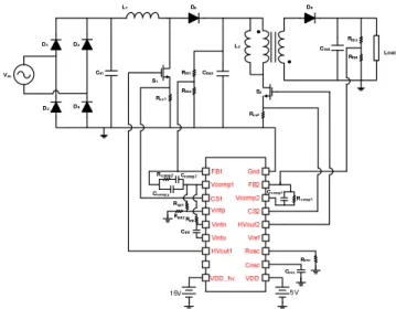
IV. CIRCUIT DESIGN
10. There are five control-function blocks required in this controller. The functions of these blocks are discussed in the following.
Fig. 10. Block diagram of the proposed controller.
A. Frequency Divider
The Clk signal is used to control the operating frequency of the converter. Moreover, using the Clk divided by the frequency divider can generate two interleaved Clk signals to effectively achieve interleaving of the front and rear stages.
Fig. 11 illustrates the positive-edge trigger D flip-flop [6]. Besides, two AND gates are also included. This control block produces two interleaved clock signals, Clk1 and Clk2. The Clk produced by the oscillator becomes two interleaved signals. Thus, there are two interleaved signals AND the Clk signal. Fig. 12 reveals the waveforms of the oscillator and the two interleaved clock signals, Clk1 and Clk2.
Fig. 11. Frequency divider.
Fig. 12. Waveforms of oscillator and frequency divider.
B. One-Cycle Controlled PFC Modulation
One-cycle control was proposed in the beginning of the 1990s [7]. This approach can be utilized to control DC-DC converters, audio-frequency power amplifiers, active power filters, and for power-factor correction (PFC) [8]. In this thesis, one-cycle control is used to achieve the front-stage PFC. Fig. 13 illustrates the ideal equivalent model of PFC [9]. The relationship between input voltage and current seems to be resistive, as follows: g g e v i R = , (19)
where ig is the average of rectified line current, vg is the rectified line voltage, and Re is the emulated resistance. A notation M(d) is denoted as the voltage-conversion ratio, as follows: ( ) O g V M d v = , (20)
where VO is the output voltage. Because of time-variant vg, the duty ratio of the power-factor corrector is always changing. Fortunately, because the switching frequency of the power-factor corrector is usually much higher than the line frequency,
vg can be approximated as constant in consecutive switching cycles. Therefore, all quantities of the power-factor corrector can be approximated with steady-state values. In the following, a boost-type power-factor corrector is taken as an example to show the derivation procedures. Some characteristics of the boost converter are declared below [8].
1 ( ) 1 M d d = − (21)
Substituting (19) and (20) into (21) yields
(1 )
O e g
V −d =R i . (22)
Because R is an imaginary value, a sensing resistance e R is S
used to displace R , as follows: e
(1 ) m S g v −d =R i , (23) where S m O e R v V R
= is defined as the modulation voltage.
Additionally, iT = ≈iL iL , where iL is the current of the inductance and iL=ig for the boost converter [10][11].
(1 ) m S T v −d =R i (24) 2 ( ) ( ) g e v t p t R = ( ) g v t O V e R ( ) g i t i to( )
Fig. 13. Equivalent model of power-factor corrector.
Fig. 14 illustrates a one-cycle controlled PFC circuit. For fitting equation (24), only half the quantity of the current signal is needed in the proposed control circuit. Fig. 15 shows the modulation waveforms of the proposed one-cycle controlled PFC in this controller.
m v 2 S T R i (1 ) 2 m v d −
(1 ( )) 2 m v d t − s d T s T ( ) 2 S T R i t⋅
Fig. 15. Modulation waveforms of the proposed one-cycle controlled PFC in this controller.
C. Current-Mode PWM Control Block
In this proposed controller, current-mode control is used in the rear DC-DC stage. The current-mode PWM control block is illustrated in Fig. 16 [14]. The FB2 is a feedback signal divided by the resistor sensing the output voltage of the rear-stage DC-DC converter. The OTA, which is used to amplify the error between FB2 and Vref20, and the compensation
networks composed of external components, Zc, introduce a
voltage level. Additionally, there is another feedback signal, CS2, that is proportional to the current of the switch. CS2 compared with the output of OTA, Vota, provides a signal to
the pulse generator turning off the switch. A clock signal Clk2 generated by an oscillator and frequency divider sets the pulse generator and turns on the switch every switching cycle.
Fig. 16. The current-mode PWM control block.
Fig. 17 reveals the waveforms of current-mode control. The Clk2 signal controls the pulse generator to initiate the switching period, causing Q2 to be high and turning the switch on. While the switch conducts, the CS2 signal proportional to the current of the switch current increases with a positive slope that depends on the value of inductance and the regulator voltages. Eventually, the current signal CS2 becomes equal to the control signal Vota. At this point, the output signal of the
comparator in Fig. 16 is high and resets the pulse generator to turn off the switch.
0 t
Vota
Clk2
CS2
Q2
Fig. 17. Waveforms of current-mode PWM control block.
V. LAYOUT AND SIMULATION RESULTS
A. Layout
The layout of the proposed IC is shown in Fig. 18. The proposed IC is fabricated with TSMC 0.25 UM CMOS
high-voltage process. The control function parameters can be adjusted by external components. The area of the core of this controller including pads is 0.9×0.9 mm2.
Fig. 18. Layout of the proposed IC.
B. Simulation Results
The topology shown in Fig. 19 is chosen as Section II. The front stage is a boost PFC, and the rear stage is a flyback converter. Table 1 reveals the circuit parameters.
As Fig. 20 and Fig. 21 show, the voltage of the DC bus and the output voltage meet the specifications. The voltage of the DC bus is about 390 V, and the output voltage is about 12 V. The interleaved control and the in-phase control have no effect on either the voltage of the DC bus or the output voltage.
Fig. 19. The chosen topology with the proposed controller. Table 1. Circuit parameters of the chosen topology.
Parameter Value Unit
Input Voltage 110 Vrms Output Voltage 12 V Rated Power 150 W Operating Frequency, fs 100 kHz Cin 100 nF L1 1 mH Cbus 220 μF L2 900 μH N1/N2 20 Cout 2200 μF
Fig. 20. The voltage of the DC bus.
Fig. 21. The output voltage.
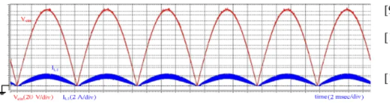
Fig. 22, 24, 26 and Fig. 28 show waveforms of the DC-bus capacitor current ripple with interleaved control in three different Vcbus conditions. And Fig. 23, 25, 27 and Fig. 29 show waveforms of the DC-bus capacitor current ripple with in-phase control in three different Vcbus conditions. Using interleaved control, part of the current of the front stage flows directly into the rear stage. Therefore, the DC-bus capacitor current ripple with interleaved control is lower than that with in-phase control. Zone 2 and Zone 4 are the best of improving ripple reduction. Table 2 reveals the rms value of the DC-bus capacitor current ripple at different levels of input voltage.
Fig. 22. The current ripple of Cbus with interleaved control (zone1).
Fig. 23. The current ripple of Cbus with in-phase control (zone1).
Fig. 24. The current ripple of Cbus with interleaved control (zone2).
Fig. 25. The current ripple of Cbus with in-phase control (zone2).
Fig. 26. The current ripple of Cbus with interleaved control (zone3).
Fig. 27 .The current ripple of Cbus with in-phase control (zone3).
Fig. 28. The current ripple of Cbus with interleaved control (zone4).
Fig. 29. The current ripple of Cbus with in-phase control (zone4).
Table2. DC-bus capacitor current ripple with different control methods. Input Voltage In-Phase Control Interleaved Control Reduction Ratio
110 Vrms 1.14 A 0.89 A 28%
According to the function of the one-cycle controlled PFC modulation described in Section IV, Fig. 30 reveals the simulated achievements of one-cycle control. The spike in the current-sensing signal is due to the reverse-recovery of D5. Fig.
31 shows the waveforms of steady-state operation. The input is AC 110 Vrms and the output power is 150 W in this example.
By applying Fourier analysis to the input current, power factor (PF) and total harmonic distortion (THD) at full-load condition can be obtained. The values of PF and THD are 0.99 and 2.3%, respectively. Also, Fig. 32 reveals the spectrum of the input current at full-load condition.
Fig. 31. Waveforms of rectified input voltage and current in steady-state operation. 0 0.5 1 1.5 1 3 5 7 9 Harmonic order Ha rm oni c am pli tu de (Nor m al iz ed )
Fig. 32. Harmonic contents of input current.
VI. CONCLUSION
This thesis implements a constant-frequency interleaved control between the front-stage PFC and the rear-stage DC-DC. The front-stage PFC is controlled by one-cycle control and the rear stage is controlled by current-mode control. The simulation results show that the current ripple of the DC-bus capacitor is reduced with interleaved control. The THD of the input current in the front-stage PFC is lower than 2.3% at 110 Vrms/150 W, and the PF of the input current in the front stage
PFC is 0.99 at 110 Vrms/150 W.The output voltage is stable
and meets the specifications.
ACKNOWLEDGMENTS
The authors gratefully acknowledge financial support from the National Science Council of Taiwan under project No. 101-3113-P-006-024, and chip implementation support from National Chip Implementation Center, Taiwan.
REFERENCES
[1] M. J. Kocher and R. L. Steigerwald, “An AC-to-DC converter with high quality input waveforms,” IEEE Trans. on Industry Applications, vol. IA-19, no. 4, July 1983, pp. 586-599.
[2] N. Mohan, T. M. Undeland and W. P. Robbins, Power Electronics, John Wiley & Sons, Inc., 2003.
[3] Masahito Shoyama, Toshiaki Kurachi, and Tamotsu Ninomiya, “Ripple current analysis of an electrolytic capacitor in power factor correctors,” Electronics and Communications in Japan, Part2, Vol. 79, No. 4, 1996. [4] K. N. Leung and P. K. T. Mok, “A sub-1-V 15-ppm/°C CMOS bandgap
voltage reference without requiring low threshold voltage device,” IEEE Journal of Solid-state circuits, vol. 37, no. 4, April 2002, pp. 526-529. [5] C. F. Lee, and K. T. Mok, “A monolithic current-mode CMOS DC-DC
converter with on-chip current-sensing technique” IEEE Journal of Solid-state circuits, vol. 39, no. 1,Jan. 2004, pp. 3-14.
[6] M. Afghahi and J. Yuan, “Double edge triggered D-flip-flops for high speed CMOS circuit,” IEEE Journal of Solid-state circuits, vol. 26, no. 8, Aug. 1991, pp. 1168-1170.
[7] Z. Lai and K. M. Smedley, “A new extension of one-cycle control and its application to switching power amplifiers” IEEE Transactions on Power Electronics, vol. 11, no. 1, Jan. 1996, pp. 99-105.
[8] Z. Lai and K. M. Smedley, “A family of continuous-conduction-mode power-factor-correction controllers based on the general pulse-width modulator” IEEE Transactions on Power Electronics, vol. 13, no. 3, May 1998, pp. 501-510.
[9] R. W. Erickson, and D. Maksimovic, Fundamental of Power Electronics, 2nd ed., Kluwer Academic Pub., 2001.
[10] D. Maksimovic, Y. Jang and R. Erickson, “Nonlinear-carrier control for high power factor boost rectifiers,” IEEE Applied Power Electronics Conference, March 1995, pp. 635-641.
[11] Z. Lai and K. M. Smedley, “A general constant-frequency pulsewidth modulator and its applications,” IEEE Transactions on Circuits and Systems, vol. 45,no. 4, April 1998, pp. 386-396.
[12] D. Ma, W. H. Ki, and C. Y. Tsui, “An integrated one-cycle control buck converter with adaptive output and dual loops for output error correction,” IEEE Journal of Solid-State Circuits, vol. 39, no. 1, Jan. 2004.
[13] R. Mammano, Switching Power Supply Topology Voltage Mode vs. Current Mode, Texas Instruments, June 27, 1994.