Closed Loop Control of a Symmetrical Multipulse Modulated Single-Phase Bi-directional AC
Regulator Feeding an Inductive Load
A. N. Arvindan and E. Karthik
Electrical and Electronics Engineering Department, S.S.N. College of Engineering,
Chennai, India [email protected]
Abstract—Single-phase topology of the bi-directional a.c. chopper with power MOSFET embedded discrete component four- quadrant switch (4QSW) realizations that operate in a high frequency chopping mode is used to implement the symmetrical multipulse modulation (SMM) technique that provides ac power control. The technique involves generation of several equidistant pulses per half cycle (M) and control of their duty cycle (δ) that are necessary for gate control of the 4QSWs and regulation of the fundamental output voltage magnitude. The output voltage magnitude and its harmonic profile are dependent on the values of M and δ. In this paper a novel practical closed loop feedback based analog-digital control is implemented and presented that provides SMM compliant pulses that can be manipulated for M and δ. Relevant experimental results are furnished to demonstrate the efficacy of the proposed control.
Keywords-ac chopper; duty cycle; four-quadrant switch;
harmonic profile; symmetrical multipulse modulation
I. INTRODUCTION
Limitations associated with thyristorised ac controllers comprising inverse-parallel connected thyristors include a lagging power factor even for resistive load, the rather large turn-on and turn-off times of the thyristors that inhibit their deployment for high frequency applications and adoption of advanced pulse-width modulation (PWM) techniques that need multiple switching (turn-on and turn-off) within a half cycle, requirement of commutation circuits with bulky elements etc.
These limitations are addressed by deploying self-commutating devices that facilitate adoption of the symmetrical multipulse modulation (SMM) in ac controllers. In this paper single-phase topology of the symmetrical multipulse modulated bi- directional ac regulator, comprising power MOSFET embedded four-quadrant switches (4QSWs), with closed loop control of the output voltage, catering to an inductive load is presented. A novel analog-digital feedback based control mechanism is used to implement the SMM [1] technique that continues to evoke interest [2] and involves generation of several equidistant pulses per half cycle (M) used to obtain an output voltage that can be continuously varied by varying M and the duty cycle (δ) of the pulses is proposed. The SMM strategy is well ensconced and the analyses, undertaken over a
Figure 1. Power MOSFET embedded four-quadrant switch realizations.
period of time, of the chopped output voltage waveform for harmonic content for various values of M and δ reveal its efficacy in terms of elimination [1]-[5] and selective reduction [6]-[7] of the lower order harmonics and, hence its superiority [8]-[11] over phase-control. The proposed control mechanism is capable of controlling the output voltage by either varying the parameters M and δ individually or simultaneously, apart from rendering operation at high frequency chopping (more pulses per half cycle (M)) facilitating easy and economical filtration.
II. TOPOLOGICAL CONSIDERATIONS OF BI-DIRECTIONAL PWM AC REGULATOR
A. Power Semiconductor Devices for PWM AC Regulators Bi-directional AC regulators provide power flow control in both half cycles thus necessitating the use of four-quadrant switches (4QSWs) i.e. switches capable of blocking bi-polar voltages and controlling the instants of conduction and non- conduction of bi-directional current. 4QSWs are commercially not yet available and therefore their functionality is obtained by realizations [12] that comprise diodes and power transistors as depicted in Fig. 1. The development and advancement in semiconductor technology has resulted in availability of power transistors at ratings that are compatible with medium power applications. Power MOSFETs have the highest switching frequency of the three categories of transistors viz. BJTs, IGBTs, and MOSFETs considered for deployment in ac power
control applications and, therefore, are most viable for PWM strategy based control that entails multiple switching of power semiconductor devices within every half cycle of the source voltage. Apart from possessing the self-commutating property typical of transistors, the power MOSFET has several desirable facets in that it is voltage controlled, has high input impedance that simplifies its gate drive circuit and enables drawing of very low gate current which in turn facilitates negligible gate power relative to its power rating, has a negative temperature coefficient, is not susceptible to the second breakdown phenomenon unlike the power BJTs and because it is a unipolar device, i.e. it uses only the majority carriers in conduction, it has no delays because of storage or recombination of minority carriers during turn-off. MOSFETs, have limited power-handling capacity, however, at low power and high frequency applications, they are used with unsurpassed performance because of higher switching rate and negligible losses.
B. Enhancement-Type MOSFET based 4QSW Realizations The enhancement-type MOSFETs are used in converters as switching devices rather than the depletion-type because at zero gate voltage, the former remain off while the latter remain on. The n-channel enhancement-type MOSFET, used in the 4QSW realizations in this paper as shown in Fig. 1, is the fastest power switching device, with switching frequency greater than 1 MHz, and is available with voltage and current ratings as high as 600 V and 40 A respectively. Operation of power-switching devices at higher frequencies results in decreased size and weight of output transformers, inductors, and filter capacitors that facilitates compact and economical
Figure 2. Single-phase bi-directional pulse width modulated ac regulator.
power electronic systems. The power MOSFET has a parasitic diode which permits current flow in the opposite direction. An external diode oriented opposite to the parasitic diode is connected in series with the MOSFET to negate the parasitic diode effect and confers on it the reverse voltage blocking ability. Thus, the series combination of a diode and MOSFET functions as a two-quadrant switch (2QSW). Each 4QSW realization is an inverse-parallel connection of two 2QSWs.
III. SYMMETRICAL MULTIPULSE MODULATED SINGLE- PHASE BI-DIRECTIONAL AC REGULATOR
The single-phase topology of the symmetrical multipulse modulated (SMM) ac regulator with two 4QSWs –one in series with the voltage source and the other across the load is shown in Fig. 2. The gate control signals for the MOSFETs, as per the SMM PWM technique, are shown in Fig. 3. Fig. 4 shows the
0 0.01 0.02 0.03
0V 330V
-330V
T ime (Secs.) VsS1S2S1'
0 0 01 0 02 0 03
S2'
0V 10V
10V 0V
0V 10V 10V 0V
Figure 3. Gate signals of the MOSFETs in an symmetrical multipulse modulated ac regulator with M = 9 and δ=0.5 feeding an inductive load.
0 0.01 0.02 0.03 0.04 0.05 0.06 0.07 0.08
-200 -100 0 100 200 330
-330
Time (in Secs.)
Output voltage, Vo (V) and current, io (A)
Vo io
Figure 4. Output (load) voltage and current waveforms, for M=9 and δ=0.5, of the pwm ac regulator feeding a purely inductive load.
0.04 0.045 0.05 0.055 0.06 0.065 0.07 0.075 0.08 -200
330
-330 -100 0 100 200
T ime (in Secs.)
Output voltage, Vo (V)
0.04 0.045 0.05 0.055 0.06 0.065 0.07 0.075 0.08
-3 -2 -1 0 1 2 3
T ime (in Secs.)
Output current, io (A)
Figure 5(a). Output voltage, Vo, for M = 9 and δ = 50%. Figure 5(b). Output current, io, for M = 9 and δ = 50%.
Figure 5. Output (load) voltage and current waveforms, for M=9 and δ=0.5, of the pwm ac regulator feeding an inductive (RL) load.
output (load) voltage (Vo), and current (io) waveforms corresponding to the gate control logic depicted in Fig. 3, when the SMM ac regulator is feeding a purely inductive load. From Fig. 3 it is clear that the symmetrical multipulse modulation (SMM) technique involves periodic multiple switching of the relevant device in series with the load at a frequency that is determined by the desired number of output voltage pulses per half cycle (M). The switching frequency (fsw) is given by
fsw = 2Mfs, (1)
wherein, fs = frequency of the ac voltage source (Vs) which is also the fundamental frequency of Vo. The device connected in inverse-parallel with the series switching device is kept in the turned-on condition throughout the relevant half cycle. The devices across the load have a switching frequency = fs and have gating signals that are complementary to each other. The rms value of Vo is controlled by varying the duty cycle (δ) of the pulses and M.
Figs. 4 and 5 depict load waveforms associated with purely inductive (L = 10 mH) and RL (R = 110 Ω and L = 55 mH) loads respectively for the same gating logic pertaining to M = 9 and δ = 0.5 and magnitudes of Vs = 325.27 V (peak) and fs = 50 Hz shown in Fig. 3. From Figs. 4 and 5 it is evident that the load voltage and current waveforms are very different for L and RL loads. It has been verified by the authors that in the case of the purely inductive load the wave shape of the load current (io) remains independent of the magnitude of the load inductance (L) for the range L = 5 mH to 55 mH. The effect of
change in the load inductance magnitude within this range on io
is limited to changing its magnitude. From Fig. 4 it is clear that it takes two cycles i.e. 40 ms for Vo and io to overcome transients and attain successive symmetric half cycles corresponding to steady state. It is also obvious that the switching of the relevant device is redundant resulting in non- chopped portions of Vo and io during regeneration i.e. when Vo
is positive and io is negativeand vice-versa. The modes of operation within a cycle and sub-modes within an half cycle pertaining to bi-directional power transfer between a single- phase ac source and an inductive load with explicit details of the devices involved have already been reported [11].
Figs. 5(a) and 5(b) show Vo and io respectively for two cycles of steady state operation attained after 40ms for RL load. The current (io) is saw-toothed and uneven because of dissipation of energy in the load resistor during free-wheeling and there are small time intervals of regeneration as well. It is noteworthy that io is continuous in Figs. 4 and 5(a) indicative of adequate load inductance.
IV. CLOSED LOOP CONTROL
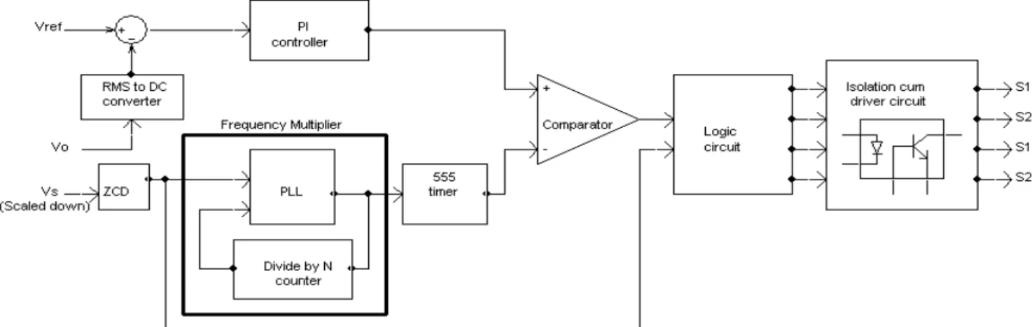
The schematic diagram of the control circuit used to produce the gating signals for the power MOSFETs is shown in Fig. 6. The objective of the closed loop control depicted in Fig.
6 is to obtain a smooth variation of the magnitude of the rms value of the output voltage (Vo) in the 0 to Vs(rms) range, where Vs(rms) = rms value of the source voltage (Vs), and maintain that magnitude i.e. voltage regulation of (Vo). This is accomplished
Figure 6. Block diagram of the closed loop control.
Figure 7. Generation of duty cycle modulated signal by PI control.
Figure 8. Generation of high frequency pulse by PLL frequency multiplier.
by controlling M and δ, the key parameters in SMM. The parameters M and δ, however, have to be judiciously varied because their manipulation not only controls Vo but also its harmonic profile. The control technique involves the generation of a duty cycle (δ) modulated pulse signal via a proportional and integral controller that is compared with a 555 timer generated sawtooth waveform synchronized with a pulse train, produced by a phase locked loop based frequency multiplier, that has a frequency almost equal to the switching frequency, fsw. The output signal of this comparison that has the requisite δ and frequency, fsw, is fed to a two-input digital logic circuit. The output signal of the zero crossing detector (ZCD) of Vs, having frequency fs is used for synchronizing the control signals and is given as the second input to the logic circuit. The logic circuit outputs the gating signals, as per the SMM technique shown in Fig. 3, to the four MOSFETs via the isolation cum driver circuits.
A. Generation of Duty Cycle Modulated Control Signal The output voltage, Vo, is appropriately scaled down and a dc signal equivalent to its rms value is obtained via the rms-to- dc converter (AD636) that is compared with the reference signal, Vref, by a difference amplifier which provides the error signal. This error signal is given to a proportional and integral (PI) controller that outputs a duty cycle (δ) modulated control signal.
The analog hardware implementation of the scheme to
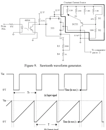
Figure 9. Sawtooth waveform generator.
Figure 10. Signals associated with sawtooth waveform generation generate the duty cycle modulated pulse train is shown in Fig.
7. It comprises four operational amplifiers A1, A2, A3 and A4 that function as difference amplifier, proportional controller, integral controller and inverting summer respectively. In Fig. 7 Vdo (rms) is the dc equivalent of the scaled down rms value of Vo. B. Generation of High FrequencyPulse Train Using Phase
Locked Loop Frequency Multiplier
Three ICs, CD4046BC micropower phase-locked loop (PLL), HEF4059B a programmable divide-by-N counter and 4050 CMOS buffer are interconnected as shown in Fig. 8 to obtain a pulse train of high frequency, Nfs. The PLL has an edge-controlled digital memory network, phase comparator II (CP II) and a linear voltage controlled oscillator (VCO). CP II provides a digital error signal and lock-in signal to indicate a locked condition maintaining a 0° phase shift between signal input and comparator input while the VCO produces an output signal (pin 4) whose frequency is determined by the voltage at its input (pin 9), and the capacitor and resistors connected to pin C1A, C1B, R1 and R2. The 4059 is used to divide an input frequency by any number N from 3 to 15999. The value of N is set by jam inputs J1 – J16 and mode select pins Ka, Kb and Kc. C. Generation of Sawtooth Waveform
The output of the PLL (pin 4), is a high frequency (Nfs) pulse train that is given to the optocoupler (4N26) at the input of the 555 timer based saw tooth generator circuit shown in Fig. 9 via the 4050 buffer shown in Fig. 8. The input (at pin 2) and output (across the capacitor) signals of the 555 timer in Fig. 9 are depicted in Fig. 10. From Figs. 9 and 10 it is evident
that the 555 timer is operated in linear ramp generation mode that produces a ramp signal of time period, T, whenever the input signal at pin 2 goes low. The input signal has a time period, Ts, given by
Ts = 1/Nfs. (2)
From (2) it is clear that the PLL shown in Fig. 8 multiplies the input frequency fs provided by theZCD by N, the value set in the divide-by-N counter.
The ramp generating mechanism in Fig. 9 is simple. The capacitor is charged by a constant current source which causes the voltage across it to be a linear ramp. The 555 timer is used to keep a tab on the voltage across the capacitor and discharge it when it reaches Vm. The amplitude of the ramp, Vm, depends on the voltage in pin 5. Resistors R3 and R4 are used to fix this value. The time period, T, depends on the value of the capacitor and the resistor connected to the emitter of the PNP transistor. Their value is chosen in such a way that T ≈ Ts. This ensures that the high frequency sawtooth (linear ramp) signal derived from the high frequency (Nfs)pulse train signal is in synchronization with the time intervals of the half cycles pertaining to the source voltage frequency, fs. Switch S1 is used to connect different values of resistors to the emitter to change the frequency of the ramp.
D. Generation of Gate Control Signals
The generation of gate control signals compliant with symmetrical multipulse modulation (SMM) involves processing and conditioning of the signals generated earlier. It is important to note that PLL frequency multiplier and ZCD circuits are at 5V levels whereas PI controller, sawtooth waveform generator, and logic circuit operate at 12V. Hence, the PLL’s and the ZCD’s outputs are translated from 0-5V to 0-12V using the 4N26 optocoupler.
1) High speed voltage comparator: The duty cycle (δ) modulated signal obtained from the PI control circuit shown in Fig. 7 and the high frequency sawtooth signal obtained from the 555 timer circuit in Fig. 9 are applied to the inverting and non-inverting input terminals respectively of the LM311 operational amplifier that is used as a high speed voltage comparator. The output of the amplifier is a voltage signal that is δ modulated, PI controlled and of frequency as per (2).
2) Digital Logic based signal conditioning: The output of the LM311 amplifier and the ZCD output signal that provides the time intervals corresponding to the two half cycles of Vs
continually, when an appropriately scaled down Vs is applied at its input, are applied to a combinational logic to obtain SMM compliant pulses. The SMM compliant pulses for M = 9 and δ = 0.5 are shown in Fig. 3. The values of M and δ can be varied by changing the parameters of the various control signal generating circuits. The generation of the SMM compliant pulses for MOSFETs S1, S2, S1' and S2' corresponding to the single-phase topology, shown in Fig. 2, by the combinational digital gate logic is illustrated in Fig. 11.
The pulses shown in Fig. 11, however, are not given to the MOSFETs directly but via gate driver circuits.
Figure 11. Combinational logic for generating gate signals.
E. Isolation and Gate Driver Circuits
Individual 4N26 optocouplers are provided for each MOSFET to provide the requisite isolation between the control and power circuitry. They are also used for interfacing and coupling systems of different potentials and impedances as already stated. A 1K resistor is used to limit the current flowing through the IR LED because of the input control signal. The phototransistor is powered by an independent 12V source.The output is taken across a 3.3K resistor connected to the emitter.
V. EXPERIMENTAL RESULTS AND DISCUSSIONS The experimental results pertaining to the proposed closed loop control of the single-phase topology with type I 4QSWs are presented in this section. The technique is applicable to the other two types of 4QSWs as well. In fact, the gate signals for type I 4QSWs realizations can be used for type II ones as well, while deployment of type II 4QSW realizations greatly simplifies the logic circuit as only two gate signals that are phase shifted by 180° i.e. inverted w.r.t. each other are required.
A. Control Signals
The δ modulated signal at the output of the PI controller is shown in Fig. 12. The signal at the input (pin 2) of the 555 timer in the sawtooth wave generator is depicted in Fig. 13.
Figure 12. Output signal of PI controller.
Figure 13. Input signal at the 555 timer of the sawtooth generator.
Figure 14. Linear ramp signal at the output of the sawtooth generator.
Figure 15. Input and output signals of the 555 timer based sawtooth generator.
Figure 16. Gate signals for series MOSFETs, S1 and S2.
Figure 17. Gate signals for shunt MOSFETs, S’1 and S’2.
Fig. 14 shows the high frequency ramp generated by the sawtooth generator. The input and output signals of the generator are shown together in Fig. 15. Figs. 16 and 17 show the gate pulses for the series and shunt MOSFETs respectively for M = 9 and δ = 0.5.
B. Output Waveforms
Figs. 18 and 19 depict the output (load) voltage and current respectively for M = 9, δ = 50%, for an inductive load with R = 110Ω, and L = 55mH, Vs = 325.27 V (peak) and fs = 50Hz. The waveforms in Figs. 18 and 19 agree well with the theoretical estimates shown in Figs. 5(a) and 5(b) respectively.
VI. CONCLUSION
A novel analog-digital closed loop control of the single-
Figure 18. Output voltage, Vo, for M = 9 and δ = 50%.
Figure 19. Output current, io, for M = 9 and δ = 50%.
phase symmetrical multipulse modulated ac regulator with four-quadrant switch realizations feeding an inductive load is proposed that includes a PLL based frequency multiplier. The theoretical design of the control technique is practically realized by its implementation in a prototype. Experimental results confirm its efficacy.
ACKNOWLEDGMENT
A. N. Arvindan, thanks his undergraduate students Mr.
Prithvin Rajendran and Mr. K. Balakumaran for their help in the fabrication of the experimental set up and recording data.
REFERENCES
[1] K. E. Addoweesh and A. L. Mohamadein, “Microprocessor based harmonic elimination in chopper type AC voltage regulators,” IEEE Trans. Power Electron., vol. 5, pp. 191-200, Apr.1990.
[2] G. M. Hashem and M. K. Darwish, “Generalized symmetrical angle PWM technique for ac voltage controller,” in Proc. IEEE UPEC’04, 2004, pp.898-901.
[3] G. H. Choe, A. K. Wallace, and M. H. Park, “An improved PWM technique for AC choppers,” IEEE Trans. Power Electron., vol. 4, no. 4, pp. 496-505, Oct. 1989.
[4] D. H. Jang and G. H. Choe, “A new APWM technique with harmonic elimination and power factor control in AC choppers,” in Proc. IEEE IECON’92, 1992, pp.252-258.
[5] K. Sundareswaran and A. P. Kumar, “Voltage harmonic elimination in PWM AC chopper using genetic algorithm,” IEE Proceedings Electric Power Applications, vol.151, No.1, pp. 26-31, Jan.2004.
[6] K. A. Krishnamurthy, G. K. Dubey, and G. N. Revankar, “AC-DC and AC-AC converter control with selective reduction of line harmonics,” in Proc., Inst. Electr. Eng., 1978, 125, (11), pp.1269-1272.
[7] D. A. Deib and H. W. Hill, “Optimal harmonic reduction in ac/ac chopper converters,” in Proc. IEEE PESC’93, 1993, pp. 1055-1060.
[8] A. N. Arvindan, V. K. Sharma and M. Subbiah, “Harmonic Analysis of Microprocessor based Three-Phase Improved Power Quality AC/AC Voltage Controller using Power MOSFETs,” in Proc. IEEE ISIE’06, 2006, pp.763-768.
[9] A. N. Arvindan and V. K. Sharma, “Microprocessor based Symmetrical Multipulse Modulation in a Three-Phase Improved Power Quality AC- AC Converter using Four Quadrant Switch Realizations” in the IETE Journal of Research (ISSN 0377-2063), Vol 53, No. 6, Nov.- Dec.2007, pp 563-571.
[10] A. N. Arvindan, “Power Quality Assessment in a Bi-directional AC/AC Converter with Four-Quadrant Switch Realizations” in Proc. IEEE TENCON’08, 2008.
[11] A. N. Arvindan, V. K. Sharma and M. Subbiah, “Selective Harmonic Elimination in a Microprocessor based Single-Phase AC Chopper with Four Quadrant Switch Realizations” in Proc. of India International Conference on Power Electronics, IEEE-IICPE’06, 2006, pp. 51-56.
[12] T. A. Lipo, “Recent progress in the Development of Solid-State AC Motor Drives,” IEEE Trans. Power Electron., vol. PE-3, No.2, pp. 105- 117, April 1988.