semiconductor (SONOS) devices with embedded silicon nanocrystals (Si-NCs) in silicon nitride using in situ method with multilevel and 2-b/cell operation have been successfully demonstrated. The proposed in situ Si-NC deposition method exhibits the advantages of low cost, simplicity, and compatibility with modern IC processes. SONOS memories with embedded Si-NCs exhibit a significantly improved performance with a large memory window (> 5.5 V), low operating voltage (P/E voltage: Vg= 6 V, Vd = 7 V and Vg=−7 V, Vd = 10 V,
respectively), greater tolerable gate and drain disturbance (Vt
shift < 0.2 V), negligible second-bit effect, high P/E speed (after programming time = 10 μs with a 2-V shift of Vt under
Vg = Vd= 6 V operation), good retention time (> 108 s for
13% charge loss), and excellent endurance performance (after 104P/E cycles with a memory window of 3 V).
Index Terms—In situ, memory window, nonvolatile memory, retention time, silicon nanocrystal (Si-NC).
I. INTRODUCTION
T
HE SCALING down of conventional floating-gate mem-ory devices has met limitations beyond 60-nm node technology [1]. Tunneling oxide thickness below 7 nm must confront a number of challenges, including large stress-induced leakage current (SILC), serious short-channel effect, and crit-ical floating-gate coupling effect [2]–[4]. The most serious issue among these challenges is the increase of the tunneling oxide leakage current induced by program/erase cycling stress, resulting in data retention degradation when the tunneling oxide is scaled below 7 nm [3].Recently, metal–oxide–semiconductor (MOS) memory de-vices with embedded silicon nanocrystals (Si-NCs) and polysilicon–oxide–nitride–oxide–semiconductor (SONOS) non-volatile memory devices have attracted attention because of their potential for solving the issues involved in scaling down conventional floating-gate memory devices [5]–[8]. In MOS
Manuscript received October 2, 2009; revised April 5, 2010; accepted May 19, 2010. Date of publication June 28, 2010; date of current version July 23, 2010. This work was supported by the National Science Council, Taiwan, under Contract NSC-97-2221-E-009-152-MY3. The review of this paper was arranged by Editor H. S. Momose.
T.-Y. Chiang, Y.-H. Wu, P.-Y. Kuo, K.-T. Wang, C.-C. Liao, C.-R. Yeh, and T.-S. Chao are with the Department of Electrophysics, National Chiao Tung University, Hsinchu 300, Taiwan (e-mail: [email protected]).
W. C.-Y. Ma is with the Institute of Electronics, National Chiao Tung University, Hsinchu 30010, Taiwan.
W.-L. Yang is with the Department of Electronic Engineering, Feng Chia University, Taichung 40724, Taiwan.
Color versions of one or more of the figures in this paper are available online at http://ieeexplore.ieee.org.
Digital Object Identifier 10.1109/TED.2010.2051489
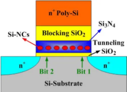
Fig. 1. Schematic representation of a Flash memory cell structure with the nitride film embedded Si-NCs using the in situ method.
memories with embedded Si-NCs and SONOS memories, charge stored in the trapping layer offers advantages over floating-gate memories, including high density, elimination of drain-induced turn-on effect, 2-b operation, no floating-gate coupling effect, and excellent immunity to SILC [9]–[12]. When the tunneling oxide thickness is scaled down below 7 nm, SONOS memories show much better retention than floating-gate memories. This is attributed to the discrete and deep-level storage states of SONOS memory devices.
However, SONOS memories still face many issues, including lateral stored charge migration, the second-bit effect, and erase saturation [13]–[16]. Therefore, a MOS memory device with embedded Si-NCs has been proposed to solve lateral stored charge migration and second-bit effect [17], [18]. Unfortu-nately, it is difficult to grow high-density suitably distributed uniformly sized Si-NCs on silicon oxide. It has been reported that the density of Si-NCs on silicon nitride is higher than on oxide [19], [20], because silicon nitride exhibits lower activation energy and higher nucleation growth rate than oxides. This means that nucleation occurs more easily on silicon nitride surfaces than on silicon oxide surfaces.
The performance of SONOS can be improved further if em-bedded Si-NCs are used. The Si-NCs can be formed in Si-rich SiNxlayers using different chemical vapor deposition (CVD)
techniques or by a low-energy Si ion implantation technique [21], [22]. Finding a simple scheme to produce embedded Si-NCs in silicon nitride has thus become increasingly impor-tant for the development of SONOS-type memories.
Recently, we have investigated SONOS-type memory de-vices with ex situ embedded Si-NCs in nitride, showing im-proved performance in terms of larger memory window, lower operation voltage, and longer retention time [23]. However, this growth method of Si-NCs is not an in situ method. Later, we successfully developed an in situ method to fabricate SONOS devices with embedded Si-NCs in silicon nitride [24]. In this
Fig. 2. 1× 1 μm2AFM image of Si-NCs formed on the nitride film with the four deposition conditions. The highest density of the Si-NC is 9× 1011cm−2.
paper, a SONOS-type Flash memory with in situ embedded Si-NCs in silicon nitride is fully investigated in detail, includ-ing dot size and density analyzed by AFM and transmission electron microscopy (TEM). The performance and reliabil-ity of devices formed with different Si-NC deposition times (10, 30, 60, and 90 s), including data retention, multilevel and 2-b operation, P/E cycling test, and drain and gate disturbance, were investigated.
II. EXPERIMENTALPROCEDURE
Fig. 1 shows the schematic diagram of the in situ embedded Si-NCs in a silicon nitride film. Devices were fabricated on p-type (100) 150-mm 8–12-Ω· cm silicon substrates. After the
LOCOS isolation process, a 2.5-nm-thick tunneling oxide was thermally grown in N2O on the silicon substrate. The formation of in situ embedded Si-NCs in the silicon nitride film includes three steps, including bottom nitride, Si-NCs, and top nitride. In the first step, i.e., the forming of the bottom silicon nitride, a 3-nm-thick silicon nitride film was deposited in a low-pressure CVD system using NH3 (130 sccm) and SiCl2H2 (30 sccm) at 780 ◦C. The second step was the in situ forming of the Si-NCs. It is noted that wafers were still in the same tube at the same temperature. The only change in the recipe was turning off the NH3 gas and reducing the flow rate of the SiCl2H2to 10 sccm. In this step, the Si-NCs were then in situ deposited on the wafers. The deposition times used were 10, 30, 60, and 90 s, respectively. As previously mentioned, the density of
Fig. 3. Top view of an HR-TEM image of 30-s deposition time embedded the nitride film with in situ Si-NC.
Si-NCs deposited on the nitride is higher than that on oxide. Hence, this method enjoys the advantage of high density of Si-NCs. The final step in the process is the formation of the top nitride, with a thickness of 4 nm, on the Si-NCs deposited in the same tube by turning on the NH3gas again.
Using this approach, the wafers do not need to change tubes during the process of embedding the Si-NCs in the silicon nitride layer. These Si-NCs can be easily in situ embedded into the silicon nitride without additional instruments or treatments. All three steps were executed in the same tube and at the same temperature by the alternating on/off switching of NH3 gas. A blocking oxide (20 nm) was deposited on the nitride using a high-density plasma CVD system. An n+-poly-Si (200 nm) was deposited as the control gate. Subsequently, gate patterning, source/drain implantation, contact patterning, and the remaining standard CMOS processes were completed to fabricate the SONOS-type memory with in situ embedded Si-NCs in the silicon nitride layer.
III. RESULTS ANDDISCUSSION
Fig. 2 shows the 1× 1 μm2AFM images of Si-NCs formed on the nitride film with the four deposition conditions. The highest density of the Si-NC is 9× 1011cm−2. The root-mean-square roughness values of the SONOS with Si-NC deposition for 10, 30, 60, and 90 s are 0.499, 0.548, 0.453, and 0.517 nm, respectively. These Si-NCs are well separated, with an average 2-D distance > 5 nm on the silicon nitride, which ensures electrical isolation between any two Si-NCs. Fig. 3 shows the top view of a high-resolution TEM (HR-TEM) image for Si-NCs. The mean size of Si-NCs and the aerial density turned out to be 7–12 nm and 7−9 × 1011 cm−2, respectively. The trends of the size and the density of Si-NCs across various deposition times are shown in Fig. 4. A longer deposition time results in a larger Si-NC size. However, the longest deposition time (90 s) of Si-NCs does not show the highest density.
Fig. 4. Si-NC size and density depend on the deposition time.
Fig. 5. Program and erase speed characteristics for 30-s deposition time at different operating voltages.
Instead, the 60-s deposition time shows the highest density among these samples. This may be attributed to the merging of NCs during a longer deposition time. After comprehensive material and morphological analysis of the Si-NCs, a series of electrical characterizations was then carried out to discover the optimum conditions for programming and erasing SONOS with
in situ embedded Si-NCs.
Fig. 5 shows the programming speed of a SONOS-type memory with in situ Si-NCs for a deposition time of 30 s under different operating bias conditions. The memory window is defined as the change of the Vt of the sample between the
programmed and erased states. The threshold voltage (Vt) is
defined as the applied gate voltage when the drain current is 100 nA during operation mode. The device is programmed by using channel hot-electron injection and erased by using band-to-band hot-hole injection. When Vd and Vg were both set at
6 V, a considerably high programming speed (t = 10 μs) with a 2-V shift of Vtwas found. A higher voltage of Vdand Vgtends
to result in faster programming speed and larger programming window. It should be noted that the saturation phenomenon of programming window did not occur when the voltage bias was set at Vg= Vd= 7 V. Fig. 6 shows the curves of programming
(Vg= Vd= 6 V) and erasing speed (Vg=−8 V, Vd = 8 V)
across the different deposition times of Si-NCs. A deposition time of 30 s results in faster programming and erasing speeds than the other times due to the maximum trapping cross area, a product of dot size and dot density. This implies that higher dot size and density will increase the number of trapping states, which can be located in Si-NCs or at the interface of the
Fig. 6. Program and erase speed curves of the same operating voltage across different Si-NC deposition times.
Fig. 7. Data retention characteristics of a Si-NC Flash memory device across different deposition times at a programming window of 4 V at room tempera-ture (inset shows a programming window of 2 V at 150◦C).
silicon nitride and the Si-NCs. Among all devices, those with a deposition time of 10 s show the minimum memory window having the smallest and lowest density Si-NCs. This implies that a 10-s deposition time is not enough for the formation of higher density Si-NCs.
Fig. 7 shows the data retention performance measured at room temperature. The charge loss can barely be observed up to 104s. At room temperature, the charge loss was below 13%, as extrapolated to 108s. The retention characteristics of devices baked at 150◦C are measured and shown in the inset of Fig. 7. They exhibit only a 10% charge loss for 104 s. Compared to conventional SONOS, SONOS memories with embedded Si-NCs appear to have better data retention due to the additional trapping sites created at the Si-NCs or at the interface of the Si-NCs and the nitride. Fig. 8 shows the data retention behavior of the SONOS memory devices with embedded Si-NCs and multilevel operation at room temperature and high temperature (at 85◦C). There is negligible charge loss for multilevel opera-tion for SONOS memory devices with embedded Si-NCs.
The band-to-band tunneling is the main cause of drain dis-turbance, resulting in charge injection into the trapping nitride layer [25], [26]. The electrons can be migrated by vertical hopping in the silicon nitride layer. The electrons can move to the bottom silicon nitride from the top silicon nitride to increase the total quantity of trapped electrons, resulting in a larger memory window. The result means that the deposition time of 30 s has a lot of effective trapped states. Therefore, the deposition time of 30 s has a larger gate and drain disturbance. However, the drain disturbance and gate disturbance of SONOS
Fig. 8. Multilevel operation data retention of Si-NC memories for the deposi-tion time of 30 s at room temperature and high temperature (at 85◦C).
Fig. 9. Drain disturbance and gate disturbance characteristics of various Si-NC embedded nitride layer memory samples.
Fig. 10. Id–Vgcurves of the 2-b Si-NC embedded nitride film memory in one
cell; forward read and reverse read for programmed bit 1.
memories with embedded Si-NCs for different deposition times are not affected at all, as shown in Fig. 9. The Vtshifts of the
drain disturbance and gate disturbance were less than 0.2 V for devices with different deposition times after 103s under stress. As a result, the drain disturbance and gate disturbance can be ignored for devices with embedded Si-NCs.
Fig. 11. Two-bit effect characteristics of various Flash memory samples using in situ Si-NCs.
Fig. 10 shows the feasibility of performing a 2-b operation for the SONOS memory with embedded Si-NCs for a depo-sition time of 30 s through a forward read and reverse read scheme in a single cell. The read operation was achieved using a reverse read scheme. From the Id–Vg curves, it is evident
that the forward and reverse reads can be employed to detect the information stored in programmed bit 1 (drain side). The memory window difference between the forward and reverse
Vt’s was found to be 2 V, indicating that 2-b operation in a single cell is possible. Table I summarizes the operation bias conditions for the 2-b operation of SONOS memory with embedded Si-NCs. Forward read and reverse read after pro-gramming at the drain-side storage result in a memory window of 2 V, as shown in Fig. 11. A well-behaved 2-b operation was found for the SONOS with a 30-s deposition time, most likely because a deposition time of 30 s generates the optimum size and aerial density of Si-NCs. These results confirmed again that MOS memory devices with embedded Si-NCs can solve the lateral stored charge migration and second-bit effect [17], [18] in long-channel devices, but this improvement on charge migration needs more investigations in short-channel devices. Fig. 12 shows the endurance characteristics of the SONOS memories with embedded Si-NCs. The programming and erasing conditions were Vg= 6 V and Vd= 7 V for 30 μs
and Vg=−7 V and Vd= 10 V for 20 ms, respectively. A large
memory window, i.e., 3 V, was obtained for a deposition time of 30 s after 104 P/E cycles. The deposition time of 10 s is not shown in Fig. 12 because the Vt cannot shift under this
operation voltage. The upward Vtshift is due to interface trap
generation and electron trapping in the tunneling oxide during P/E cycle operation [27], [28]. After 104P/E cycles, the charge loss curves of the SONOS memories with embedded Si-NCs are measured at room temperature and are shown in Fig. 13. A large memory window of 2.7 V and a small charge loss
Fig. 12. Endurance characteristics of Si-NC embedded nitride layer memories across different samples up to 104P/E cycles.
Fig. 13. Data retention after 104P/E cycles in different samples of embedded Si-NCs in nitride layer memories.
of 12% are found as the time of stress is increased to 104 s at room temperature. The memory window was still 2.3 V, as extrapolated to 108 s. Before P/E cycles, the Icp currents of the device with embedded Si-NC deposition for 30, 60, and 90 s are 7.43× 10⁻⁹, 7.59× 10⁻⁹, and 1.1× 10⁻⁹ nA, respectively. After 104P/E cycles, the Icpcurrents of the device with embedded Si-NC deposition for 30, 60, and 90 s are 1.2× 10⁻⁸, 1.26× 10⁻⁸, and 1.59× 10⁻⁸, respectively. The device with a deposition time of 30 s has the lower Icpcurrent, which means lower interface state after 104 P/E cycles. This result means that the deposition time of 30 s has lower charge loss due to better interface states. The charge loss appears to result from detrapping from shallow traps at the interface or/and electron traps in the tunneling oxide. Some memory devices with high-k material such as Si-NCs, Si3N4, La2O3, CeO2, and Y2O3 [29]–[33] are compared in Table II. Among these devices, SONOS memories with embedded Si-NCs exhibit large memory windows at a lower operating voltage. SONOS memories also have a higher program/erase speed and excellent data retention at high temperatures and after P/E cycles compared to the devices with high-k materials. This is due to the newly created trapping sites in the Si-NCs or at the interface of the silicon nitride and the Si-NCs.
IV. CONCLUSION
SONOS-type Flash memory devices with in situ embedded Si-NCs in nitride have been successfully demonstrated. Multi-level and 2-b/cell operations of this device are easily obtained with a fast program/erase speed. It is found that the optimum
time of deposition of Si-NCs is 30 s based on the program/erase speed and endurance performance. This device has been shown to have excellent electrical performance in terms of larger memory windows, fast program/erase speed, ignored second-bit effect, almost negligible drain and gate disturbance, long data retention times, and good endurance up to 104cycles with a memory window of 3 V. This in situ scheme to incorporate Si-NCs in nitride appears to be very promising for SONOS Flash memory applications.
ACKNOWLEDGMENT
The authors would like to thank the National Nano Device Laboratories and the Nano Facility Center of National Chiao Tung University for the processes support.
REFERENCES
[1] The International Technology Roadmap for Semiconductors (ITRS), p. 232006.
[2] R. Degraeve, F. Schuler, B. Kaczer, M. Lorenzini, D. Wellekens, P. Hendrickx, M. van Duuren, G. J. M. Dormans, J. Van Houdt, L. Haspeslagh, G. Groeseneken, and G. Tempel, “Analytical percolation model for predicting anomalous charge loss in Flash memories,” IEEE Trans. Electron Devices, vol. 51, no. 9, pp. 1392–1400, Sep. 2004. [3] K. Naruke, S. Taguchi, and M. Wada, “Stress induced leakage current
limiting to scale down EEPROM tunnel oxide thickness,” in IEDM Tech. Dig., 1988, pp. 424–427.
[4] M. H. White, Y. Yang, P. Ansha, and M. L. French, “A low volt-age SONOS nonvolatile semiconductor memory technology,” IEEE Trans. Compon., Packag., Manuf. Technol., vol. 20, no. 2, pp. 190–195, Jun. 1997.
[5] J. D. Blauwe, “Nanocrystal nonvolatile memory devices,” IEEE Trans. Nanotechnol., vol. 1, no. 1, pp. 72–77, Mar. 2002.
[6] R. Ohba, N. Sugiyama, K. Uchida, J. Koga, and A. Toriumi, “Nonvolatile Si quantum memory with self-aligned doubly-stacked dots,” IEEE Trans. Electron Devices, vol. 49, no. 8, pp. 1392–1398, Aug. 2002.
[7] P. Xuan, M. She, B. Harteneck, A. Liddle, J. Bokor, and T.-J. King, “FinFET SONOS Flash memory for embedded applications,” in IEDM Tech. Dig., 2003, pp. 609–613.
[8] C. W. Oh, S. D. Suk, Y. K. Lee, S. K. Sung, J. D. Choe, S. Y. Lee, D. U. Choi, K. H. Yeo, M. S. Kim, S. M. Kim, M. Li, S. H. Kim, E. J. Yoon, D. W. Kim, D. Park, K. Kim, and B. I. Ryu, “Damascene gate FinFET SONOS memory implemented on bulk silicon wafer,” in IEDM Tech. Dig., 2004, pp. 893–896.
[9] M. She and T. J. King, “Impact of crystal size and tunnel dielectric on semiconductor nanocrystal memory performance,” IEEE Trans. Electron Devices, vol. 50, no. 9, pp. 1934–1940, Sep. 2003.
[10] M. Takata, S. Kondoh, T. Sakaguchi, H. Choi, J.-C. Shim, H. Kurino, and M. Koyanagi, “New nonvolatile memory with extremely high density metal nano-dots,” in IEDM Tech. Dig., 2003, pp. 553–556.
[11] M. K. Cho and D. M. Kim, “High performance SONOS memory cells free of drain turn-on and over-erase: Compatibility issue with current Flash technology,” IEEE Electron Device Lett., vol. 21, no. 8, pp. 399–401, Aug. 2000.
[12] T. Y. Chan, K. K. Young, and C. Hu, “A true single-transistor oxide–nitride–oxide EEPROM device,” IEEE Electron Device Lett., vol. EDL-8, no. 3, pp. 93–95, Mar. 1987.
[13] Y. K. Lee, T. H. Kim, S. H. Lee, J. D. Lee, and B. G. Park, “Twin-bit silicon–oxide–nitride–oxide–silicon (SONOS) memory by inverted sidewall patterning (TSM-ISP),” IEEE Trans. Nanotechnol., vol. 2, no. 4, pp. 246–252, Dec. 2003.
[14] E. Lusky, Y. Shacham-Diamand, I. Bloom, and B. Eitan, “Electrons reten-tion model for localized charge in oxide–nitride–oxide (ONO) dielectric,” IEEE Electron Device Lett., vol. 23, no. 9, pp. 556–558, Sep. 2002. [15] W. J. Tsai, N. K. Zous, C. J. Lie, C. C. Liu, C. H. Chen, and T. Wang,
“Data retention behavior of a SONOS type two-bit storage Flash memory cell,” in IEDM Tech. Dig., 2001, pp. 719–722.
[16] T. Sugizaki, M. Kobayashi, M. Minakata, M. Yamaguchi, Y. Tannura, Y. Sugiyama, T. Nakanishi, and H. Tanaka, “Novel multi-bit SONOS type flashing memory using a high-k trapping layer,” in VLSI Symp. Tech. Dig., 2003, pp. 27–28.
[17] S. K. Samanta, P. K. Singh, W. J. Yoo, G. Samudra, Y. C. Yeo, L. K. Bera, and N. Balasubramanian, “Enhancement of memory window in short channel non-volatile memory devices using double layer tungsten nanocrystals,” in IEDM Tech. Dig., 2005, pp. 170–173.
[18] Y. H. Lin, C. H. Chien, C. T. Lin, C. Y. Chang, and T. F. Lei, “Novel two-bit HfO2nanocrystal nonvolatile Flash memory,” IEEE Trans. Electron
Devices, vol. 53, no. 4, pp. 782–789, Apr. 2006.
[19] T. Baron, F. Martin, P. Mur, C. Wyon, M. Dupuy, C. Busseret, A. Souifi, and G. Guillot, “Low pressure chemical vapor deposition growth of silicon quantum dots on insulator for nanoelectronics devices,” Appl. Surf. Sci., vol. 164, no. 1–4, pp. 29–34, Sep. 2000.
[20] T. Baron, F. Martin, P. Mur, C. Wyon, and M. Dupuy, “Silicon quantum dot nucleation on Si3N4, SiO2and SixNysubstrates for nanoelectronic
devices,” J. Cryst. Growth, vol. 209, no. 4, pp. 1004–1008, Feb. 2000. [21] K. S. Cho, N. M. Park, T. Y. Kim, K. H. Kim, G. Y. Sung, and J. H. Shin,
“High efficiency visible electroluminescence from silicon nanocrystals embedded in silicon nitride using a transparent doping layer,” Appl. Phys. Lett., vol. 86, no. 7, p. 071 909, Feb. 2005.
[22] S. Choi, H. Choi, T. W. Kim, H. Yang, T. Lee, S. Jeon, C. Kim, and H. Hwang, “High density silicon nanocrystal embedded in SiN pre-pared by low energy (< 500 eV) SiH4 plasma immersion ion
implantation for non-volatile memory application,” in IEDM Tech. Dig., 2005, pp. 166–169.
for multi-level and 2-bit/cell operation for wrapped-select-gate (WSG) SONOS memory,” Semicond. Sci. Technol., vol. 23, no. 1, p. 015 004, Jan. 2008.
[27] G. Puzzilli and F. Irrera, “Data retention of silicon nanocrystal storage nodes programmed with short voltage pulses,” IEEE Trans. Electron De-vices, vol. 53, no. 4, pp. 775–781, Apr. 2006.
[28] J. Sarkar, S. Dey, D. Shahrjerdi, and S. K. Banerjee, “Vertical Flash memory cell with nanocrystal floating gate for ultradense integration and good retention,” IEEE Electron Device Lett., vol. 28, no. 5, pp. 449–451, May 2007.
[29] C. Y. Ng, T. P. Chen, M. Yang, J. B. Yang, L. Ding, C. M. Li, A. Du, and A. Trigg, “Impact of programming mechanisms on the performance and reliability of nonvolatile memory devices based on Si nanocrystals,” IEEE Trans. Electron Devices, vol. 53, no. 4, pp. 663–667, Apr. 2006. [30] J. L. Wu, C. H. Kao, H. C. Chien, C. Y. Wu, and J. C. Wang,
“Deposition-temperature effect on nitride trapping layer of silicon– oxide–nitride–oxide–silicon memory,” Jpn. J. Appl. Phys., vol. 46, no. 5A, pp. 2827–2830, 2007.
[31] Y. H. Lin, C. H. Chien, T. Y. Yang, and T. F. Lei, “Two-bit lanthanum oxide trapping layer nonvolatile Flash memory,” J. Electrochem. Soc., vol. 154, no. 7, pp. H619–H622, 2007.
[32] S. M. Yang, C. H. Chien, J. J. Huang, T. F. Lei, M. J. Tsai, and L. S. Lee, “Cerium oxide nanocrystals for nonvolatile memory applications,” Appl. Phys. Lett., vol. 91, no. 26, pp. 262 104-1–262 104-3, Dec. 2007. [33] T. M. Pan and W. W. Yeh, “High-performance high-k Y2O3SONOS-type
Flash memory,” IEEE Trans. Electron Devices, vol. 55, no. 9, pp. 2354– 2360, Sep. 2008.
Tsung-Yu Chiang was born in Yunlin, Taiwan, in
1984. He received the B.S. degree in physics from National Chung Cheng University, Chiayi, Taiwan, in 2006. He is currently working toward the Ph.D. degree in the Department of Electrophysics, National Chiao Tung University, Hsinchu, Taiwan.
His research interest includes the studies of semi-conductor device physics, including low-temperature polycrystalline-silicon thin-film transistors, metal-gate/high-k technology, strain techniques, and non-volatile Flash memories.
Yi-Hong Wu was born in Chiayi, Taiwan, in 1984.
He received the B.S. and M.S. degrees in electronics engineering from Feng Chia University, Taichung, Taiwan, in 2006 and 2008, respectively. He is cur-rently working toward the Ph.D. degree in the De-partment of Electrophysics, National Chiao Tung University, Hsinchu, Taiwan.
His research interest includes the studies of semi-conductor device physics, including low-temperature polycrystalline-silicon thin-film transistors and non-volatile Flash memories.
Po-Yi Kuo was born in Pingtung, Taiwan, in 1978.
He received the Ph.D. degree in electronics engineer-ing from National Chiao Tung University, Hsinchu, Taiwan, in 2007.
Since October 2008, he has been with the De-partment of Electrophysics, National Chiao Tung University, as a Postdoctoral Researcher. His current research topics are gate-all-around nanowire tran-sistors, vertical channel thin-film trantran-sistors, Si/Ge heterojunction devices, floating-body-effect random-access memories, and tunneling field-effect thin-film transistors.
Kuan-Ti Wang was born in Kaohsiung, Taiwan,
in 1983. He received the B.S. degree in electronics engineering from Chang Gung University, Taoyuan, Taiwan, in 2006. He is currently working toward the Ph.D. degree in the Department of Electrophysics, National Chiao Tung University, Hsinchu, Taiwan.
His research interests include dynamic threshold MOSFETs, metal-gate/high-k technology, and non-volatile Flash memories.
Chia-Chun Liao was born in Taoyuan, Taiwan, in
1980. He received the B.S. degree in electrophysics from National Chiao Tung University, Hsinchu, Taiwan, in 2007, where he is currently working toward the Ph.D. degree in the Department of Electrophysics.
His research interests include strain techniques, PEALD for metal-gate/high-k applications, and non-volatile Flash memories.
Chi-Ruei Yeh was born in Taipei, Taiwan, in 1985.
He received the M.S. degree in electrophysics from National Chiao Tung University, Hsinchu, Taiwan, in 2009.
He is currently with the Department of Electrophysics, National Chiao Tung University. His research interests include low-temperature polycrystalline-silicon thin-film transistors and metal-gate/high-k technology.
Program of Industrial R&D. He is currently a Professor with the Department of Electronic Engineering. He is an Independent Director of the Solid State System Company, Ltd. (Flash Disk Innovators), and is an Advisory Counselor of the Anova Technology Company, Ltd. He is interested in Flash (SONOS), metal silicides, Cu and low-k-dielectric multilevel interconnections, and bio-electronics.