Raman analysis of longitudinal optical phonon-plasmon coupled modes
of aligned ZnO nanorods
An-Jen Cheng,1Yonhua Tzeng,1,2Hui Xu,3Siddharth Alur,3Yaqi Wang,3Minseo Park,3,a兲 Tsung-hsueh Wu,4Curtis Shannon,4Dong-Joo Kim,5and Dake Wang6
1
Alabama Microelectronics Science and Technology Center, Department of Electrical and Computer Engineering, Auburn University, Auburn, Alabama 36849, USA
2Institute of Microelectronics, Department of Electrical Engineering, National Cheng Kung University, Tainan 70101, Taiwan
3Department of Physics, Auburn University, Auburn, Alabama 36849, USA
4Department of Chemistry and Biochemistry, Auburn University, Auburn, Alabama 36849, USA 5Materials Research and Education Center, Department of Mechanical Engineering, Auburn University, Auburn, Alabama 36849, USA
6Department of Physics, Furman University, Greenville, South Carolina 29613, USA
共Received 15 September 2008; accepted 2 February 2009; published online 3 April 2009兲 The electronic properties of vertically aligned ZnO nanorods have been investigated using micro-Raman spectroscopy. The concentration and mobility of the charge carriers were determined via Raman line shape analysis using longitudinal-optical-phonon-plasmon coupled mode. The local laser heating and the stress effects have been considered when analyzing the Raman spectra. The mobility and carrier concentration of the aligned ZnO nanorods are 84.8 cm2/V s and 3.8 ⫻1017cm−3, respectively. As a comparison, the mobility and carrier concentration of the undoped bulk ZnO were also obtained from the Raman line shape analysis. The mobility of the aligned ZnO nanorods is about 20% lower than that of the undoped bulk ZnO, which can be attributed to enhanced surface scattering due to the reduction in dimension. © 2009 American Institute of Physics.关DOI:10.1063/1.3093877兴
INTRODUCTION
Recently, one-dimensional共1D兲 semiconductor nanorods have been considered as promising building blocks for nano-scale photonic devices and circuits.1–3Among these semicon-ductor nanorods, 1D zinc oxide 共ZnO兲 is one of the most intensively studied nanorod materials. ZnO is a wide band-gap semiconductor which possesses a direct band band-gap of 3.37 eV and a room temperature exciton binding energy of 60 meV. ZnO has been considered a promising candidate for subwavelength waveguides, ultraviolet 共UV兲 laser diodes, UV photodetectors, white light emitting diodes, solar cells,4 and other types of optoelectronic devices. Room temperature stimulated excitonic emission and optically pumped laser ac-tion are observed from high quality ZnO thin film, which makes ZnO a suitable candidate for UV laser applications.5,6 It is also expected that an exciton-based ZnO laser performs better than its GaN counterpart.7
It is significantly important to characterize the electronic properties of the 1D ZnO nanorods if one would want to fabricate the nanorod-based electronic and optoelectronic de-vices with a desired performance. Electrical characterization techniques such as Hall,8 capacitance-voltage 共C-V兲, and impedance9 measurements are being used to measure the electronic parameters such as carrier concentration. How-ever, these techniques require preparation of electrical con-tact to a material under investigation. On the other hand, optical measurement techniques such as Raman spectroscopy
can provide a noncontact method for the measurement of the electronic parameters. Optical methods are more useful than its electrical counterpart when analyzing a low-dimensional materials system due to the difficulty in the preparation of the contact to nanostructures.
By exploiting the coupling between longitudinal-optical 共LO兲 phonons and plasmons in polar semiconductors, the electronic parameters of materials can be extracted via Ra-man spectroscopy. In polar semiconductors, the long-range electrostatic Coulombic force mediates the coupling of LO phonons and the plasmons, resulting in the formation of two hybrid excitations of the longitudinal-optical-phonon-plasmon共LPP兲 modes. The LPP modes influence the energy exchange between carrier and the lattice, thus playing an important role in carrier relaxation and transport.10–14 The relative energy shift and linewidth broadening of the LPP modes are directly influenced by the concentration and the mobility of free charge carriers. Both LPP modes 共high-frequency and low-共high-frequency LPP modes兲 can be observed if the damping of plasmon is sufficiently small. However, only the high-frequency LPP modes can be observed when plas-mon damping is significant.
Gallium arsenide共GaAs兲 is the first semiconducting ma-terial from which the LPP modes have been observed by Raman spectroscopy.15 Previously, the electronic parameters of GaN thin film and nanorods have been determined by using Raman spectroscopy.16,17 However, this method has not been applied in determining the electronic parameters of ZnO nanostructures. Therefore, in this work, we have col-lected LPP modes of ZnO nanorods and determined the free
a兲Author to whom correspondence should be addressed. Electronic mail:
carrier concentration and electron mobility of the sample. As a comparison, the LPP modes collected from a single crystal bulk ZnO wafer was also investigated.
EXPERIMENT
Vertically aligned ZnO nanorods were grown on a p-Si substrate using thermal chemical vapor deposition 共CVD兲. An ultrathin layer共with thickness of ⬃20 nm兲 of zinc was sputtered on the p-type Si substrate prior to the ZnO nanorod synthesis. As-sputtered samples were loaded into the furnace at a temperature of 400 ° C and were annealed for 8 h at 1 atm in order to oxidize Zn layer to form ZnO. All the samples were ultrasonically cleaned in pure methanol for 10 min, followed by immersion of the samples in methanol with a suspension of zinc nanopowder for an additional 30 min. No special catalysis was used in nanorod growth. All the as-prepared samples were loaded on top of an alumina boat containing Zn powder. Meanwhile, an additional alu-mina boat containing Zn powder was inserted into the end of a smaller quartz tube before loading the alumina boat, which has the sample on it. Then, the temperature of the CVD reactor was elevated to 500 ° C with a ramping rate of 5 ° C/min. Argon 共Ar兲 and oxygen 共O2兲 were used as the carrier and reactant gases, respectively, for ZnO nanorod growth. The flow rates of Ar and O2were 88 and 8 SCCM 共standard cubic centimeter per minute兲, respectively. The growth of ZnO nanorods were performed at 50 Torr for 60 min.
The surface morphologies of the samples were studied using a field-emission scanning electron microscope共JOEL JSM-7000兲. The crystal structures of the samples were char-acterized by x-ray diffraction共XRD兲 using a Rigaku Miniflez powder x-ray diffractometer with Cu K␣ radiation. Micro-photoluminescence and micro-Raman spectroscopy were performed at room temperature using 325 and 441.6 nm la-ser lines, respectively, from a He–Cd lala-ser 共Kimmon Elec-tric兲 with a spectrometer 共Jobin-Yvon兲 integrated with a grat-ing 共3600 lines/mm groove density兲. Both spectra were collected using a spectrometer with a thermoelectrically cooled charge coupled device detector. Backscattering geom-etry was used for Raman scattering measurement. The spec-tral resolution of the grating is 0.2 cm−1.
RESULTS AND DISCUSSION
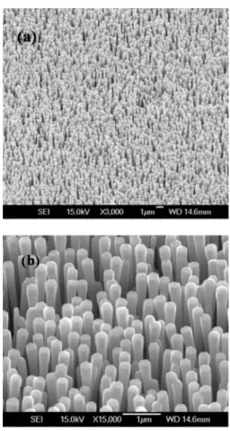
The scanning electron microscope共SEM兲 images of the vertically aligned ZnO nanorods synthesized using thermal CVD are shown in Fig. 1. The low magnification SEM shown in Fig.1共a兲reveals that the well-aligned ZnO nano-rods were uniformly grown on a relatively large area of the p-type Si substrate. Figure 1共b兲 shows the high-resolution SEM image of the ZnO nanorods. The hexagonally shaped nanorods with an average diameter of 100– 150 nm can be clearly observed. The XRD pattern shown in Fig.2also re-veals high crystallinity and c-axis preferential orientation of the ZnO nanorods. Only the XRD peaks corresponding to 共0002兲 and 共0004兲 planes can be seen.
The photoluminescence共PL兲 spectrum of ZnO exhibits a near band edge共NBE兲 UV emission peak and a broad visible
emission band due to the deep level intrinsic and/or extrinsic defects.18,19 The mechanism of the broad visible emission, especially the blue-green emission, was explained to be me-diated by oxygen vacancies 共VO兲, i.e., singly ionized20 or doubly ionized oxygen vacancy.21 The PL spectrum of the aligned ZnO nanorods is shown in Fig.3. A strong UV NBE emission is observed at 382 nm and no visible luminescence was collected. This result possibly implies that our aligned ZnO nanorods are free of optically active defects since no broad visible emission is observed.
Thermodynamically stable ZnO crystallite possesses a wurtzite structure and belongs to the space group of C64v.
FIG. 1.共a兲 Low magnification and 共b兲 high magnification SEM micrographs of aligned ZnO nanorods.
Group theory predicts that the material with the C64v space group is expected to have A1共z兲+2B1+ E1共x,y兲+2E2 optical phonon modes at the⌫ point of the Brillouin zone.22Among these optical phonon modes, A1 mode is both infrared and Raman active and is polarized in the z direction. E1mode is also infrared and Raman active, but the phonon is polarized in the xy plane. The two B1modes are silent and the two E2 modes are only Raman active. A1 and E1 are the two polar modes which can be influenced by the long-range macro-scopic electric field. Raman modes that can be observed in a spectrum are strongly dependent on the Raman selection rules, which take into consideration the orientation of the crystal with respect to the directions of propagation and po-larization of the incident and Raman scattered light.
Since the z共-,-兲zគ backscattering geometry was employed and the c axis of ZnO is along the z direction, only the Raman peaks of A1共LO兲, E2共1兲, and E2共2兲modes are allowed according to the Raman selection rule. According to the se-lection rule, ZnO nanorods must be grown along the c axis for pure A1共LO兲 mode collection. If the nanorods are tilted with a certain angle, quasimodes produced by mode mixing can be collected. The phonon frequency of the quasi-LO mode lies in between those of E1共LO兲 and A1共LO兲 modes. The frequency of quasi-LO mode 共QLO兲 can be described using the following equation:
QLO2 =E12 共LO兲sin2+A12 共LO兲cos2, 共1兲 whereis the angle between the c axis and the direction of phonon propagation. Therefore, in order to collect pure A1共LO兲 Raman peak, the nanorods with a c-axis orientation should be used for Raman measurement.
Two important factors need to be considered when ana-lyzing the Raman spectra of the nanorods: one is the Raman peak shift due to the stress and the other is the peak shift due to the laser heating of the nanorods. The peak position and the full width at half maximum共FWHM兲 of the Raman E2共2兲 mode of the aligned ZnO nanorods were determined by fit-ting the mode using the Lorentzian function. The Raman spectra of the bulk ZnO crystal was also collected as a ref-erence. As shown in Fig.4, the peak position and FWHM of the ZnO bulk are 435.3 and 12.5 cm−1, respectively. The peak position and FWHM of the aligned ZnO nanorods are 435.2 and 12.3 cm−1, respectively. Since the E2共2兲 mode is
sensitive only to stress, this peak was used to study if the samples are under stress. Compressive and tensile stresses of the sample will shift this peak to a higher and a lower wave-number, respectively. Assuming that the ZnO bulk crystal is stress-free and neglecting the hydrostatic stress contribution from the point defects, the E2共2兲peak position difference be-tween the ZnO bulk and the aligned ZnO nanorods is 0.1 cm−1. Since the spectral resolution of the grating we have used is 0.2 cm−1, the difference in frequency of the E2共2兲 mode for bulk ZnO and the aligned ZnO nanorods can be neglected, thus considering ZnO nanorods as stress-free.
Upon illumination of the sample by a focused laser beam, the local temperature of the sample can be elevated up to several hundred degrees Celsius, which causes the down-shift and line shape broadening of the Raman peaks. The laser heating effect can even be more severe in micro- and nanostructured materials due to their reduced thermal conductivity23 and small dimensionality. In order to deter-mine whether or not the Raman peak was shifted due to the local laser heating, both the Stokes and the anti-Stokes part of the Raman spectra were collected for the bulk ZnO and aligned ZnO nanorods. The ratio of the integrated intensity of the Stokes E2mode共IS兲 to that of the anti-Stokes E2mode 共IAS兲 was determined. The intensity ratio 共IS/IAS兲 is a func-tion of temperature as follows:24,25
R = IS IAS =␥
冉
l−p l+p冊
4 ␣ l+␣s ␣l+␣AS exp冉
បp kBT冊
, 共2兲where ␣l, ␣AS, and ␣S are the absorption coefficients for laser, anti-Stokes, and Stokes light, respectively. l and p are frequencies of the laser and the E2phonon mode, respec-tively. The fourth power term considers the different scatter-ing cross sections for Stokes and anti-Stokes light, while␥is the factor that demonstrates the detection efficiency of the optical system.24Since the difference in temperature共⌬T兲 of the two samples is of our concern, Eq. 共2兲 can be further simplified by eliminating all the other parameters except for the exponential term,
FIG. 3. 共Color online兲 The PL spectrum of the aligned ZnO nanorods.
FIG. 4. 共Color online兲 The E2共2兲mode of undoped bulk ZnO and aligned ZnO nanorods.
R1 R2= exp
冋
បp共T2− T1兲 kBT1T2册
⬇ exp冉
បp⌬T kBT2冊
, 共3兲where R1and R2are the Stokes to anti-Stokes peak intensity ratio of the bulk ZnO and aligned ZnO nanorods, respec-tively
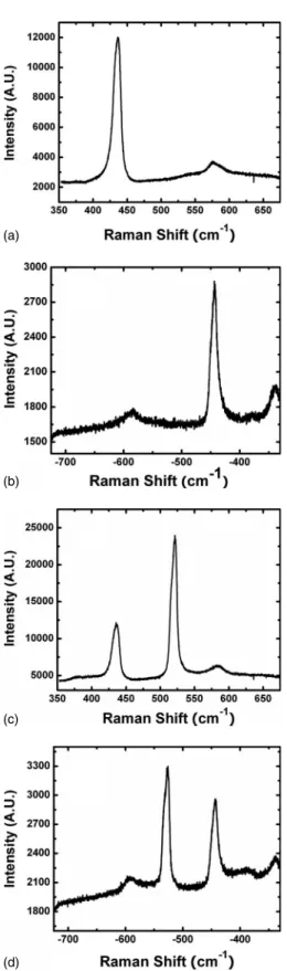
Figures5共a兲 and5共b兲 show the Stokes and anti-Stokes
Raman spectra of the ZnO bulk wafer, respectively, and Figs.
5共c兲and5共d兲 exhibit Stokes and anti-Stokes Raman spectra of the aligned ZnO nanorods, respectively. These spectra were collected to estimate the corresponding peak shift due to the local laser heating. Assuming that the laser heating of the bulk ZnO crystal is neglected关assuming that T=300 K in Eq. 共3兲兴, the temperature difference between the bulk ZnO and the aligned ZnO was found to be 2 ° C. The approxima-tion method used in the equaapproxima-tion can be justified since the temperature difference共⌬T兲 is significantly smaller than the square of the temperature共T2兲 in the denominator. The Ra-man peak shift due to the estimated temperature difference was calculated to be less than 0.2 cm−1. Therefore, the Ra-man peak shift due to the local laser heating can be ne-glected.
When the plasmon frequency p approaches the fre-quency of the LO phonon modeLO, the collective oscilla-tion of the free-electron gas begins to couple with the LO phonon via its associated longitudinal electric field. The LO phonon-plasmon coupled mode splits into two branches: High and lower frequency LPP modes are referred to as LPP+ and LPP− modes, respectively. Only the LPP+ mode can be detected if the plasmon is in the overdamped condi-tion, i.e., p⬍␥. The LPP+ mode in the Raman spectrum shifts to a higher frequency and an asymmetrical broadening occurs as the concentration of free electron increases. There-fore, the carrier concentration can be extracted by analyzing the Raman spectrum. The plasma frequency can be deter-mined by fitting the coupled A1共LO兲 plasmon-phonon peak using the following equation:
I共兲 = const · A共兲 · Im关− 共兲−1兴, 共4兲 whererepresents the relative Raman shift, 共兲 is the di-electric function, and A共兲 is the term that corresponds to the deformation potential and the electro-optic mechanism13and is expressed as follows: A共兲 = 1 + 2CTO 2 ␦ 关p2␥共TO2 −2兲 −2⌫共2+␥2−p2兲兴 + C2兵p2关␥共LO2 −TO2 兲 + ⌫共p2− 22兲兴 +2⌫共2+␥2兲其
冋
TO 4 ␦共LO 2 −TO2 兲册
, 共5兲 where ␦=p 2␥关共⌫兲2+共 TO 2 −2兲2兴 +2⌫共2+␥2兲共LO2 −TO2 兲, 共6兲 where C is the Faust–Henry coefficient, which can be de-duced from the ratio of the intensity of the LO to TO phonon modes in undoped ZnO using the following equation:26ILO ITO =
冉
l+LO l+TO冊
4 TO LO再
1 +TO 2 − LO 2 CTO2冎
, 共7兲where l is the frequency of the laser, p is the plasma frequency, and LO and TO are the LO and TO phonon frequencies for A1 mode, respectively.⌫ and␥ represent the phonon and plasmon damping constants, respectively. The
(b) (a)
(c)
(d)
FIG. 5.共a兲 Stokes and 共b兲 anti-Stokes Raman spectra of undoped ZnO bulk wafer.共c兲 Stokes and 共d兲 anti-Stokes spectra of aligned ZnO nanorods.
dielectric function共兲 in Eq.共4兲indicates the contributions from both phonon and plasmon:
共兲 = ⬁
冋
1 + ⍀ 2 TO 2 −2− i⌫− p 2 共+ i␥兲册
, 共8兲 where⍀2 is the simplification ofLO2−TO2 and⬁is the high-frequency optical dielectric constant. Equation 共4兲 can be fully expressed and simplified by substituting Eqs. 共5兲,
共6兲, and共8兲into it. The value ofp,␥, and⌫ can be obtained by fitting the experimental data with Eq. 共4兲. The carrier concentration can be determined from the plasmon frequency pby using the following expression:
p=
冑
4ne2⬁m*, 共9兲
where m* is the effective mass of the free carrier and is determined to be 0.23mefor ZnO.27 Finally, the mobility of the electron can be obtained from the plasmon damping con-stant␥ as follows:
␥= e
m*. 共10兲
TableIsummarizes the published ZnO Raman peak position for the various modes collected by other research groups. In this fitting, the wavenumbers of the TO and LO phonon modes were set to 378 and 574 cm−1, respectively, and the optical dielectric constant28and Faust–Henry constant29were set to 3.68 and 6.4, respectively.
The curve fitting results for the bulk ZnO and the aligned ZnO nanorods are shown in Fig.6共a兲. The line shape analysis of the bulk ZnO reveals a relatively low carrier concentration of 1.9⫻1017cm−3. This result corresponds to the A
1 peak position and FWHM of the coupled mode, as shown in Fig.
6共a兲. The Raman peak position of the A1共LO兲 mode for the aligned ZnO nanorods is 585.2 cm−1 and the FWHM of this peak is 22.9 cm−1. The fitting parameters and results are summarized in Table II. The carrier concentration and mo-bility of the bulk ZnO determined from the line shape analy-sis are 1.9⫻1017cm−3and 108.9 cm2/V s, respectively. The carrier concentration and mobility of the aligned ZnO nano-rods obtained from the line shape analysis are 3.8 ⫻1017cm−3and 84.8 cm2/V s, respectively. The mobility of the aligned ZnO nanorods is about 20% lower than that of
the undoped bulk ZnO, which can be attributed to the en-hanced surface scattering. Motayed et al.30studied this phe-nomenon using electron backscattered diffraction and sug-gested that the low mobility of the nanowire with intermediate diameter 共120–180 nm兲 might be related to grain boundary scattering. The experimental curve fitting re-sults were further studied by theoretical line shape analysis of the LPP mode as a function of the plasma frequency关Fig.
6共b兲兴. The peak of the A1共LO兲 reached its lowest limitation of 574 cm−1 while
p is 50 cm−1, which corresponds to the concentration of 2⫻1016 cm−3. The LPP mode line starts to TABLE I. Comprehensive summary of the frequency of the ZnO Raman phonon modes共in cm−1兲 reported by other research groups.
E2 low E2 high A1共TO兲 Quasi-A1共TO兲 E1共TO兲 Quasi-E1共TO兲 A1共LO兲 Quasi-A1共LO兲 E1共LO兲 Quasi-E1共LO兲 Ref. 101 444 380 395 398 413 579 585 591 585 13 102 439 379 ¯ 410 ¯ 574 ¯ 591 ¯ 32 ¯ 436 ¯ ¯ ¯ ¯ 582 ¯ ¯ ¯ 23 102 438 380 ¯ 409 ¯ ¯ ¯ 587 ¯ 33 102 437 379 ¯ 410 ¯ ¯ ¯ 591 ¯ 24 101 437 380 ¯ 407 ¯ 574 ¯ 583 ¯ 34 ¯ 441 381 ¯ 407 ¯ ¯ ¯ 583 ¯ 35 98 437.5 378 ¯ 409.5 ¯ 576 ¯ 588 ¯ 21 ¯ 436 383 ¯ ¯ ¯ ¯ ¯ 584 ¯ 36 ¯ 437 380 ¯ ¯ ¯ 583 ¯ ¯ ¯ 37 (b) (a)
FIG. 6.共Color online兲 共a兲 The LPP curve fitting results for the undoped bulk ZnO and the aligned ZnO nanorods.共b兲 Theoretical line shape of the LPP modes as a function of plasma frequency.
shift to a higher frequency and asymmetrical line shape broadening occurs whenpis larger than about 100 cm−1, as shown in Fig.6共b兲. The theoretically simulated curves as a function of different plasma frequencies showed an excellent agreement with the experimental data. Furthermore, capacitance-voltage共C-V兲 measurement of the undoped bulk ZnO was also performed to compare the carrier concentra-tion results obtained from both Raman scattering and C-V electrical measurement methods. The carrier concentration of the undoped bulk ZnO was in the range of 共1.3–2.5兲 ⫻1017cm−3, which confirmed that the LPP fitting result is fairly reliable.
Recent studies by Snure and Tiwari31 showed that the electrical resistivity of the ZnO film can be significantly re-duced by adding Ga dopant into the film. It might be an interesting topic for future work to study the electrical char-acteristics of Ga-doped ZnO nanorods.
SUMMARY AND CONCLUSIONS
The electronic properties of undoped bulk ZnO and well-aligned ZnO nanorods have been investigated using micro-Raman spectroscopy. It was found by micro-Raman spectroscopy that the ZnO nanorods are stress-free. The carrier mobility as well as the carrier concentration of undoped bulk ZnO and the aligned ZnO nanorods were determined by the line shape analysis of the A1共LO兲 phonon-plasmon coupled mode. The local laser heating effect was considered using the ratio of the E2mode Stokes to anti-Stokes Raman peak intensity. It is important to carefully consider laser heating effect when de-termining the frequency of the uncoupled LO phonon mode before performing the line shape analysis since the LO pho-non peak position depends on both the temperature and the LO phonon-plasmon coupling. The mobility and carrier con-centration of the undoped bulk ZnO obtained from the line shape analysis are 108.9 cm2/V s and 1.9⫻1017cm−3, re-spectively. The mobility and carrier concentration of aligned ZnO nanorods obtained from the line shape analysis are 84.8 cm2/V s and 3.8⫻1017cm−3, respectively. The C-V measurement of undoped bulk ZnO carrier concentration also further confirmed the carrier concentration obtained from LPP mode line shape analysis. The mobility of the aligned ZnO nanorods is about 20% lower than that of un-doped bulk ZnO, which can be attributed to the enhanced surface scattering due to the low dimension of the nanorod structure.
ACKNOWLEDGMENTS
The authors would like to thank Dr. Lynnette D. Madsen at National Science Foundation 共NSF兲 for funding this project. The project was supported by NSF under Contract No. DMR-0605270. The authors would also like to thank Dr. Bryan Chin. This research was partially supported by the USDA-CSREES under Grant No. 2006-34394-16953.
1Z. L. Wang,J. Phys.: Condens. Matter16, R829共2004兲.
2X. Duan, Y. Huang, Y. Cui, J. Wang, and C. M. Lieber,Nature共London兲
409, 66共2001兲.
3M. Law, D. J. Sirbuly, J. C. Johnston, J. Goldberger, R. J. Saykally, and P.
Yang,Science292, 1897共2001兲.
4A.-J. Cheng, Y. Tzeng, Y. Zhou, M. Park, T.-H. Wu, C. Shannon, D.
Wang, and W. Lee,Appl. Phys. Lett.92, 092113共2008兲.
5P. Zu, Z. K. Tang, P. Yu, G. K. L. Wong, M. Kawasaki, A. Ohtomo, H.
Koinuma, and Y. Segawa,Solid State Commun.103, 459共1997兲.
6D. M. Bagnall, Y. F. Chen, Z. Q. Zhu, T. Yao, S. Koyama, M. Y. Shen, and
T. Goto,Appl. Phys. Lett.70, 2230共1997兲.
7H.-M. Cheng, H.-C. Hsu, Y.-K. Tzeng, L.-J. Lin, and W.-F. Hsieh,J. Phys.
Chem. B109, 8749共2005兲.
8A. Tsukazaki, A. Ohtomo, and M. Kawasaki,Appl. Phys. Lett.88, 152106
共2006兲.
9J.-J. Wu and D. K.-P. Wong, Adv. Mater.共Weinheim, Ger.兲 19, 2015
共2007兲.
10A. F. J. Levi, J. R. Hayes, P. M. Platzman, and W. Wiegmann,Phys. Rev.
Lett.55, 2071共1985兲.
11C. L. Petersen and S. A. Lyon,Phys. Rev. Lett.65, 760共1990兲. 12S. Das Sarma, J. K. Jain, and R. Jalabert,Phys. Rev. B18, 6890共1978兲. 13H. Sato and Y. Hori,Phys. Rev. B36, 6033共1987兲.
14M. Giltrow, A. Kozorezov, M. Sahraoui-Tahar, J. K. Wigmore, J. H.
Davies, C. R. Stanley, B. Vogel, and C. D. W. Wilkinson,Phys. Rev. Lett. 75, 1827共1995兲.
15A. Mooradian and G. B. Wright,Phys. Rev. Lett.16, 999共1966兲. 16M. Park, J. J. Cuomo, B. J. Rodriguez, W.-C. Yang, R. J. Nemanich, and
O. Ambacher,J. Appl. Phys.93, 9542共2003兲.
17D. Wang, C.-C. Tin, J. R. Williams, M. Park, Y. S. Park, C. M. Park, T. W.
Kang, and W.-C. Yang,Appl. Phys. Lett.87, 242105共2005兲.
18A. B. Djurisic, W. C. H. Choy, V. A. L. Roy, Y. H. Leung, C. Y. Kwong,
K. W. Cheah, T. K. Gundu Rao, W. K. Chan, H. F. Lui, and C. Suryu,Adv. Funct. Mater.14, 856共2004兲.
19D. Wang, H. W. Seo, C.-C. Tin, M. J. Bozack, J. R. Williams, M. Park, N.
Sathitsuksanoh, A.-J. Cheng, and Y. Tzeng, J. Appl. Phys.99, 113509
共2006兲.
20K. Vanheusden, W. L. Warren, C. H. Seager, D. R. Tallant, J. A. Voigt, and
B. E. Gnade,J. Appl. Phys.79, 7983共1996兲.
21A. van Dijken, E. A. Meulenkamp, D. Vanmaekelberg, and A. Meijerink,
J. Phys. Chem. B104, 1715共2000兲.
22C. A. Arguello, D. L. Rousseau, and S. P. S. Porto,Phys. Rev.181, 1351
共1969兲.
23K. A. Alim, V. A. Fonobeov, and A. A. Balndin,Appl. Phys. Lett.86,
053103共2005兲.
24M. Balkanski, R. F. Wallis, and E. Haro,Phys. Rev. B28, 1928共1983兲. 25H. Fujimori, M. Kakihana, K. Loku, S. Goto, and M. Yoshimura,Appl.
Phys. Lett.79, 937共2001兲.
26W. L. Faust and C. H. Henry,Phys. Rev. Lett.17, 1265共1966兲. 27M. Oshikiri, Y. Imanaka, F. Aryasetiawan, and G. Kido,Physica B298,
472共2001兲.
28H. Yoshikawa and S. Adachi,Jpn. J. Appl. Phys., Part 136, 6237共1997兲. 29B. H. Bairamov, A. Heinrich, G. Irmer, V. V. Toporov, and E. Ziegler,
TABLE II. The fitting parameters and results of undoped bulk ZnO and aligned ZnO nanorods. A1共LO兲 peak position 共cm−1兲 A1共LO兲 FWHM 共cm−1兲 p 共cm−1兲 共cm⌫−1兲 ␥ 共cm−1兲 ne 共⫻1017cm−3兲 共cm2/V s兲 Bulk ZnO 575.5 12.6 153.7 63.0 427.0 1.9 108.9 ZnO nanorods 585.2 22.9 212.2 8.2 548.2 3.8 84.8
Phys. Status Solidi B119, 227共1983兲.
30A. Motayed, M. Vaudin, A. V. Davydov, J. Melngailis, M. He, and S. N.
Mohammad,Appl. Phys. Lett.90, 043104共2007兲.
31M. Snure and A. Tiwari,J. Appl. Phys.101, 124912共2007兲.
32K. A. Alim, V. A. Fonoberov, M. Shamsa, and A. A. Balandin,J. Appl.
Phys.97, 124313共2005兲.
33N. Ashkenov, B. N. Mbenkum, C. Bundesmann, V. Riede, M. Lorenz, D.
Spemann, E. M. Kaidashev, A. Kasic, M. Schubert, M. Grundmann, G. Wagner, H. Neumann, V. Darakchieva, H. Arwin, and B. Monemar, J.
Appl. Phys.93, 126共2003兲.
34T. C. Damen, S. P. S. Porto, and B. Tell,Phys. Rev.142, 570共1966兲. 35R. H. Callender, S. S. Sussman, M. Selders, and R. K. Chang,Phys. Rev.
B7, 3788共1973兲.
36L. Liao, D. H. Liu, J. C. Li, C. Liu, Q. Fu, and M. S. Ye,Appl. Surf. Sci.
240, 175共2005兲.
37G. W. Cong, H. Y. Wei, P. F. Zhang, W. Q. Peng, J. J. Wu, X. L. Liu, C. M.
Jiao, W. G. Hu, Q. S. Zhu, and Z. G. Wang,Appl. Phys. Lett.87, 231903