China 1991 International Conference on Circuits and Systems, June 1991, Shenzhen, China
A Concur rent Error- Detectable Module Design
for FFT Processing
Liang-Gee Chen and Thou-Ho Chen
Department of Electrical Engineering, National Taiwan University Taipei, Taiwan 10764, R . 0. C.
A B S ' I ' K A C ' I '
Most data in digital signal processing belong to the complex number system. Some characteristics of complex number computations can be utilized to reduce hardware overhead for concurrent error detection (CED) scheme. This paper presents a novel design of CED technique based on realization of direct complex computation approach. It is a time-redundant method, and the recomputation step is performed through exchanging strategy on both the real part and imaginary part circuits in a complex function. The hardware overhead then can be eliminated and the capability of error detection is still robust as duplicated module technique. Since pipelined processing can be
introduced to kill the recomputation cycle, the fast Fourier transform (FFT) processor based on pipelined butterfly module with the proposed CED technique is able to achieve real-time fault diagnosis. This technique can be applied to other complex number computing systems, and is more attractive especially in high-speed and high-reliability system.
I.
Introduction
To achieve high performance of digital signal processing (DSP), a task should be carried out through the use of massive processing elements by utilizing VLSI technology. Due to the increasing complexity and density of VLSI circuit, any failure of the chip may seriously damage all the operations of the system and hence high reliability will be more important requirement for future DSP system design. Concurrent error detection (CED) can detect errors during normal operation, many techniques by using either space redundancy, time redundancy or hybrid redundancy have been presented before[l]-[3]. They may need lower cost for achieving fault tolerance by means of using further steps of fault location and error correction. When those methods are used in DSP
computations, there is no need of knowing the data type, real or complex number. Unfortunately, since most data of DSP belong to complex number type, some merits which utilize characteristics of these complex number computations to advance the error detection capability are usually ignored.
In the recent research [4], it has been shown that the realization of direct complex computation with complex binary digits has lower circuit complexity than the implementation based on the conventional analytical computation through real number operators. In cooperating with the advance of VLSI technology, the realization through direct complex computation approach may become more and more attractive for special purpose future design of complex computing systems. Now consider that the error-detectable architecture in complex computing systems is to be constructed with the direct realization. In previous CED techniques, all operators, in real part and/or imaginary part, should be modified by the time-redundant scheme, space-redundant scheme or hybrid-redundant scheme to accomplish the concurrent error detection. With these concepts, this paper proposes a time-redundant scheme to directly utilize the complex computational units. It uses the exchanging strategy for both real and imaginary circuits within a complex function during recomputation to do error detection. This will result in almost no hardware overhead. Furthermore, pipelined processing can be introduced to kill the recomputation cycle. It is clear that this design is the best of all time-redundancy CED schemes when direct hardware-based implementation is considered.
The fast Fourier transform (FFT) process has played an important role in digital signal processing system. Typically, this transformation is performed as a pre-process of general DSP processing. Lately, three algorithm-level fault diagnosis methods [5]-[7] have been presented. Choi and Malek [SI proposed a CED technique, called recomputing by alternate path, to detect errors during normal operation. And it achieves fault tolerance by introducing a redundant stage. Jou and Abraham [6] described two algorithm-based techniques JAH and JAT, the former is to append the decoding multiplier stage and the latter recompute with modified input data one cycle after the normal computation has been executed, to provide fault detection. In [7], it used the combination of predicted sum coding stage and a simple CED to detect all of errors. However, there are several drawbacks: it cannot detect error until a full FFT processing latency; it has large latency of fault location; a half throughput reduction; slightly higher hardware overhead; and it may have effect of roundoff errors.
For overcoming above constraints, we propose an efficient and novel butterfly-level fault diagnosis method for a special purpose prkessor in real-time processing or where speed is of importance. This study is based on the principles of time redundancy and the natural feature of butterfly computation which includes complex addition and multiplication. A scheme that both the real part and imaginary part circuits are exchanged in recomputation has been employed to achieve concurrent error detection on butterfly operation. This design can detect errors concurrently with almost no extra hardware and the detecting capability is similar to that of duplicated module technique. A novel pipelined butterfly structure is furtherly developed to overcome the throughput degration due to the nature of time-redundant system.
Detection
11. The Scheme of Concurrent Error
Since the effects of faults within higher functional modules in VLSI can be described with accurate and tractable models. For simplicity, the discussion of fault model is based onabstraction level (or functional level). It means that our emphasis is on the verification of the functional behavior regardless of the precise nature of failure in a functional block. This assumption is reasonable because the major requirement of most CED techniques is to verify whether each processing element is functional.
This paper introduces a new time-redundant CED scheme, as shown in Fig. 1, in complex computing systems that during recomputation it uses exchanging computation of real and imaginary circuits within a complex function. There are two necessary conditions for implementing this scheme.
[Condition
I]
The complex function must have theindependence property which means that the real part circuit and the imaginary part circuit are independently operative. For the purpose of fault detection, operations of a good part circuit can not be interfered by another faulty part circuit. This indicates a satisfication on the principle of disjoint error sets.
[Condition 21 The real part circuit and the imaginary part
circuit should be or be modified as identical.
This will satisfy the principle of mappable correct output. With these two necessary conditions, it is reasonable that in a complex function any fault occurring in either the real circuit or the imaginary circuit can be detected. The same as duplicated module technique, both faulty part circuits may be unallowable.
m p l u fundional unil f
I
.)M t c s :
:rcrldrudt
(I)
:inUgiruryaradtw kboth real circuit and imaginary k u i l BIC modified BS identical
Fig. 1 The CED scheme of exchanging strategy in a complex functional unit f
Firstly, let f ( x R , X I ) and f ( X I , X R ) represent primary
computation and recomputation respectively, where f is a complex function and X R denotes data input to the real part
circuit and X I data input to the imaginary part circuit. And these two computations are performed within the same complex functional 'unit f . f ( X l , X R ) indicates that the real and
imaginary parts of data in primary computation are exchanged for input during recomputation. For accomplishing error detection, the original function's structure must be modified so that both real circuit and imaginary circuit are identical. Owing to independent operations of both real and imaginary circuits within f, a mismatch, ~ ( X R ,
4)
# f ( X I ,X,)
between these two results of computations implies a fault existed in this functional unit. Theoretically, the detecting capability is thesame as duplicated module technique.
Obviously, most complex computing functions can be decomposed into the basic complex addition, subtraction and multiplication. For complex addition/subtraction, its architecture will satisfy those two necessary conditions mentioned above and don't require modifications for equalizing both real and imaginary circuits. The following example of addition will give more understanding.
At first, consider the complex number X = X ,
+
j X I , X Rdenotes real part and X I imaginary part, the two's complement
representations using complex binary digit are
n - 2 i= 0 n - 2 i= 0
x ,
= - X,n.12n-l+
CXRi2i X I =-
XIn.12n-l+
C X l i 2 i n-2 i=Owhere xi = x R ~
+
jx,, and x R ~ , xli E (0, 1 ).
The computation of a complex full adder (CFA) is described as x i+
y i+
ci = ( x R ~+
y ~ i + cRi)+
j (xli+
y!i+
c ~ i ) and the functional diagram is shown in Fig. 2(a). Fig. 2(b) shows error detection scheme of the complex ripple carry adder. The fault model accepted by this design covers temporary faults and permanent faults as broadly. Typically, a faulty CFA which can be caused by FA fault and connection line fault mayaffect its output sum and carry-out. Our fault assumption is at most one failed FA within each CFA. This is an inherent problem of duplicated module method and is reasonably allowable. Apparently, the error detection capability of the proposed technique is the same as that of duplicated module technique, but without extra hardware redundancy. In addition, if there is only one faulty CFA, an active error signal ei which
comes from the least significant erroneous output bit will indicate that there are two potential faulty CFAs located in bit-slice i
-
1 and bit-slice i. And this can lead to the solution of faulty CFA location problem. For the same deduction, this CED scheme also can be applied to other FA-based adders, carry-select adder, carry-lookahead adder and the corresponding subtractors.But for multiplication, consider the product of two complex numbers X and Y , and it can be written as
x
= - x n.1 2"-1 + CXi2' ~ 840 ... ... ... f . : &6n-1
...s, ii
"1 61 %I$0 f : s R n . l s L - l ... S R I SI, ... 8 1 1 I1 SRO IO ... ... ei e en.lFig. 2 (a) Complex full adder (CFA)
(b) The CED scheme of the complex ripple-carry adder Based on direct complex computing approach, it is clear that in the above the subtraction in real part circuit and the addition in imaginary part circuit show both circuimes to be unequal. Although, subtraction and addition can be combined as unique addedsubtractor architecture, and will be implemented in both real and imaginary circuits in order to satisfy the necessary condition 2. To achieve independence of the necessary condition 1, two real multipliers and an adder/subtractor are required for the real part circuit, and also for the imaginary part circuit too. Thus, the exchanging computation strategy for both real and imaginary circuits also can be applied to the complex multiplication as complex addition described previously. The practical design will be carried out in fault-tolerant
FFT
processor, section
In.
From the error detection scheme mentioned above, it demonstrates that the proposed technique needs less extra hardware than other CED methods, only comparators and switching circuits are needed. For designing high-reliability complex computing system, the CED-based complex addition/subtraction and multiplication can be utilized to construct most functions in order to achieve fault tolerance.
111.
The Design
of
Fault-Tolerant FFT
Processor
The algorithm is complicated and the complex operation involved furtherly complicate their realization on a single chip. So far, the FFT process is always performed through microprogramming on a programmable chip, in which there is the least hardware required. However, in the case of applications in real-time or high-speed processing and with the advance of VLSI technique, we can implement those complex operations of butterfly module in the special purpose
FFT
processor directly with multipliers and adders. That is, each module will realize a parallel buttefly computation.
Since the proposed CED technique is a time-redundancy scheme, the throughput of the system will be reduced largely. To overcome this problem, a pipeline scheme is introduced into butterfly module. Though multistage pipelining is allowable, extra hardware and clock distribution problem will increase with the number of stages. Especially when the hardware cost of each stage is not much larger than pipeline registers, multistage is unworthy. Taking a better trade-off, we use two-stage pipelining to eliminate the extra recomputation cycle in the time-redundancy scheme.
At first, we decompose the butterfly computation into one complex addition, subtraction and one complex multiplication, as illustrated in Fig. 3. These complex operations are expanded as follows bw = (bR
+
Jbl)(WR+
J W I ) = (bRwR - blwl) + J(bRwl+ blwR) = (bw)R + j(bw), a 4- bw = (UR+
(bRWR - blwl))+
J(a,+ (bRW1+
blWR)) a-
bw = (OR - ( b R W R-
b1wl))+
J(a1- (bRW1-k b1WR)) Clearly, bw is the common product, and the realization needs four real multipliers and two real adder/subtractors. In addition, two real adders and two real subtractors are required to realize a+
bw and a - bw parallelly. (clmk cycle) CP Tbut (Sage 1) (stage 2) a + bw b a - bwCED butterfly module
(a-bw), (a-bwh (a-bw), (a-bw), (a-bw),
1
1
1
1
1
1
1
1
1
1
0 1 2 3 4 5 6 1 8 9 1 0 1 1;
W Cl c2 Fig. 3 Two-stage pipelined diagram in a butterfly modulen
n
n
n
n
n
n
n
n
n
Assume that the operation time of a butterfly module is TbW It can be written as Tbut = Ta+bw = A multiplication cycle is denoted as Tmul. Fig. 3 shows the two-stage pipeline diagram in a butterfly module where stage 1 performs the common product bw and stage 2 performs addition and
subtraction of a and bw, and in which there is TbU = T I
+
T2where T , > T2. In the proposed design, each stage must be
checked respectively. Since time delay of multiplication in stage 1 is larger than addition's in stage 2. Hence the latency of stage 1 needs to be reduced as equal about to that of stage 2 as possible for obtaining better pipelining. Considering implementation of bw, two multipliers and one addedsubtractor are needed to realize (bwjR, the real part of bw, and the same for imaginary part. Using Baugh-Wooley two's complement multiplier [8], a ripple-carry adder/subtractor can be merged into the two multipliers such that we can efficiently obtain T I =
Tmr = Tmul where TmUr denotes the computing time of this
combined multiplier-adder structure. In order to derive a better performance in stage 1, another two substages pipeline is introduced into the combined structure for eliminating recomputation cycle during which exchanging computation of real and imaginary circuits is executed for achieving error detection.
Due to two-substage pipeline and time-redundancy CED scheme used in stage 1, the throughput latency is about equal to
the computing time, (2n
+
l)rFA whererFA
denotes the time delay of a full adder, of the combined multiplier-adder as inn-bit system. For satisfying the pipeline principle, the throughput latencies, including CED scheme, of stage 1 and stage 2 should be identical. Then the adders and subtractors in stage 2 are constructed with ripple-carry design. This is because the computing time of the ripple-carry adder or subtractor in n-bit system is equal to ntFA. With the exchanging strategy CED scheme proposed, the throughput latency is nearly equal to that of stage 1. Besides, when using adders or subtractors with half of (2n
+
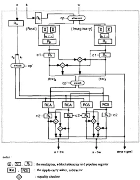
l)rFA, the ripple-carry design needs less hardware and hence it can reduce the total hardware cost. Fig. 4 shows the schematic diagram of concurrent error detection in pipelined butterfly structure. The timing diagram is described in Fig. 5 under original and pipelined with CED butterfly operation. From these results, it has been shown that the throughput latency of an error-detectable butterfly computation is about equal to time delay of a real array multiplier. As soon as the faulty butterfly module is identified, reconfigurations with spare allocation can be applied to FFTnetwork to achieve fault tolerance.
l b
Fig. 4 The schematic diagram of the pipelined butterfly structure with CED scheme
Pipelined:
nok in L e above. u c h cycle denma (n + l)lFA where iFA is l m c &lay of a full adder
0
: emor checkingFig. 5 The timing diagram under the original/pipelined with CED butterfly operation
The comparison of four schemes, JAH [6], THCH [7], CMT [5] and the proposed scheme which is referred to as the CCT, of fault-tolerant
FFT
processor is shown in Table I. For achieving concurrent error detection, by utilizing exchanging strategy for both real and imaginary circuits, the hardware overhead is only for comparators and switches. Utilizing the data of CMOS technology, the total hardware overhead is aboutl l ( n + 4 ) where n denotes word length. Since the proposed diagnosis scheme is based on butterfly-level, error can be
detected during each butterfly operation without waiting for full
FFT
processing latency in other schemes which are based on algorithm-level. By using pipelined scheme in each butterfly module, the error detection latency is reduced to half of a butterfly operation cycle, less than other previous methods. No additional error location processing or error retry algorithm are required, and the diagnosis latency is only one cycle, a butterfly operation time. There is no effect of roundoff errors existed in our system. In particular, only one faulty butterfly-module can be diagnosed for JAH and CMT, but CCT has no limit in diagnosis capacity. If realization of direct complex computations is possible, the CCT scheme will be much more attractive than other time-redundant schemes.IV.
Conclusions
A novel CED-technique which uses realization of direct complex computation approach with exchanging strategy in both real and imaginary circuits is proposed. This technique belongs to time-redundant system and needs very little hardware overhead. The detecting capability is robust as the duplicated module technique. When cooperated with pipelined butterfly structure of
FFT,
the recomputation delay problem canbe overcome as to normal operation. Because of only requiring negligibly additional checking time, the nearly real-time diagnosis is achieved. From the experimental results, it can be shown that the proposed technique will be very suitable for designing high-speed and high-reliability DSP/VLSI system.
~~~~ ~ ~ ~ ~ ~
unknown (log2 N) + 5
-
0Diagnosis latency (cycles) 2
Diagnosis capacity 1 1 1 no l i t
(No. of faulty butterflys)
R e f e r e n c e s
[ 11 B.W. Johnson, Design and analysis of foult tolerant digital systems, Addison-Weesley, 1989.
[2] J.H. Pate1 and L.Y. Fung, "Concurrent error detection in ALUs by recomputing with shifted operands," IEEE Trans. Computers, C-31, pp. 589-595, July 1982,
131 L.G. Chen and T.H. Chen, "Computation with simultaneously concurrent error detection using bi-directional operands," Proc.
IEEE
ICCD, 1989, pp. [4]K.Z.
Pekmesstzi, "Complex number multiplier," IEE Proc.E , Comput. & Digital Tech., vol. 136, pp. 70-75, Jan.
1989.
[ 5 ] Y.H. Choi and M. Malek, "A fault-tolerant FFT
Drwessor." IEEE Trans. Computers, C-37, pp. 617-621, 128- 13 1.
..
May 1988.
[6] J.Y. Jou and J.A. Abraham, "Fault-tolerant FFT networks," IEEE Trans. Computers, C-37, pp. _ . 548-561, May 1988.
[7] D.L. Tao, C.R.P. Hartmann and Y.S. Chen, "A novel concurrent error detection scheme for FFT networks,"
20th IEEE Fault-Tolerant Computing Symposium, 1990,
[8] K. Hwang, Computer arithmetic-principfes, architecture
ana' design, Wiley, New York, 1979.
pp. 114-121.
TABLE I
Comparison Of Fault-Tolerance Schemes For N-point FFT Processor
note : in the above, a cycle means a full butterfly operation time, n the word length and N the number of
FFT
points.#: the proposed method.
# I : regardless of switches and comparators.
# # U : including switches and comparators, and using CMOS technology