Effect of crystal orientation and doping on the activation energy
for GaAs oxide growth by liquid phase method
Hwei-Heng Wang, Dei-Wei Chou, Jau-Yi Wu, Yeong-Her Wang,a)and Mau-Phon Houng Department of Electrical Engineering, National Cheng-Kung University, Tainan, Taiwan,
Republic of China
共Received 2 September 1999; accepted for publication 13 October 1999兲
We have investigated the oxide growth kinetics of near-room-temperature liquid phase chemical enhanced oxidation on differently oriented and doped GaAs substrates. Oxidation reactions have been studied by analyzing their activation energies and have been found to depend on the bond configuration of crystal planes. Experimental results indicate that the activation energies are independent of the doping of GaAs. The oxidation rates are dopant selective (n⫺: p⫹-GaAs⬃4:1 at 30 °C under illumination兲 and sensitive to illumination 共without:with illumination⬃1:25 at 30 °C for a n⫹-doped GaAs兲. In the oxidation reactions, photogenerated holes are found to play an important role. Finally, we have proposed a mechanism based on the band bending and the carrier transport near the oxide-GaAs interface to interpret the experimental observations. © 2000 American Institute of Physics. 关S0021-8979共00兲04002-0兴
I. INTRODUCTION
Liquid phase chemical enhanced oxidation 共LPCEO兲 method has been successfully utilized for producing an insu-lating oxide layer on GaAs substrates efficiently (⬃1000 Å/h at 70 °C兲 under relatively low temperatures (30– 70 °C兲.1As for device applications, we have also successfully demon-strated a GaAs metal–oxide–semiconductor field effect tran-sistor with a LPCEO gate oxide.2Comparing with other oxi-dation techniques such as thermal, anodic, or plasma oxidation of GaAs, the LPCEO technique has many advan-tages upon them. For example, unstoichiometry共partial loss of As oxides兲 due to significant difference of vapor pressure between Ga and As compounds at high temperatures can be avoided. In addition, the oxidation rate is fairly high at such low temperatures, as compared with the case of thermal oxi-dation (⬃50 Å/h at 450 °C兲.3 Hence, it is convenient and reliable to use a photoresist mask to achieve selective-area oxidation by the LPCEO technique.4 Neither electric poten-tial nor assisted energy source共plasma or photo兲 is applied in the LPCEO technique. As compared with extensive research
efforts such as high-pressure5 or photoenhanced
techniques,6–8 the LPCEO method is quite simple and eco-nomic.
To date, the exact mechanism of GaAs oxidation is still not very clear. Most models of GaAs oxidation were built for thermal or anodic oxides.9,10Because no electric potential is applied and the oxidation temperatures are relatively low, we expect that the mechanism of LPCEO is different from those of thermal and anodic oxidation. For such an ‘‘electroless’’ oxidation process under low temperatures, a clear mecha-nism about the dependence of the orientation or doping on the oxidation of GaAs has not been elucidated yet. In this article, some experimental results of the crystal orientation
and doping dependence on the GaAs oxide growth by the LPCEO technique will be reported. Since the oxidation con-ditions are quite different from those of the thermal and an-odic methods, some other points of view will be proposed to clarify the mechanism of LPCEO. The effects of GaAs sur-face structure, doping of the substrates, and also the light irradiation on the oxidation kinetics will be characterized by analyzing the activation energies (Ea) using Arrhenius plots.
II. EXPERIMENT
Experimental apparatus for the LPCEO technique is very simple and consists of a temperature regulator and a pH meter, as shown in Fig. 1. A more detail description about the technique can be found in Ref. 1. For an optimum oxi-dation condition, a range of initial pH values 4⬍pHi⬍4.5
was set in the following experiments. One-side polished and epiready GaAs wafers grown by liquid encapsulated Czo-chralski 共LEC兲 technique with orientations of 共100兲, 共110兲, and 共111兲 were employed as specimens in the study of ori-entation effects. The roughness of these wafers are about 3 Å 共rms values兲 according to measurements by atomic force mi-croscopy. Doping of these wafers are all heavily Si doped at concentrations of 1 – 1.5⫻1018cm⫺3 (n⫹doped兲. To inves-tigate the doping effects on the oxide growth, we addition-ally employed other three doping types of the共100兲-oriented wafers. They are n⫹ wafers with ⬃1.5-m-thick epilayers doped at 2⫻1016 cm⫺3 (n⫺ doped兲, Zn doped at 1.1– 1.4 ⫻1019cm⫺3( p⫹doped兲, and undoped 共with a resistivity of 4 – 9⫻107 ⍀ cm).
An As-terminated surface is less stable when exposing to air because of its electronic activity. In order to unify and stabilize the surfaces, these specimens were all immersed into a 10%–20% NH4OH solution for 1 min to produce a more stoichiometric and less contaminated surface with less excess As and a higher Ga/As ratio.11,12 Immediately, the
a兲Electronic mail: [email protected]
2629
specimens were then immersed into the oxidation solution under a constant temperature for 1 h, and the temperatures are 30, 50, and 70 °C, respectively. To study the effects of illumination on the oxide growth, we placed a 13 W fluores-cent lamp above the specimens with a distance of 15 cm. In the case of the oxidation without illumination, the lamp was turned off, and the specimens were turned around against the indoor light. The as-grown specimens were rinsed by de-ionized water and dried in nitrogen after oxidation.
III. RESULTS AND DISCUSSION A. Effects of crystal orientation
As illustrated in Fig. 2, a brief review of GaAs crystal planes is introduced. By looking down from the Ga-terminated 共111兲 plane 关共111兲Ga兴 plane, we can get one Ga atom connected by three covalent bonds to As atoms at the lower layer, leaving one outward bond. It is also possible to have one As atom connected by one bond to Ga with three outward bonds. The first situation is energetically favored and the second does not appear to even exist. Therefore, each atom at the共111兲 plane appears to be theoretically with one outward bond at the 共111兲 plane. However, some previous works suggested a structure with 1/4 Ga monolayer
vacan-cies in the layer at the Ga-terminated 共111兲 plane.13,14Once the vacancies exist, we believe that each atom at the plane will have more than one outward bond. It will be discussed later that the bond number at the共111兲 plane is evaluated to be about 1.7 based on the experimental results.
The共100兲 plane of GaAs consists of either all Ga or all As atoms. In either case, each atom is attached by two bonds to atoms in the lower layer, leaving two free outward bonds. Each atom has two outward bonds regardless of whether the plane is made up of Ga or of As atoms. At the共110兲 plane, in contrast, the atoms contain an equal density of Ga and As atoms. Each atom is attached by one bond to the lower-layer atom, two bonds to nearest neighbors at the plane, leaving only one outward bond. Therefore, it is the preferred cleav-age plane for GaAs because interatomic force is weak be-tween adjacent共110兲 planes.
An Arrhenius plot is obtained through plotting the loga-rithm of oxidation rates against the reciprocal of absolute temperatures, as shown in Fig. 3. The Arrhenius equation is
R⫽A exp
冉
⫺qEakT
冊
, 共1兲where R is the oxidation rate, Eais the activation energy, T is
the absolute temperature in K, A is the frequency factor, k is Boltzmann’s constant, and q is the electronic charge. Since a high oxidation rate arises from a high concentration of the reaction sites, the initial rate of thermal oxidation of crystal-line Si is directly proportional to atom density of the crystal planes.15 However, there are considerable differences in the results of GaAs oxidation by the LPCEO technique. The re-sults indicate that the slope of the straight line for the 共110兲-oriented GaAs is more negative than those of 共111兲 and 共100兲 oriented. A higher slope of the Arrhenius curve implies a higher Ea value (Ea⬃0.56 eV兲, which indicates that the oxidation is more difficult at the 共110兲 plane, although the atom density at this plane is higher than the other two planes. The Ea values for the 共100兲 and 共111兲 surfaces are much
lower (Ea⬃0.24 eV兲 and approximately equal to each other.
By the LPCEO method, the oxides grow at a relatively low temperature. Therefore, kinetic energies in the molecules are much lower. To react, chemically active atoms or bonds be-come predominant. In general, lower energies in the mol-ecule result in a lower rate of reaction, but somehow the FIG. 1. Experimental apparatus for the LPCEO technique in the present
work.
FIG. 2. A simplified schematic model illustrates a GaAs crystal along共110兲, (001¯ )Ga,共111兲Ga, and the (1¯1¯1¯)As planes. The single lines represent the bonds in the plane of the figure, whereas the double lines represent two bonds directed out of and into the plane. The dots indicate the outward 共available兲 bonds of each atom.
FIG. 3. Arrhenius plot for oxide films grown on 共100兲, 共111兲, and 共110兲-oriented GaAs by the LPCEO technique.
oxidation rate is abnormally high in the LPCEO technique. Thus, there may be some other factors as important as 共or more than兲 the atom density in the oxidation. A possible interpretation for the earlier experimental results is that the higher outward 共available兲 bond densities at the 共111兲 and 共100兲 plane results in lower values of the Ea, since the bonds
are considered to be more chemically active than neutral at-oms.
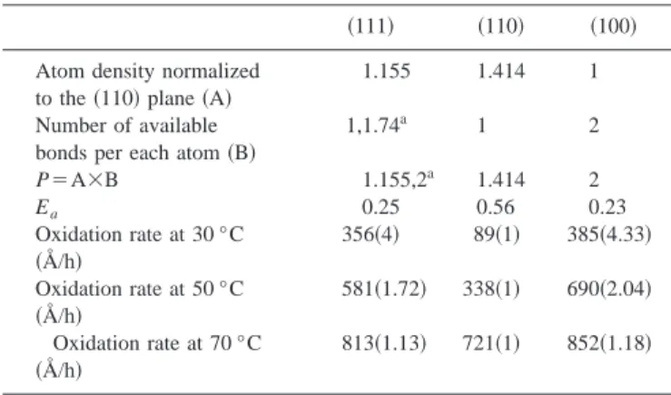
Table I summarizes the oxidation rates of these orienta-tions comparing with the corresponding configuraorienta-tions of the atom density normalized to the共100兲 plane 共A兲 and the num-ber of available bond per each atom共B兲, where P is defined as the product of them ( P⫽A⫻B) in the following investi-gations. The evaluated value of P for the共100兲 plane is two, and that for the共111兲 plane is 1.155 共in the case of each atom at the共111兲 plane has only one available bond兲. As discussed earlier, each atom at the共111兲 plane probably has more than one available bond because of the presence of Ga vacancies. According to the experimental evidence of that the activation energies and the oxidation rates of共100兲 and 共111兲 planes are nearly identical, the equivalent number of the available bond per each atom at the共111兲 plane is evaluated to be about 1.7 (1.155⫻1.7⯝2). Hence, this implies that there are approxi-mately 17 available bonds on ten atoms at the 共111兲 plane. On the other hand, the P value is 1.414 at the 共110兲 plane, which results in a relatively low oxidation rate as compared with the other two planes. Previously, an experimental result indicated that the 共110兲 surface exhibits an absolutely mini-mum of oxygen adsorption ability,16which is consistent with our observation.
B. Effects of doping
Figure 4 shows an Arrhenius plot for specimens of
共100兲-oriented GaAs with doping conditions of
n⫹, n⫺, p⫹, and undoped. The specimens were all oxi-dized under illumination. Unlike the results of the orientation effects, the values of Ea for these specimens are found to be
close to each other (⬃0.24 eV兲. As a result, the Ea is not
dominated by the doping of GaAs but by the crystal orienta-tion. On the other hand, the intercepts of the Arrhenius
curves with y axis for the n⫺- and n⫹-doped GaAs are found to be larger than those for the p⫹ and undoped. The larger intercept implies a higher oxidation rate 共frequency factor兲. The rate ratio between the n⫺-GaAs and the p⫹-GaAs is about 4:1 at 30 °C. As will be discussed later, the doping of GaAs influences the oxidation rate because of dopant-dependent band bending near the oxide-GaAs interface.
A model of photoelectrochemical etching of GaAs sug-gests that the etching requires holes to oxidize GaAs at the interface,17and then the oxidized species is dissolved by the etchant. The initial stages of GaAs oxidation can be de-scribed as the following equations:
0→e⫺⫹h⫹, 共2兲
GaAs⫹6h⫹→Ga共III兲⫹As共III兲. 共3兲
After the electron-hole pairs generate by absorption of light 关Eq. 共2兲兴, GaAs is oxidized by the holes 关Eq. 共3兲兴. In the LPCEO technique, the oxidized GaAs remain undissolved in the solution because of a pH-dependent solubility within a controlled pH range.18 As a result, thick oxide films can be grown in the solution. As will be discussed later, the light illumination takes a great influence on the oxide growth. Thus, we expect that holes are also required in the LPCEO reactions and they are photogenerated. According to Eq.共3兲, as the photogenerated holes are supplied at a higher rate, the rate of oxidation of GaAs will be elevated.
The band bending of the near-interface region takes a great influence on the hole transport, since a built-in electric field drives the holes away from the interface or in the op-posite direction. Extrinsic states at the junction which pin the Fermi level are induced, as the GaAs surface is attached by oxidizing molecules, metals, or some liquid electrolytes. As a result, the band bending of GaAs is relative to the Fermi level pinning at the oxide-GaAs or the electrolyte-GaAs het-erojunctions. In the case of surface adsorbed by oxygen, the pinning of Fermi level of a n-doped GaAs is about 0.8 eV below the conduction band minimum, whereas that of a p-GaAs is about 0.5 eV above the valance band maximum.19 Therefore, the near-interface bands bend up in the n-GaAs, whereas they bend down in the p-GaAs. At the same time, electric fields are built in the near-interface regions. As illus-trated in Fig. 5, the photogenerated holes in the p⫹-GaAs TABLE I. Summary of the surface bonding configurations of共111兲, 共110兲,
and共100兲 surfaces of a GaAs crystal. It also lists the oxidation rates of these surfaces at 30, 50, and 70 °C. Values in parentheses are the rate ratios normalized to those of the共100兲 surface.
共111兲 共110兲 共100兲
Atom density normalized 1.155 1.414 1
to the共110兲 plane 共A兲
Number of available 1,1.74a 1 2
bonds per each atom共B兲
P⫽A⫻B 1.155,2a 1.414 2 Ea 0.25 0.56 0.23 Oxidation rate at 30 °C 356共4兲 89共1兲 385共4.33兲 共Å/h兲 Oxidation rate at 50 °C 581共1.72兲 338共1兲 690共2.04兲 共Å/h兲 Oxidation rate at 70 °C 813共1.13兲 721共1兲 852共1.18兲 共Å/h兲 a
Values evaluated in this work.
FIG. 4. Arrhenius plot for oxide films grown on n⫺, n⫹, p⫹, and undoped GaAs by the LPCEO technique.
will be repelled from the interface by the built-in electric field. In contrast, the holes are attracted to the interface by the electric field in n⫹-doped GaAs. A higher oxidation rate for the n⫺-doped GaAs are obtained because more photoge-nerated holes are supplied from the wider depletion region as compared with the relatively thin depletion layer in the n⫹-GaAs.
Figure 6 shows an Arrhenius plot to illustrate the light illumination effects on the LPCEO oxide growth. For a n⫹-GaAs oxidized under light illumination, we have found that the oxidation rate is significantly elevated共solid circles with the continuous line兲, as compared with those without illumination共the dashed line兲. At 30 °C, the rate of oxidation with illumination is elevated to be 25 times higher than the unilluminated. The increase in the oxidation is due to that more holes are photogenerated and accumulated at the oxide-GaAs interface, as compared with a relatively low concen-tration of holes in an unilluminated n⫹-GaAs. In contrast, almost no elevation in the oxidation rate for a p⫹-GaAs is found for the specimens under illumination 共solid squares兲. As discussed earlier, this is because most of the photogener-ated holes are repelled by the electric field away from the interface. For an undoped GaAs oxidized without illumina-tion, lack of holes at the interface results in a relatively low oxidation rate, which is similar to the case of n⫹-GaAs.
Un-der illumination, the rate of oxidation also becomes higher; however, the increase is insignificant. The oxidation rate is elevated to be only comparable with that of the p⫹-GaAs, which implies that photogenerated holes in the undoped GaAs are also repelled. Therefore, the bands also bend down near the interface in the undoped GaAs. The interpretation is consistent with a mechanism that an undoped GaAs grown by the LEC technique has a residual p background.20 In ad-dition, we have observed that the Eavalues were reduced for
all doping specimens under illumination and the observation implies that the surface chemistry becomes more active.
IV. CONCLUSION
In conclusion, the effects of crystal orientations and dop-ing on the GaAs oxide grown by liquid phase chemical en-hanced oxidation technique have been investigated. It has been found that the activation energy for the 共110兲-oriented plane is higher than those of 共100兲 and 共111兲 planes. A pos-sible mechanism is proposed based on the relatively lower product of the normalized outward 共available兲 bond density at the共110兲 plane. Based on the earlier mechanism and the experimental results, the number of available bond per each atom at the共111兲 plane has been evaluated to be about 1.7. It
is also found that the holes photogenerated in
n⫹, n⫺-doped, or undoped GaAs result in a higher rate of oxidation. Without any repelling electric field in the near-interface region, the elevation in the oxidation rate by illu-mination is more significant. For p-GaAs, however, the ef-fects of illumination on the oxidation rate are insignificant due to the depletion of holes which are repelled by the band-bending-induced electric field.
ACKNOWLEDGMENTS
This work was supported in part by National Science Council under the Contract Nos. NSC 88-2215-E006-009 and NSC 89-2215-E006-006.
1H. H. Wang, C.J. Huang, Y. H. Wang, and M. P. Houng, Jpn. J. Appl.
Phys., Part 2 37, L67共1998兲.
2J. Y. Wu, H. H. Wang, Y. H. Wang, and M. P. Houng, IEEE Electron
Device Lett. 20, 18共1999兲.
3
S. P. Murarka, Appl. Phys. Lett. 26, 180共1975兲.
4H. H. Wang, Y. H. Wang, and M. P. Houng, Jpn. J. Appl. Phys., Part 2 37,
L988共1998兲.
5N. Basu and K. N. Bhat, J. Appl. Phys. 63, 5500共1988兲. 6
C. W. Wilmsen, P. D. Kirchner, J. M. Baker, D. T. McInturff, G. D. Pettit, and J. M. Wooldall, J. Vac. Sci. Technol. B 6, 1180共1988兲.
7Z. Liliental-Weber, C. W. Wilmsen, K. M. Geib, P. D. Kirchner, J. M.
Baker, and J. M. Woodall, J. Appl. Phys. 67, 1863共1990兲.
8P. A. Bertrand, J. Electrochem. Soc. 132, 973共1985兲. 9
C. W. Wilmsen, R. W. Kee, and K. M. Geib, J. Vac. Sci. Technol. 16, 1434共1979兲.
10C. W. Wilmsen, J. Vac. Sci. Technol. 19, 279共1981兲.
11S. Osakabe and S. Adachi, J. Electrochem. Soc. 144, 290共1997兲. 12
C. C. Chang, P. H. Citrin, and B. Schwartz, J. Vac. Sci. Technol. 14, 943 共1977兲.
13S. Y. Tong, G. Xu, and W. N. Mei, Phys. Rev. Lett. 52, 1693共1984兲. 14M. Alonso, F. Soria, and J. L. Sacedon, J. Vac. Sci. Technol. A 3, 1598
共1985兲.
15
B. E. Deal, J. Electrochem. Soc. 125, 576共1978兲.
16W. Ranke, Y. R. Xing, and G. D. Shen, J. Vac. Sci. Technol. 21, 426
共1982兲. FIG. 5. Diagrams of the energy bands near the oxide-GaAs interface during
oxidation.
FIG. 6. Arrhenius plot showing the light-illumination effects on the oxide growth by the LPCEO technique.
17R. Khare, D. B. Young, G. L. Snider, and E. L. Hu, Appl. Phys. Lett. 62,
1809共1993兲.
18H. H. Wang, J. Y. Wu, Y. H. Wang, and M. P. Houng, J. Electrochem.
Soc. 146, 2328共1999兲.
19W. E. Spicer, P. W. Chye, C. M. Garner, I. Lindau, and P. Pianetta, Surf.
Sci. 86, 763共1979兲.
20J. R. Oliver, R. D. Fairman, R. T. Chen, and P. W. Yu, Electron. Lett. 17,