國立臺灣大學高分子科學與工程學研究所 碩士論文
Institute of Polymer Science and Engineering College of Engineering
National Taiwan University Master Thesis
低溫處理與氧化鉿阻擋層
對於高分子太陽電池效率及穩定性之研究
Performance and Durability of Polymer Solar Cells by Low-Temperature Drying Process and
HfO
2Blocking Layer
林恩詠 En-Yung Lin
指導教授:蔡豐羽 博士 Advisor: Feng-Yu Tsai, Ph.D.
中華民國 98 年 12 月
December, 2009
致謝
首先感謝上帝,一路帶領我,給我一切美好的經歷和環境。
感謝老師在碩班期間的指導。在老師身上學到非常多正面的態度及思考邏輯,
雖然經歷很多的實驗上的不順利,但是老師還是很有耐心的帶領著,能夠在這麼 嚴謹卻又自由的環境學習真的非常幸福。感謝廖文彬教授及戴子安教授百忙之中 擔任我的口試委員,老師的建議與指導給我更多元的思考方向。
感謝我的師父-強哥,謝謝你把我從零教到有,很有耐心的教我最基礎的東 西,跟你一起討論研究的日子真的很難忘;感謝大師兄像盞明燈,總是給予最中 肯的建議和實驗上的幫助。從兩位學長身上學到不只實驗,還有態度。感謝君展 大大、嫩嫩還有至敏,在我剛進實驗室時給我的溫暖跟幫助,你們都是我的榜樣;
感謝愛鬥嘴可是阿莎力的傅榆,毫不猶豫的借我ALD 時段;感謝我的最佳戰友
俊廷,互相打氣跟鼓勵的日子真的很值得回憶。感謝三位學弟:最能幹的銘宏、
最可愛的嚴修和最貼心的哲誠,你們總是竭盡所能的幫忙我;感謝說話很有精神 的政宏、講話很小聲的貽能、很犀利中肯的小砲、最後半年出現的譽泰哥、國小 同學沅昱,小學弟培偉跟柏榆,有時候都要請你們作苦力辛苦了。實驗室的各位
就像我的兄弟姊妹一樣,這段期間非常的溫暖開心。謝謝XXman、鳥人、蔡燁、
摸兔、毛、佳穎等平時的打氣。感謝陳文章老師及實驗室的學長們,平時測量都 麻煩您們了。
最感謝我偉大的男友圭鈺,一路看我跌跌撞撞考進研究所,又跌跌撞撞的畢 業。開心的時候要陪我笑,難過的時候負責安慰及提振我士氣,去當兵了還要遠 距離關心我,完全感謝,我撐過來了。
感謝我的家人:每天為我禱告的爸爸、媽媽、奶奶、姐姐,還有新成員姐夫,
在我求學路上不知道被我嚇過多少次了。感謝你們給我平順的心情以及正面的力 量,我愛你們。
兩年半的碩班我獲得很多,感謝每一位大家。
i
摘要
高分子太陽能電池的效率以及劣化問題廣為被研究與改善。而本篇針對以聚 (3-己烷基噻吩)(P3HT)為電子施體和碳六十衍生物(PCBM)為電子受體的異質接 面(Bulk Heterojunction)高分子太陽能電池,分別利用改變製程以及元件結構來達 到效率的提升以及劣化的改善。
在本研究的第一部分(第二章),我們利用低溫製程來改善元件物理性的形態 劣化。相較於室溫乾燥過程,將高分子主動層在低溫的情況下乾燥成膜,可以增 加聚(3-己烷基噻吩)的成核行為。並且在經過 190 度的熱退火後,密集的聚(3-己 烷基噻吩)結晶提供更大的結晶度,並且阻擋碳六十衍生物的大規模聚集,使雙
成分有很好的分散性。此高結晶的主動層型態提供 4.3%的太陽能電池效率,同
時其聚(3-己烷基噻吩)和碳六十衍生物緊密的型態提供了更好的的熱穩定性,改 善了元件內因物理型態改變減少介面的劣化問題。
而本研究第二部分(第三章)專注於元件因不穩定的 ITO 導電玻璃和電洞傳輸 層(PEDOT)所造成的化學性劣化。電洞傳輸層(PEDOT)在吸收水氣之後會侵蝕 ITO 導電玻璃,釋放出銦離子。為了解決這樣的化學劣化,我們利用原子層沉積
成膜技術(ALD)所長的氧化鉿(HfO2)來做為阻擋層。我們使用兩種結構討論對原
件所帶來的影響:當我們將氧化鉿層嵌入電洞傳輸層中作為銦離子阻擋層,發現 經過長時間的儲存實驗,此種元件結構會帶來更嚴重的劣化;但若將氧化鉿沉積
在電動傳輸層與 ITO 導電玻璃間,卻可以降低原件的衰退,我們將此歸因於養
化鉿的保護阻擋了化學反應的發生,並且以X 光光電子能譜儀(XPS)的縱深分析
圖作為佐證。
因此,本研究所提出的製程及元件結構改良,皆可以成功的應用在異質介面 型太陽能電池,並且提升元件之壽命。
ii
Abstract
This study realizes improvements in the efficiency and stability of bulk-heterojunction polymer solar cells using two approaches: morphological manipulation of the active layer composed of poly(3-hexylthiophene) (P3HT) and [6,6]-phenyl C61 butyric acid methyl ester (PCBM), and elimination of the adverse effects caused by the out-diffusion of the indium tinoxide (ITO) anode.
In terms of morphological manipulation, we developed a low-temperature drying process for the active layer that achieved significantly higher power conversion efficiency (PCE) (4.3%) and longer device lifetime (> 1250 h) than those of the standard room-temperature process. The improvements were attributed to the enhanced nucleation of the P3HT crystallites and the restricted large-scale aggregation of the P3HT/PCBM phases at the low drying temperature, which produced a densely interconnected P3HT crystal network that maximized the bulk-heterojunction area and prevented the active layer from morphological shifts with use.
In terms of diffusion blocking, we demonstrated that an ultra-thin (0.9 nm) layer of HfO2 deposited by atomic layer deposition (ALD) on the ITO anode effectively eliminated the degradation caused by the out-diffusion of In ions from the anode,
iii
while it also improved the PCE of the solar cells. The effectiveness of the ALD HfO2
blocking layer was owing to the excellent surface coverage and low defect density of the ALD films, and the improvement in PCE was due to the raised electrical field by inserted HfO2.
iv
Contents
Acknowledgement ... i
Abstract (Chinese) ... ii
Abstract (English) ... iii
Contents ... v
Table Captions ... vii
Figure Captions ... viii
Chapter 1. Introduction ... 1
1-1 Introduction to Photovoltaic ... 1
1-2 Working Principle and Characteristics of Polymer Solar Cells ... 3
1-3 The Bulk-Heterojunction Polymer Solar Cells ... 8
1-4 Morphology Control for P3HT:PCBM BHJ Solar Cells ... 10
1-4-1 Solution treatments ... 10
1-4-2 Film treatments ... 11
1-5 Degradation of P3HT:PCBM BHJ Solar Cells ... 13
1-5-1 Physical degradation: ... 13
1-5-2 Chemical degradation: ... 14
1-6 Objective Statement ... 16
Chapter 2. Low-Temperature Drying Process ... 17
2-1 Introduction ... 17
2-2 Experimental Section ... 18
2-2-1 Fabrication ... 18
2-2-2 Measurement ... 20
2-3 Results and Discussion ... 21
2-3-1 Morphology of the Active Layer ... 21 v
2-3-2 Hole Mobility of the P3HT:PCBM Layer ... 28
2-3-3 Device Performance ... 29
2-3-4 Device Stability ... 34
2-3-5 Models of the LT and RT Morphology ... 37
2-4 Summary ... 40
Chapter 3. ALD Blocking Layer ... 41
3-1 Introduction ... 41
3-2 Experimental Section ... 45
3-2-1 Fabrication ... 45
3-2-2 Measurement ... 48
3-3 Results and Discussion ... 49
3-3-1 Verification of Indium Diffusion ... 49
3-3-2 HBH Structure ... 51
3-3-3 BH structure ... 57
3-4 Summary ... 62
Chapter 4. Conclusion and Future Work ... 63
References ... 65
vi
Table Captions
Table2- 1 Hole mobility of the RT and LT active layers, measured with hole-only devices operated in the space charge limited current regime. ... 31 Table2- 2 Summary of device performance of ITO/PEDOT:PSS/ P3HT:PCBM/Ca/Al polymer solar cells with different fabrication conditions. ... 31 Table2- 3 Summary of device performance of ITO/PEDOT:PSS/ P3HT:PCBM/Ca/Al polymer solar cells by low-temperature drying process with different annealing conditions. ... 32 Table2- 4 Device performance of ITO/PEDOT:PSS/ P3HT:PCBM/Ca/Al polymer solar cells with different anneing temperature. ... 36 Table 2- 5 Device performance of ITO/PEDOT: PSS/ P3HT: PCBM/Ca/Al polymer solar cells in accelerated test. Annealing applied to complete, encapsulated devices stored in vacuum. ... 36 Table 3- 1 The operating condition of ALD deposited HfO2. ... 45 Table 3- 2 The device performance for conventional cells and HBH structure with different thickness HfO2. ... 54 Table 3- 3 The device performance of durability test for conventional cells and HBH structure stored in 3 weeks. ... 56 Table 3- 4 The device performance for conventional cells and BH structure with different thickness HfO2. ... 59 Table 3- 5 The device performance of durability test for conventional cells and BH structure stored for 5 weeks. ... 60
vii
Figure Captions
Figure 1- 1 Working principle of bulk heterojunction solar cells: a) absorption of photos; b) Generation of charge carrier (excitons dissociation); c) Transport of the carriers to the electrodes; d) Collection of changes at the electrodes (generation of
electric current). ... 6
Figure 1- 2 J-V curve of polymeric solar cells. ... 7
Figure 1- 3 Energy levels and light harvesting.11 ... 7
Figure 1- 4 Chemical structure of PCBM (left) and P3HT (right). ... 9
Figure 1- 5 Chemical structure of PEDOT (bottom) and PSS (top). ... 15
Figure 2- 1 Device structure. ... 19
Figure 2- 2 XRD patterns of a) the LT and b) the RT active layer, pristine (open circle) and after 2 min/190 ºC annealing (straight line). ... 24
Figure 2- 3 XRD patterns of the LT (black circle) and RT (open circle) active layer after 2min/ 190oC. ... 24
Figure 2- 4 AFM of P3HT: PCBM film. RT films: a) pristine, c) 2min/190oC, e) stored at 65 ºC for 1368 h in vacuum, and LT films: b) pristine, d) 2min/190oC, f) stored at 65 ºC for 1368 h in vacuum. The image sizes are 3 × 3 μm for the main graphs and 0.5 × 0.5 μm for the insets. Samples for e) and f) were prepared by removing the cathode layers of the stored cells. ... 25
Figure 2- 5 UV-vis spectra of annealed RT (triangle) and LT (circle) films. ... 26
Figure 2- 6 TEM images of the active layer: a) RT without annealing; b) LT without annealing; c) RT with 2 min/190 ºC annealing; d) LT with 2 min/190 ºC annealing. The lengths of the scale bars are 5 μm in the main graphs, 50 nm in the insets. ... 27
Figure 2- 7 J-V curves of the RT and LT solar cells before and after 2 min/190 ºC annealing ... 31
Figure 2- 8 XRD patterns of the LT active layer after annealing: 110oC/ 2min (open circle), 150 ºC/ 2min (gray circle), and 190oC/ 2min (black circle). ... 32
Figure 2- 9 IPCE spectra of the RT and LT cells (annealed at 190 ºC for 2 min). ... 33
viii
ix
Figure 2- 10 Degradation of the power conversion efficiency during storage at 65 ºC in vacuum: RT/annealed (circle) and LT/annealed (square). ... 36 Figure 2- 11 Proposed model during annealing process. White region: PCBM-rich domain; Black region: amorphous P3HT-rich domain; Gray wire: P3HT crystal. ... 39 Figure 3-1 Schematic illustration of an ALD growth cycle (1–4) leading to the formation of a binary oxide film of metal (○) and oxygen (●). L refers to the precursor ligand.56 ... 44 Figure 3-2 Device structures: (A) conventional structure; (B) HBH structure; (C) BH structure. (H: hole transporting layer; B: blocking layer) ... 46 Figure 3- 3 Storage condition and process of degradation test: a) storage; b) discharge residual water; c) evaporation of cathode. ... 47 Figure 3-4 AES survey of top PEDOT: PSS stored in air for three months: origin data (bottom) and 1st differential data (top). ... 50 Figure 3-5 The current-voltage characteristic for conventional cells and HBH structure with different thickness HfO2. ... 54 Figure 3-6 The current-voltage characteristic of conventional cells for observing the degradation in 3 weeks. ... 55 Figure 3-7 The current-voltage characteristic of HBH structure devices for observing the degradation in 3 weeks. ... 55 Figure 3-8 The current-voltage characteristic for conventional cells and BH structure with different thickness HfO2. ... 59 Figure 3-9 The decay plot of PCE for different structure devices in 5 weeks storage:
conventional structure (square), HBH structure (circle) and BH structure (triangle). . 60 Figure 3- 10 XPS depth profile of two structures: a) conventional structure; b) BH structure; c) the comparison of Indium distribution. ... 61
Chapter 1. Introduction
1-1 Introduction to Photovoltaic
Faced with the looming threats of global warming and limited supply associated with fossil fuels, the global community has been actively developing renewable energy sources. Photovoltaic (PV) cells gain widespread acceptance as a source of clean and renewable energy. For PV, various materials were selected with difference performance. Crystalline silicon (Si) is used as the semiconductor component in over
90% of the PV applications today. Other materials such as amorphous silicon (a-Si),
copper indium gallium arsenide (CIGS), cadmium telluride (CdTe), etc., which with
the efficiency above 10% have also been explored.
1,2,3Though inorganic photovoltaic have an advantage of high conversion efficiency, the cost per watt of solar energy is too high and hard to universalize. The reasons for
this are the high cost of raw materials and processing, and difficulty in fabrication and
installation of PV.
Polymer-based photovoltaic have introduced after the development of conjugated conducting polymer. Polymer can be a promising candidate for photovoltaic materials.
Its advantages include low-cost potential, large-area fabrication, low specific weight,
mechanical flexibility, etc.
4Specially, polymer is easily processed. Solution processes,
1
including spin-coating
5, spray-casting
6, dip-coating
7, roller-coating
8and ink-jet
printing
9, can be used to coat polymers on a variety of substrates. For all their
potential advantages, polymeric solar cells are still far from commercial application,
mainly because of their low power-conversion efficiency and short lifetime. Most
current efforts on developing polymeric solar cells are focused on developments of
new materials and device structures to improve the power-conversion efficiency, but
the issue of short lifetime has received scant attention.
In this work, we aimed to develop new processes to improve the power
conversion efficiency and stability of polymer solar cells.
2
1-2 Working Principle and Characteristics of Polymer Solar Cells
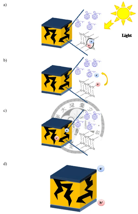
The active layer of polymer-based solar cells is composed of electron donor and acceptor. Solar cells transform light into electrical energy by exciting materials in active layer for carriers. The process is described through the following steps:
(1) Absorption of photos (Figure 1-1a):
In the first step, photos are absorbed and transform into energy, followed by photo-excitation of the electrons on donors. Sufficient and operative absorption from Solar Spectrum is required to generate more current. A band gap of 1.1 eV (1100nm) is capable of absorbing 77% of the solar irradiation.4 For this reason, developing new organic materials with small band gap is a way to enhance the performance of solar cells.
(2) Generation of charge carrier (excitons dissociation; Figure 1-1b):
Excitons diffuse to the interfacial area of electron donor and acceptor to dissociate. The diffusion length of excitons is around 10nm.10 Longer diffusion distance in donor increases the possibility of excitons’ recombination, which reduces the power conversion efficiency. Thus, controlling a proper morphology of active layer with nano-scale structure is quite important.
(3) Transport of the carriers to the electrodes (Figure 1-1c):
Dissociated excitons separate into holes and electrons, followed by diffusing
3
through the donor and acceptor to electrodes. A bicontinuously and interpenetrating passage of morphology and the property of materials with high carrier mobility are the essential terms to assist in transporting carriers.
(4) Collection of changes at the electrodes (generation of electric current; Figure 1-1d):
At last, optional electrodes with suitable work function have great effects on device operation. Inactive metals with low work function are proper for a cathode material. For anode, high work function conductor complemented with hole transporting layer is generally used.
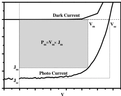
Through these four processes, polymer solar cells under sunlight can obtain currents. The current-voltage characteristics of a solar cell in the dark and under illumination are shown in Figure 1-2. Take the energy level schemes for example in Figure 1-3,11 when the solar cell is under illumination, incident sunlight photos are absorbed by the materials and generate excitons. Without an applied electric field (electrodes are connected and potential is zero, Figure 3a), the maximum current is so-called short current (Jsc) which is obtained at short circuited condition. Under an applied electric field, the gradient of materials’ work functions is offset, approaching no current flows. This voltage is defined as the open circuit voltage (Voc) at open circuit condition in Figure 3b.
4
Fill factor (FF) is defined as the ratio of the maximum power to the external short and open circuit value:
FF V J
V J
The external yield of energy conversion efficiency η (also called power conversion efficiency, PCE) is defined as the power produced by the cell (Pm) divided by the power incident on the rep sentative area of the cell (P ). re in
PCE P
P A 100% V J FF
Where:
Pin (incident light power density) =100mW/cm2 Ac (active surface area) =1cm2
Normally, PCE is the key parameter for solar cell’s productivity, and it is also the parameter often used for comparison purposes.11
Otherwise, for calibrating the experimental condition, light with an intensity of 1000 W/cm2 and a spectral distribution AM1.5 global standard solar spectrum were used.
5
a)
b)
c)
d)
Figure 1- 1 Working principle of bulk heterojunction solar cells: a) absorption of photos; b) Generation of charge carrier (excitons dissociation); c) Transport of the carriers to the electrodes; d) Collection of changes at the electrodes (generation of electric current).
6
7
Voc Vm
Jsc Jm
Dark Current
J
V Photo Current
Pm=Vm× Jm
Figure 1- 2 J-V curve of polymeric solar cells.
Figure 1- 3 Energy levels and light harvesting.11
1-3 The Bulk-Heterojunction Polymer Solar Cells
The evolution of polymer solar cells was through few kinds of structures, such as bilayer structure12,13, bulk heterojunctions14,15 and ordered heterojunctions16,17.
The bulk heterojunction (BHJ) is the most successful device architecture for polymeric
photovoltaic. In BHJ solar cells, the active layer is made of mixed donor and acceptor.
The mixed donor and acceptor may phase-separate and form a large area of interface.
Excitons can easily be dissociated when they diffuse to the nearby interface of donor
and acceptor. On the other hand, these phase-separated donor and acceptor in BHJ
provide bicontinuous and undisturbed pathways for the transport of charge carriers to the electrodes. Thus, we can realize that the key points to make high efficiency BHJ solar cells are: 1) control a proper morphology of active layer with nano-scale phase separation of electron donor and acceptor; 2) bicontinuous pathways of donor and acceptor for carrier transporting.
In these years, poly(3-hexylthiophene) (P3HT, shown in Figure 1-4) and phenyl-C61-butyric acid methyl ester (PCBM , shown in Figure 1-4) mixed BHJ solar cells have been studied extensively. The fullerene (C60) derivative PCBM is the the strongest candidate of electron acceptor materials used for organic photovoltaic application. PCBM plays an important role in separating the excitons and constituting the passways for electrons’ transportation. It has a high electron mobility
8
of 10-3 cm2/Vs.18 Most importantly, its good-solubility in solvent enlarges the processability in solution procedure.
As a hole conducting donor, P3HT have a relative low energy gap (1.9eV) which can absorb more photos in visible region. Highly-crystallized P3HT can approach high effect hole mobility in the range 0.05-0.1 cm2/Vs.19 It also has the advantages such as good solubility, processability, and environmental stability.20
Using region-regular P3HT (RR-P3HT) as donor and PCBM as acceptor, bulk heterojunction solar cells have been realized with external quantum efficiencies of around 75% and power conversion efficiencies up to 5%.21 It is proposed that the high efficiency of BHJ solar cells is due to the microcrystalline lamellar stacking of P3HT in the solid-state packing. It has also been improved by several techniques, such as pre-treatment of solution26, 27, 28, thermal annealing30, vapor annealing31, et al.
These processes all have a common purpose- control the morphology of active layer, which we introduce in following part.
Figure 1- 4 Chemical structure of PCBM (left) and P3HT (right).
9
1-4 Morphology Control for P3HT:PCBM BHJ Solar Cells
For P3HT: PCBM mixed system of polymeric solar cells, morphology control to active layer have a great influence on the performance and stability. Proper solvent to the P3HT and PCBM and annealing process to active layers are researched for controlling the crystallinity of P3HT and distribution of PCBM. According to different processes in active layer’s manufacture, it can be divided into two parts:
1-4-1 Solution treatments
As we know, solubility (affinity) of solvent to the solute makes a great effect in solutes’ aggregation or dispersion in solution. Thus, control the solubility of P3HT and PCBM solution is one of methods for their morphology control.
Good solvents for P3HT and PCBM like dichlorobenzene (DCB), chlorobenzene (CB)22, chloroform (CF)23 and toluene24 can supply a proper environment for P3HT and PCBM’s dissolving and extending. On purpose of increasing the crystallinity of P3HT, poor solvent can play a role of the nuclear agent while adding into a good solvent.25 For instance, poor solvent - hexane adding into DCB solution had an increased UV absorption peak at 607nm by P3HT’s aggregation.26 By the same idea, 3-hexylthiophene (3HT) in CB also can reduce the difficulty of P3HT’s nucleation.27
Besides solvents mixed system, using a proper poor-solvent also can increase the aggregation of P3HT. During an aging time, P3HT in both p-xylene28 and o-xylene29
10
can aggregates due to the natural poor-solubility.
P3HT fibers can be observed in solution by these processes. All processes mentioned above provide an increased crystallinity of P3HT and an improved efficiency. Besides, these solvent treatments take an annealing-free process in the device procedure.
1-4-2 Film treatments
In addition to solution treatments, making efforts to active layer during or after drying process also can effectively control the morphology of P3HT and PCBM.
Thermal-annealing is treated as a standard process for most solar cells’
manufacture. Thermal energy makes P3HT re-crystallized for approaching a high mobility. The most well-known process was developed by A. J. Heeger et al., which approached a power conversion of 5% by a 150oC post-annealing after Al cathode evaporated. Another process is solvent vapor annealing which prolong the wet time of active layer in drying process.30 During the evaporation of solvent, P3HT in good solvent such as DCB, may precipitate and self-arrange by the gradually increased concentration. This process was introduced by Y. Yang et al. and successfully obtained a solar cell performance with 4.37% efficiency.31 Thus, we understand that both re-crystallization and self-arrangement of P3HT assist in improving the device performance.
11
Besides to promote the crystallinity of P3HT, the distribution of PCBM is also an important issue for device performance. PCBM is a small molecule and easily terns to mobile and aggregate by any drive force such as thermal energy and lower solubility.
In lately study, Yang and his group added di-thioene into DCB solution. Di-thioene has an affinity to PCBM and higher boiling point than DCB. In film forming process, DCB will evaporate first, then (di-thioene) bring P3HT aggregating but PCBM still well-disperse in active layer. In this way, annealing-free process can be approached but without a large-scale aggregation of PCBM.32
In summary, how to control the morphology with high crystallinity of P3HT and well-distribution PCBM is the key point for approaching high performance device. It can be achieved by these mechanisms: solubility control, self-arrangement and re-crystallization of P3HT.
Even though these morphology-control processes can provide an increased performance of polymer solar cells, the further observation of morphology or device’s efficiency are rare to study. Morphology of active layer is facile to change with reducing effects for solar cells’ performance. It is known as “physical degradation”
introduced in section 1-5.
12
1-5 Degradation of P3HT:PCBM BHJ Solar Cells
In spite of the continuously efforts in promoting the efficiency of BHJ solar cells, the stability of the devices is also an essential issue for commercialization.
Various degradation processes occurring in BHJ solar cells. We classified this decay into physical and chemical parts.
1-5-1 Physical degradation:
In BHJ solar cells, physical degradation includes the diffusion of metal cathode33,34, interfacial contact35, and unstable morphology of active layer36,37. The issue we mostly concerned is the unstable morphology of active layer. As we mentioned above, mostly studies reported in promoting the performance of solar cells, but rare studies connected the relationship between morphology and device stability in different processes.
In first generation bulk heterojunction solar cells, study showed that “high Tg PPV” had a relatively better thermal stability of performance and bulk morphology than MDMO-PPV. This was interpreted that the free movement of the PCBM molecules was hampered due to a stiffer “high Tg PPV”: PCBM matrix.36 In recently study,
Jang Jo et al. reported that in P3HT: PCBM solar cells, solvent annealing resulted in a more stable morphology than thermal annealing. The key point was firm
and ordered P3HT can hamper PCBM’s large-scale aggregation, which was relatively
13
fast mobile by thermal energy.
37These studies provide us a good aspect about the mechanism of mobile P3HT and PCBM for improvement.
1-5-2 Chemical degradation:
On the other hand, chemical degradation in BHJ solar cells also includes several parts. The main causes of chemical degradation in BHJ solar cells come from ambient oxygen and water. It may oxidize low work function cathodes such as calcium (Ca) or aluminum (Al),38 photo-oxidized P3HT with light,39 or recover the natural acidic of Poly (3,4-ethylenedioxythiophene): poly(styrenesulfonate) (PEDOT: PSS) to un-stabilize the interface between PEDOT: PSS and Indium tin oxide (ITO) conductive glass.40 All chemical reactions mentioned above decrease the performance of solar cells. In the study, we focused on the degradation by unstable interface between ITO and PEDOT: PSS, which is rare known for its effect to BHJ solar cells.
PEDOT has been one of the most successful conducting polymers in organic electrical devices for its excellent transparency and high conductivity. In most application, PEDOT with PSS (Figure 1-5) is the most widely utilized because it has a good shelf life and can be easily coated on substrates. The existence of PSS has two functions. First, it can make charge balance to stabilize the p-doped PEDOT chains.
The other function is keeping PEDOT segments dispersed in aqueous medium
14
well.41,42
Though its good-stability of filmed PEDOT: PSS, it still unstable in humidity exposure by a reaction with ITO substrate. Hydrophilic PEDOT: PSS may absorb humidity to recover its acidic property.
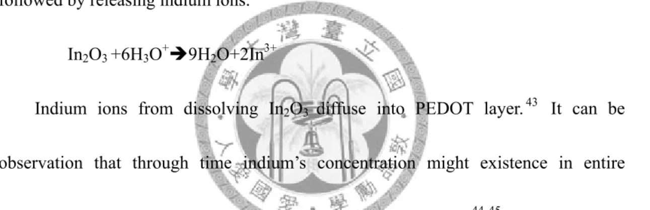
H2O+PSS(HSO3)ÎH3O++PSS(SO3)-
Conducting ITO is constituted with In2O3 and SnO2. In device structure, the acidic property of humidified PEDOT: PSS may etch the In2O3 in ITO substrate, followed by releasing indium ions.
In2O3 +6H3O+Î9H2O+2In3+
Indium ions from dissolving In2O3 diffuse into PEDOT layer.43 It can be observation that through time indium’s concentration might existence in entire PEDOT: PSS films even reach to the interface of the active layer.44,45
The phenomenon was first observed in polymer light emitting diode, but rare studied in solar cells.
Figure 1- 5 Chemical structure of PEDOT (bottom) and PSS (top).
15
1-6 Objective Statement
The goals of this research are two-fold: minimize the physical and chemical degradations of P3HT: PCBM BHJ solar cells, and maximize their power conversion efficiency. We accomplish our goals with two approaches: optimizing the active layer’s morphology by manipulating its film-forming process and eliminating anode/active layer reactions with an interface-modifying film deposited by atomic layer deposition (ALD).
In the first part (chapter 2), we focused on the physical degradation of morphology in active layer. New drying process at low temperature was adopted to approach a proper morphology. In addition to the observations of physical property, device performance and long-term stability also were examined.
In the second part (chapter 3), we make efforts in protecting the device from the unstable interface between ITO and PEDOT: PSS. To accomplish the objective, the concept of blocking layer was introduced. The effect of blocking layer inserted in the device was examined by long-term storage and depth-profile for observing the distribution of indium in thin films.
16
Chapter 2. Low-Temperature Drying Process
2-1 Introduction
As we know, the best way to retarded the physical decay of P3HT: PCBM mixed system solar cells is to control the morphology. How to maintain an stable morphology with well distributed P3HT and PCMB and high device performance are the key points.
Several studies have reported methods for obtaining a stiff morphology.
Examples among them include using crosslinkable conjugated conducting polymers46 as the active layer and adding a component with good compatibility to P3HT and PCBM to improve the blend morphology. However, these methods involve using new or additional materials in the solar cells and thus would increase the complexity of the fabrication process.
In this study, we developed a film-forming process for the P3HT: PCBM active layer that involved drying the films at a low temperature (-5oC) and thermally annealing them afterward, in the hope of increasing the crystallinity of P3HT and uniformity of the P3HT/PCBM blend. The morphological stability was tested by accelerated tests at elevated temperatures.
17
2-2 Experimental Section
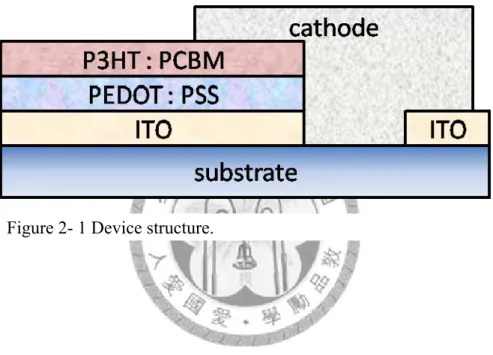
2-2-1 FabricationThe devices were fabricated in the following structure: ITO / PEDOT: PSS / P3HT: PCBM / Ca / Al, showed in Figure 2.1. First, the ITO-coated (~150 nm) glass substrates were cleaned by ultrasonic treatment in detergent, deionized water, acetone and isopropyl alcohol and by plasma for 15 minutes each step. Filtrated PEDOT: PSS by 0.20μm filter were spin-coated on the substrate with the thickness of 50 nm. The substrates were baked at 170oC for 15 minutes in air.
21mg P3HT and 21mg PCBM were dissolved in 1mL 1, 2-dichlorobenene (DCB) and stirred over 8 hours. The P3HT: PCBM mixed solvent were filtrated by a 0.20μm filter and spin-coated at 600 rpm for 30 seconds as the active layer (~200nm). The wet active layer was then subjected to the low-temperature drying process, where it was placed in sealed container at -5oC overnight for complete drying. The active layers of the control devices were dried at room temperatures instead.
The samples were annealed at 190oC for 2 minutes in nitrogen-filled glove box.
Then, 30nm of calcium and 100nm of aluminum were thermal evaporated on the top of the active layer as the cathode in vacuum (< 5x10⁻⁶ torr). The devices were encapsulated by UV glue with glass. The active area was 6.25 mm2, defined by a shadow mask.
18
Figure 2- 1 Device structure.
19
2-2-2 Measurement
The current-density-voltage (J-V) characteristics of the devices were measured in air with a Keithley 2400 source meter under simulated AM1.5G irradiation (100 mW cm−2) from a xenon-lamp-based solar simulator (Oriel 92250A-1000); the incident photon-to-electron conversion efficiency (IPCE) was measured with an Oriel® QE/IPCE measurement kit (including a 150W Xe arc light source, a CS260 monochromator, a lock-in amplifier, and a current preamplifier) with an aperture (1.77 mm2) covering the devices to eliminate extrinsic effects. TEM images of the P3HT:PCBM active layer were obtained with a JOEL JEM-1230 system using an accelerating voltage of 100 kV, with samples prepared by immersing cathode-less devices in deionized water to dissolve the PEDOT:PSS under-layer and lift off the P3HT:PCBM layer, and then collecting the floating P3HT:PCBM film with a copper grid. AFM images were obtained with a Veeco Multimode Scanning Probe Microscope operated in the tapping mode. X-ray diffraction (XRD) analysis was carried out using a PANalytical X’Pert Pro Powder Diffractometer with CuKα radiation. UV-Vis spectra were collected with a Jasco V-570 spectrometer.
20
2-3 Results and Discussion
21
2-3-1 Morphology of the Active Layer
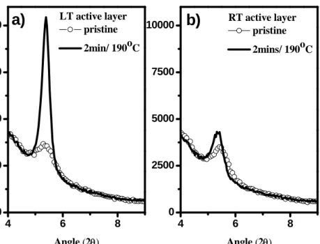
Figure 2-2 shows the X-ray diffraction pattern of P3HT/PCBM films on ITO/PEDOT: PSS substrate. The low-temperature-dried (LT) and the room-temperature-dried (RT) samples had equal intensity from the diffraction peak at 5.4o which is assigned to the (100) plane of the P3HT crystals. After a 190oC annealing for 2 minutes, as our expectation the RT samples had an increase in intensity of the (100) peak as a result of increased P3HT crystallinity from P3HT’s re-crystallization. It was interesting that the LT samples showed much more significant intensifying of the (100) peak.Moreover, as shown in Figure 2-3, the LT sample showed additional peaks after annealing: a secondary peak (200) at 10.8o and tertiary peak (300) at 15.9o,47 indicating that the LT films formed a well-organized intraplane structure. These two figures demonstrate that through a low-temperature drying process and thermal annealing, P3HT obtained a higher crystallinity with better ordering.
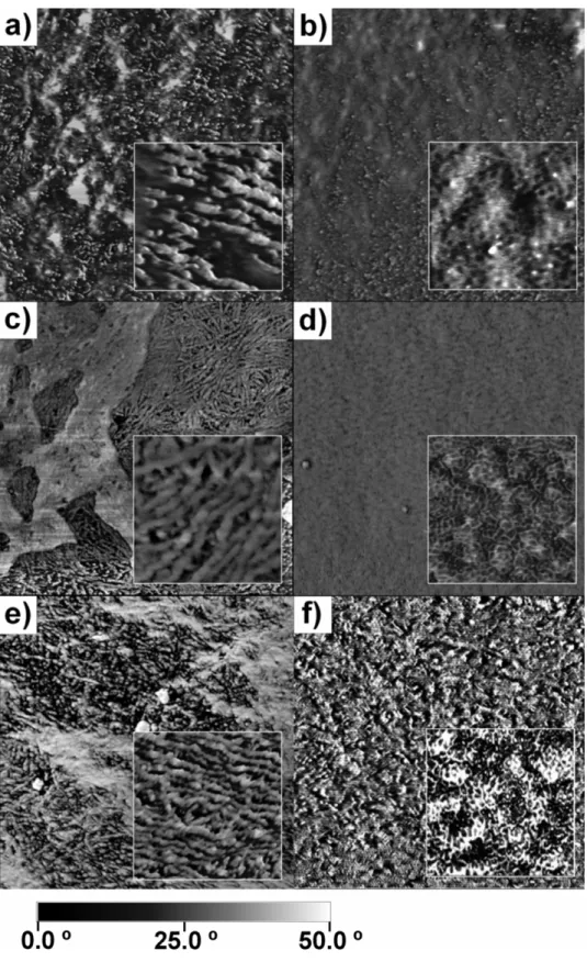
The morphology of the LT and RT layers was further analyzed with AFM. Figure 2-4 shows the AFM phase images for P3HT/PCBM films in two drying processes.
Before annealing (Figure 2-4a and 2-4b), the LT and RT layers had drastically different surface morphology despite their equal P3HT crystallinity as indicated by the XRD results. After thermal annealing for 2 minutes, re-crystallization made the
P3HT crystals more clearly observable at the surface. As can be seen by comparing Figure 2-4a with Figure 2-4c, the RT films contained ample P3HT fibers that were closely interlaced, which agrees with the typical morphology observed with P3HT:PCBM blends.48 However, such fibers were absent in the LT films, where pellets-like structures of P3HT appeared instead (see Figure 2-4b and Figure 2-4d).
We attribute the distinct morphology of the LT layer to enhanced crystal nucleation of P3HT during drying at low temperature. At the low temperature, the P3HT crystal nuclei were large in number and their simultaneous growth restricted the attainable size of the eventually formed crystals. Thus, small but dense P3HT crystal formed in the entire film. This morphology of P3HT in P3HT: PCBM blends was a novel discovery in the field of polymeric solar cells.
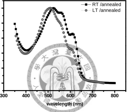
UV-vis spectra are also consistent with the size difference of the LT and RT P3HT crystals observed with AFM. The P3HT absorption peak is at 500 nm with a shoulder at 600 nm. The vibrionic absorption structures at 552 and 602 nm correspond to the π-π* interactions of the thiophene rings and its intensity increases with the size of P3HT crystallites.49 From the wavelength shape in Figure 2-5, these two peaks were apparent in the RT films, while they were much weaker in the LT films.
Besides P3HT’s crystallization, the distribution of PCBM in active layer is also an important concern for BHJ solar cells’ performance. This can be examined
22
with TEM, as P3HT appears brighter under TEM than PCBM due to its lower density (1.10 g cm-3 vs.1.50 g cm-3).50In the TEM images in Figure 2-6a and 2-6b, the contrast (between the brighter P3HT phase and the darker PCBM phase) of the before-annealing RT film was more evident than that of LT film. This indicates that in the RT drying process, P3HT and PCBM had stronger tendency to aggregate with the RT process than with the LT process. The lower tendency to aggregate of the LT process may be because P3HT and PCBM were forced to precipitate and freeze locally.
The variation of contrast of LT films upon annealing (from Figure 2-6b to Figure 2-6d) were more unobvious than that of RT films upon annealing (from Figure 2-6a to Figure 2-6c), which means that the P3HT and PCBM in LT process was more uniform than that in RT films during an annealing process. We inferred that the uniform distribution came from the enhanced nucleation of P3HT crystals in the LT drying process. The dense crystal nuclei of P3HT may obstruct the aggregation of the PCBM and the amorphous P3HT phases. Conversely, though RT films had larger-size P3HT, loose arrangement between P3HT fibers was hard to resist the aggregation of small molecule-PCBM which facilitated to move with a tiny volume. We expected that more stable and uniform active layer by LT drying process could provide better durability in performance of solar cells.
23
4 6 8 0
2500 5000 7500
10000 LT active layer
b)
pristine 2min/ 190oC
Intensity (a.u)
Angle (2θ)
a)
4 6 8
0 2500 5000 7500
10000 RT active layer pristine 2mins/ 190o
C
Angle (2θ)
Figure 2- 2 XRD patterns of a) the LT and b) the RT active layer, pristine (open circle) and after 2 min/190 ºC annealing (straight line).
10 20
0 2500 5000 7500 10000
(300) (200)
Intensity (a.u.)
Angle ( 2θ )
LT 2min/ 190oC RT 2min/ 190oC (100)
Figure 2- 3 XRD patterns of the LT (black circle) and RT (open circle) active layer after 2min/ 190oC.
24
Figure 2- 4 AFM of P3HT: PCBM film. RT films: a) pristine, c) 2min/190oC, e) stored at 65 ºC for 1368 h in vacuum, and LT films: b) pristine, d) 2min/190oC, f) stored at 65 ºC for 1368 h in vacuum. The image sizes are 3 × 3 μm for the main graphs and 0.5 × 0.5 μm for the insets. Samples for e) and f) were prepared by removing the cathode layers of the stored cells.
25
26
Figure 2- 5 UV-vis spectra of annealed RT (triangle) and LT (circle) films.
300 400 500 600 700 800
RT /annealed LT /annealed
Absorbance (a.u.)
wavelength (nm)
Figure 2- 6 TEM images of the active layer: a) RT without annealing; b) LT without annealing; c) RT with 2 min/190 ºC annealing; d) LT with 2 min/190 ºC annealing. The lengths of the scale bars are 5 μm in the main graphs, 50 nm in the insets.
27
2-3-2 Hole Mobility of the P3HT:PCBM Layer
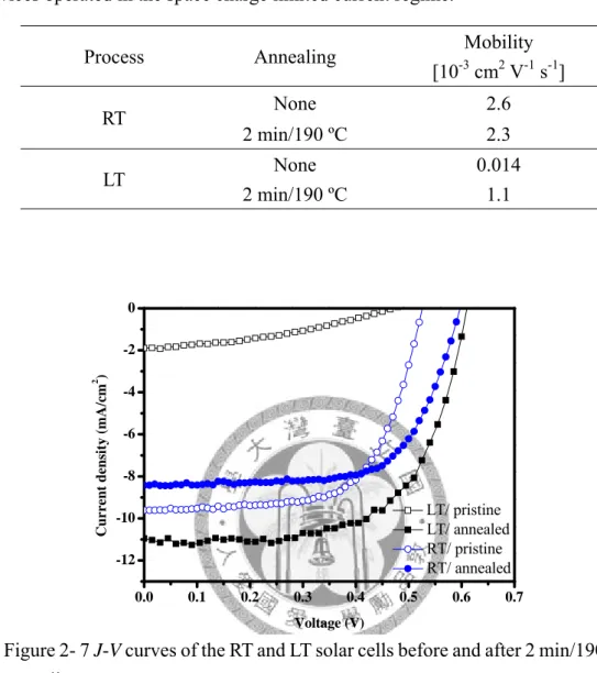
To confirm the hole mobility of P3HT: PCBM matrix layer with compatible value in BHJ solar cells, we measure the hole mobility shown in Table 2-1.
The hole mobility of LT/annealed films had almost two order improvement from 1.4x10⁻⁵ to 1.1x10⁻³ cm2/Vs than the pristine one. This enhancement was contributed to the increased and well-ordered crystallinity of P3HT in LT active layer, whose interconnected P3HT network would facilitate charge transport. On the other hand, RT dried P3HT: PCBM layers with and without annealing showed near values of hole mobility in same order. Although the increased P3HT crystallinity formed in RT/annealed active layer, slightly lowered hole mobility in RT/annealed films was caused by the over-aggregation of both P3HT and PCBM, reducing the charge transporting passways and interfacial area between donor and acceptor.
Thus we confirmed that LT/annealed P3HT: PCBM layer had the compatible hole mobility with RT dried active layer in the same order of value. The effects of hole mobility to P3HT:PCBM solar cells were introduced in following part.
28
29
2-3-3 Device Performance
Current density–voltage (J–V) measurements of solar cells by RT and LT process reveals in Figure 2-7 and Table 2-2. The pristine RT solar cells were as the standard, made with the same processing condition as reported elsewhere.51
Compare to the pristine RT cells, annealed RT cells had slightly decreased in Jsc . We contributed the descended Jsc came from the over-aggregation with reducing junctions and lower hole mobility shown in Table 2-1. Though Jsc decreased after annealing, the improved Voc maintained PCE at the average about 3.32%.
In contrast to the small change of RT device, LT device had a more than 5 times improvement of the Jsc (from 1.90 to 10.95 mA/cm2) after annealing. Increased PCE from 0.33% to 4.33% was also approached by LT drying process. The significantly improvement in current density and PCE was related to the increase of crystallinity of P3HT, which could be explained below by the experiment with different annealing temperatures.
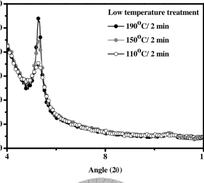
In Figure 2-8, P3HT’s crystallinity was increased with the annealing temperature.
This improvement was contributed from the characteristic of polymer crystallization.
The melt temperature (Tm) of P3HT was at 226.4oC. Under Tm, higher temperature supplies higher energy for P3HT chains moving to the surface of established P3HT nucleus, which can obtains higher crystallinity. High ordered P3HT in LT films approached a promoted hole mobility (shown in Table 2-1). Moreover, the compact
P3HT crystals could provide more junctions to dissociated excitons and unhindered passways to transport carriers, which might response to the increased Jsc (Table 2-2).
The greater efficiency of carriers transport in the LT-annealed cells also could be observed in IPCE curve. IPCE indicates the ratio of the number of photons incident on a solar cell to the number of generated charge carriers. As shown in Figure 2-9, the IPCE of LT/annealed cells showed a larger efficiency across all wavelengths than the RT/annealed cells. We contributed this high efficiency in LT/annealed films from the compact morphology and high-crystallized P3HT of LT cells’ active layer which can provide more junctions and passway for excitons’ dissociation to transport.
Besides, RT/annealed cells showed a different shape contrasted with LT/annealed cells in IPCE curve. RT/annealed cells had a relatively intensified efficiency around 550-600nm in IPCE, which was accordable to its UV-vis spectrum with a higher absorbance of peaks 552nm and 602nm, as the vibrionic absorption structure of P3HT.
On the contrary, this peaking toward 550-600nm was absent in the LT layer’s IPCE spectrum, conformed the result that the vibrionic absorption structures were weaker in the LT layer due to its small P3HT crystallites.
The enhancement of LT/annealed solar cells was proved from its high crystallinity of P3HT and compact morphology of active layer. Further, the stability of LT/annealed was examined in following part.
30
Table2- 1 Hole mobility of the RT and LT active layers, measured with hole-only devices operated in the space charge limited current regime.
Mobility Annealing
Process
[10-3 cm2 V-1 s-1]
None 2.6
RT 2 min/190 ºC 2.3
None 0.014
LT 2 min/190 ºC 1.1
0.0 0.1 0.2 0.3 0.4 0.5 0.6 0.7
-12 -10 -8 -6 -4 -2 0
Current density (mA/cm2 )
Voltage (V)
LT/ pristine LT/ annealed RT/ pristine RT/ annealed
Table2- 2 Summary of device performance of ITO/PEDOT: PSS/ P3HT: PCBM/Ca/Al polymer solar cells with different fabrication conditions.
JSC VOC FF PCE
Annealing Process
[mA cm-2] [mV] [%] [%]
none 9.61 0.53 64.1 3.27
RT 2min/190oC 8.43 0.60 66.7 3.37
none 1.90 0.48 36.0 0.33
LT 2min/190oC 10.95 0.62 64.3 4.33
Figure 2- 7 J-V curves of the RT and LT solar cells before and after 2 min/190 ºC annealing
31
4 8 0
1000 2000 3000 4000 5000 6000
12
Intensity (a.u.)
Angle (2θ)
Low temperature treatment 190o
C/ 2 min 150o
C/ 2 min 110o
C/ 2 min
Figure 2- 8 XRD patterns of the LT active layer after annealing: 110oC/ 2min (open circle), 150 ºC/ 2min (gray circle), and 190oC/ 2min (black circle).
Table2- 3 Summary of device performance of ITO/PEDOT: PSS/ P3HT: PCBM/Ca/Al polymer solar cells by low-temperature drying process with different annealing conditions.
JSC VOC FF PCE
Annealing Process
[mA cm-2] [mV] [%] [%]
2min/110oC 9.00 53.1 52.7 2.51
2min/150oC
LT 10.00 58.6 58.0 3.40
2min/190oC 11.50 61.5 62.8 4.43
32
300 400 500 600 700 800 0
20 40 60 80 100
IPCE (%)
Wavelength (nm)
RT /annealed LT /annealed
Figure 2- 9 IPCE spectra of the RT and LT cells (annealed at 190 ºC for 2 min).
33
2-3-4 Device Stability
Another issue for BHJ solar cells is the stability. As we know that polymers tend to change their morphology with through time and temperature. This characteristic of P3HT may provide an unstable morphology in active layer with further aggregation of P3HT and PCBM, decreasing the performance of BHJ solar cells by reducing the junctions. Thus, the stability of BHJ solar cells is needed to be concerned.
The first test was whether the morphology of P3HT: PCBM active layer can against longer term of annealing. As shown in Table 2-4, after a 30minuits annealing, RT cells had a 23 % degrade of PCE from 3.23% to 2.49%. However, LT devices had a less degraded rate with 10% decay from 4.07% to 3.70%. We demonstrated the decayed-variation between RT and LT cells came from the different active layer morphology. LT cells had a compact structure of P3HT in active layer, which could efficiently prevent the further migration of PCBM during thermal annealing. On the contrary, larger but less P3HT fibers provided a loose network in RT active layer, which was hard to prohibit the migration of PCBM and obtained a worse performance of BHJ solar cells after longer annealing. The more stable BHJ cells with better performance by LT process also approached in the accelerated test with long-term storage.
Accelerated test were operating in vacuum at 65 ºC over 1300 hr. Original PCE
34
of LT and RT devices were 4.43% and 3.23%. The result is shown in Figure 2-10 and Table 2-5. After 1368 hr, LT cells maintained a 2.15% PCE in performance. From AFM figures, LT/annealed active layer (Figure 2-4f) showed a less phase separation between P3HT and PCBM. However, such morphological stability was absent in the RT layer (Figure 2-4e), as it developed pronounced phase separation upon annealing or extended heating. Also, the RT device showed a severer degraded over 80% from 3.23% to 0.45% during this storing period.
Thus, the morphological stability of LT active layer was verified. BHJ solar cells by LT process not only approached a high efficiency, but also provide a stable performance by its stiff active layer.
35
Table2- 4 Device performance of ITO/PEDOT:PSS/ P3HT:PCBM/Ca/Al polymer solar cells with different anneing temperature.
JSC
[mA cm-2]
VOC
[mV]
FF [%]
PCE Annealing [%]
Process
2min/190oC 8.41 0.59 65.4 3.23 RT
30min/190oC 8.25 0.57 53.3 2.49
2min/190oC 10.60 0.62 62.0 4.07
LT
30min/190oC 9.87 0.61 61.4 3.70
0 500 1000 1500
0 1 2 3 4
PEC (%)
Storage time (hr)
RT / annealed LT/ annealed
Table 2- 5 Device performance of ITO/PEDOT: PSS/ P3HT: PCBM/Ca/Al polymer solar cells in accelerated test. Annealing applied to complete, encapsulated devices stored in vacuum.
Storing condition JSC
[mA cm-2]
VOC
Process
[mV]
FF [%]
PCE [%]
RT none 8.41 58.7 65.4 3.23
1368 h/65 ºC 2.48 48.7 37.2 0.45
none 11.50 61.5 62.8 4.43
LT 1368 h/65 ºC 7.28 54.2 54.4 2.15
Figure 2- 10 Degradation of the power conversion efficiency during storage at 65 ºC in vacuum: RT/annealed (circle) and LT/annealed (square).
36
2-3-5 Models of the LT and RT Morphology
Combine with the results mentioned above, we proposed models of the LT and RT morphology in the following and illustrated it in Figure 2-11
Drying process of P3HT in active layers is constructed from two steps: P3HT’s nucleation and growth. In most used procedure for controlling P3HT: PCBM’s morphology (Figure 2-11a), prolong the drying time is effective to make P3HT’s self-arrangement well which just grows along the established P3HT nucleus. The number of P3HT nucleus is according to the concentration of wet active layer at fixed temperature. In thermal annealing step, PCBM had a great affinity to aggregate, which may compete with P3HT’s migration. The large-scale aggregation of both P3HT and PCBM may decrease the amount of junctions and carrier’s passways, bring in a lower performance and worse durability for BHJ solar cells.
37
In this study, we reduced the temperature to -5oC in drying process to lower the critical concentration of P3HT: PCBM solution in film condition. During LT drying process, P3HT was forced to precipitate (Figure 2-11b); meanwhile both P3HT and PCBM molecular froze until the DCB solvent completely vaporized. Nucleation of P3HT dominated over the LT drying process. In annealing procedure, polymer chains of P3HT could easily approach to the surface of plentiful P3HT nucleus for crystallization, supplying higher crystallinity. Furthermore, these growing P3HT had larger competence to resist the migration of small molecular PCBM. It could afford a
high uniformity and stability in P3HT: PCBM morphology even promotes the performance and durability in BHJ solar cells.
38
Figure 2- 11 Proposed model during annealing process. White region:
PCBM-rich domain; Black region: amorphous P3HT-rich domain; Gray wire:
P3HT crystal.
39
2-4 Summary
In this chapter, we develop a novel process – low-temperature drying process, for manufacturing P3HT: PCBM BHJ solar cells. This LT process effectively assists in the nucleation of P3HT in active layer. After annealing, a quite high crystallinity of P3HT with a densely interconnected network and more uniform distribution of PCBM were obtained in the active layer.
The compact morphology and highly crystallized P3HT in the active layer resulted in increased efficiency and current density through their more efficient exitons dissociation and carrier transport. Meanwhile, the more stable morphology of the LT active layer obstructed aggregation of PCBM, achieving high durability BHJ solar cells.
The findings of this study offer effective solution to the key issues of the P3HT/PCBM-based polymer solar cells: stability and efficiency.
40
Chapter 3. ALD Blocking Layer
3-1 Introduction
In this chapter, we discuss our study to eliminate the degradation caused by the unstable interface between ITO and PEDOT: PSS. As mentioned in section 1-4-2, acidic PEDOT: PSS may etch the In2O3 in ITO substrate, followed by the diffusion of indium.
The effects of the chemical reaction of ITO with the PEDOT: PSS layer have been reported. Kawano et al. reported that with water absorption into the PEDOT:
PSS, the resistivity of the PEDOT: PSS/blend layer interface increased due to ITO reaction with PEDOT: PSS.35 Additionally Chen et al. showed that a decrease of ionization potential (IP) of PEDOT: PSS was detected due to dedoping of the PEDOT resulting from a reaction of PSS with ITO in the presence of water.52
The effects of the ITO/PEDOT: PSS reaction have been reported for polymer light emitting diode, which showed lower brightness and current density as a consequence of such reaction. However, the effect of this reaction on solar cells has not been studied. Thus, it was our objective to address this unexplored issue..
Several approaches have been developed to prevent the occurrence of the ITO/PEDOT: PSS reaction. One approach is to add glycidoxypropyl trimethoxysilane
41
(GPS) to PEDOT followed by annealing, upon which the PEDOT film becomes a crosslinked network,53 which prevents indium diffusion from the ITO electrode.
Another approach is to treat the ITO surface with compounds such as (NH4)2Sx54 and self-assembly monolayer,55which can diminish the reactivity of ITO/PEDOT: PSS interface. However, the practicalities of these approaches are limited by their complicated process, poor uniformity, and inadequate suface coverage.
For this reason, we selected atomic layer deposition (ALD) to form a blocking layer. ALD deposits inorganic thin film through chemical reaction with alternative precursors, showed in Figure 3-1. The advantages of ALD process are: (1) Large area thickness uniformity; (2) Accurate thickness control within a monolayer; (3) Capability of depositing defect-free films; (4) 100 % step coverage. Through these benefits, we believe it has great potential to form a well protecting layer.
For the material of blocking layer, hafnium oxide (HfO2) thin film by ALDhas been reported with good hydrophobia and anticorrosive. We inserted HfO2 in P3HT:
PCBM solar cells as a blocking layer. Its well-coverage and anticorrosive have the potential against acidic PEDOT: PSS. The insert layer in PEDOT also has been reported with an improved PCE and current density in solar cells’ performance.57 Thus, we expected the ALD HfO2 inserted in structure may effectively promote the performance also retarded the degradation of solar cells.
42
Two structures introduced for studying: HBH structure (ITO/PEDOT:
PSS/HfO2/PEDOT: PSS/active layer/Ca/Al) and BH structure (ITO/ HfO2/PEDOT:
PSS/active layer/Ca/Al). Here, H is abbreviated from hole transporting layer, which is the function of PEDOT: PSS; B is the abbreviation of blocking layer.
43
Figure 3-1 Schematic illustration of an ALD growth cycle (1–4) leading to the formation of a binary oxide film of metal (○) and oxygen (●). L refers to the precursor ligand.56
44
3-2 Experimental Section
3-2-1 FabricationThe device structure is showed in Figure 3-1. The fabrication of devices was as same as section 2-2-1 except the thickness of PEDOT: PSS layer with and without HfO2 was controlled at 60nm, annealing temperature of PEDOT: PSS was at 150oC for 150min.
ALD HfO2 thin films were grown in Cambridge Nanotech Savannah 100 ALD system. Tetra-dimethyl amino hafnium (TDMAHf) and water (H2O) were selected as the precursor of HfO2. Deposition process was operated at 150oC of chamber temperature. ALD recipe of HfO2 was showed below:
Table 3- 1 The operating condition of ALD deposited HfO2. Pulse time Exposure time
[s]
Pumping time precursor
[s] [s]
H2O 0.02 0 7
TDMAHf 0.1 0 7
The procedure of durability test was shown in Figure 3-X. Semi-cells with PEDOT: PSS and active layer were storage at 28oC and 60% relative humidity for several weeks. Before metal cathode evaporated on device, a 100oC annealing for 1hr was utilized.
45
Figure 3-2 Device structures: (A) conventional structure; (B) HBH structure;
(C) BH structure. (H: hole transporting layer; B: blocking layer)
46
47
b) a)
c)
Figure 3- 3 Storage condition and process of degradation test: a) storage; b) discharge residual water; c) evaporation of cathode.
3-2-2 Measurement
The current-density-voltage (J-V) characteristics of the devices were measured in air with a Keithley 2400 source meter under simulated AM1.5G irradiation (100 mW cm−2) from a xenon-lamp-based solar simulator (Oriel 92250A-1000);
Thickness of HfO2 was measure by Alpha-Step surfcorder (Kosaka Lab. Ltd.
Surfcorder ET-3000). Thickness of HfO2 per cycle was measure from the HfO2 films with 500 cycles, deposited on ITO substrates.
Auger Electron Spectroscopy (AES) surface profile of PEDOT was obtained by VG Scientific,Microlab 350 and operated at 3kV.The sample was in the structure of ITO/PEDOT, storing in dry box for three months.
Depth profile of x-ray photoemission spectroscopy (XPS) were measure by Thermo Scientific K-Alpha with the sputter energy of 3keV. The XPS sample was stored at 28oC and 60% relative humidity with the structure: ITO/ (HfO2, 1nm)/PEDOT: PSS (~60nm)/active layer (~100nm).
48
3-3 Results and Discussion
3-3-1 Verification of Indium Diffusion
To verify the phenomenon about indium diffusion in PEDOT: PSS layer, the surface survey of the main elements of PEDOT: PSS was detected by Auger Electron Spectroscopy (AES). In the range of electron energy from 100eV to 600eV, the components of sulfur (S) at 152eV, carbon (C) at 272eV, and oxygen (O) at 503eV are the elements what the PEDOT: PSS composed of.56 And indium (In) at 404eV is the target which we judge whether the reaction between ITO and PEDOT: PSS occurred.
After storing at 28oC and 60% relative humidity for three months, the indium signal contained in the surface of PEDOT: PSS films in Figure 3-4. The original and 1st differential data of AES indicates that indium which released from the reaction of ITO and PEDOT: PSS diffused through the entirely PEDOT: PSS to the surface.
This result corresponds with previous literatures and confirms the importance of prohibiting indium’s diffusion.
49
100 200 300 400 500 600 0
50000 100000 150000 200000 250000
O In
Electron energy (eV)
N
S C
-2500 -2000 -1500 -1000 -500 0 500
dN/dE
Figure 3-4 AES survey of top PEDOT: PSS stored in air for three months: origin data (bottom) and 1st differential data (top).
50
3-3-2 HBH Structure
Firstly, we optimized the thickness of HfO2 blocking layer. The thickness of HfO2 each cycle was 1.3Å. As shown in Figure 3-5 and Table 3-2, the best thickness of HfO2 in HBH structure was 1.9 nm (15 cycles). With the optimized thickness, the performance in HBH structure had a better performance in both Jsc and PCE than the conventional one. The PCE and Jsc were increased from 10.00 mA/cm2 and 3.34% to 11.33 mA/cm2 and 3.46% respectively. This enhancement of Jsc and PCE was due to the promoted inner electrical field, which has been reported in Al2O3 formed HBH structure.57 Tsai et al. indicate that upper PEDOT and original one in HBH structure have different work functions of 5.6 eV and 5.43eV. Larger difference of work function between cathode and anode can provide a higher electrical filed, assisting in carriers transporting for higher current density.
As an insulator, thicker HfO2 over 2nm (15 cycles of ALD) prevented carrier transporting via tunneling. As shown in Figure 3-5 and Table 3-2, device performance deteriorated severely into a quite low PCE of 0.39% and Jsc of 3.15 mA/cm2. Thus we chose the critical thickness – 1.9 nm of HfO2 (15 cycles by ALD) as our thickness of blocking layer in HBH structure, expected its advantages of enhanced current density and good protection.
To clarify the effect of out-diffused indium from ITO to the performance of solar
51
cells, devices without metal cathode stored at 28oC and 60% relative humidity to allow the chemical reaction between ITO and PEDOT: PSS to occur. Other decay-causing factors such as light and residual water absorbed in storage were prevented by storing in dark and annealing after storage respectively.
The storing test is showed in Figure 3-6 and Table 3-3. Degradation of conventional devices without HfO2 had a 12.6% degraded PCE from 3.72% to 3.25%
after 3 weeks storage. Both Jsc and Voc decreased in the range of 10%. We interpreted the descents of conventional cells resulted from the unstable interface of PEDOT: PSS and other unavoidable factors: surface contamination, morphology change. We expected that the HBH cells we introduced might efficiently obstruct indiums across through the HfO2.
However, unfortunately HBH cells had a 37.6% degraded PCE from 3.76% to 2.32%, which was worse than that of conventional devices (Figure 3-7 and Table 3-3).
Based on all constant controls, the worse performance of HBH cells, we explained, was attributed to the destruction of HfO2 by the swelling of PEDOT: PSS. As we know, the swelling of polymer may increase its surface roughness,58 which is easily higher than what the inorganic thin film can bear. Also, the roughness and film quality of PEDOT: PSS are larger responsible for its transporting function.59 Instead of serving as a protection, the crumbled HfO2 layer worsened the film quality and thus
52