Convergence of hot-carrier-induced saturation-region drain current
and linear-region drain current degradation in advanced
n
-channel
metal–oxide–semiconductor field-effect transistors
Jone F. Chena)and Chih-Pin Tsao
Department of Electrical Engineering and Institute of Microelectronics, National Cheng Kung University, Tainan, Taiwan 70101, Republic of China
共Received 13 March 2003; accepted 30 June 2003兲
The relationship between hot-carrier-induced drain current degradation and characterization drain voltage is investigated in n-channel metal–oxide–semiconductor field-effect transistors fabricated using 0.18m technology. The results show that the maximum drain current degradation occurs at a characterization drain voltage that is higher than 0.1 V. This finding is attributed to two competing mechanisms as the characterization drain voltage increases: the reduction in channel inversion charges and the reduction in charged interface states. The convergence of the saturation-region drain current and linear-region drain current degradation is more evident when the device is under stress at higher temperature and forward body bias. © 2003 American Institute of Physics.
关DOI: 10.1063/1.1605247兴
Hot-carrier reliability of n-channel metal–oxide– semiconductor field-effect transistors (n-MOSFETs) has been investigated extensively since it is a major reliability concern as devices are scaled.1–3Linear-region drain current (Idlin) or saturation-region drain current (Idsat) is frequently
monitored to quantify the impact of hot-carrier-induced dam-age on characteristics of the device. Idlinis usually measured
under gate voltage (Vg) equal to supply voltage (Vdd), and
drain voltage (Vd) equal to 0.1 V. Idsat is characterized by
Vg⫽Vd⫽Vdd. Traditionally, Idlin exhibits more severe
radation and is usually used as a monitor of worst-case deg-radation. Idsatdegradation, however, has been shown to
cor-relate with circuit speed degradation better.4Since devices in a circuit experience various Vd during gate switching, it is useful to study the behavior of drain current degradation (⌬Id/Id) for characterization of Vdbetween 0.1 V and Vdd.
Thus, this letter investigates the effect of characterization of
Vd on the magnitude of⌬Id/Id in advanced n-MOSFETs.
n-MOSFETs with 0.18 and 0.24m gate lengths共L兲 and 4 nm gate oxide thickness were fabricated using advanced 0.18 m dual-polygate complementary metal–oxide– semiconductor technology. Another n-MOSFET with L ⫽0.24m and 5 nm gate oxide thickness fabricated using 0.25 m dual-polygate complementary metal–oxide– semiconductor technology was also characterized for com-parison. The gate width of the devices is 10 m. The forward-mode drain current (Id) measured at Vg⫽Vdd at
various Vd was monitored. Vdd is 1.8 V for 0.18 m tech-nology, and 2.2 V for 0.25 m technology. Accelerated dc stressing was performed under various Vd, Vg, body bias
(Vb), and temperatures under the following ranges: Vdfrom
2.6 to 3.6 V, Vg from 0.7 to 4.1 V, Vb from 0 to 0.8 V, and temperatures from 25 to 125 °C. Stressing was performed for 50 min and interrupted periodically to measure ⌬Id/Id.
Idlinand Idsatdegradation of the L⫽0.18m device
fab-ricated using 0.18 m technology and the L⫽0.24m de-vice fabricated using 0.25 m technology stressed under
Vd⫽2.6 and 3.6 V, Vg at peak substrate current (Isub) and 25 °C is shown in Fig. 1. The results show that Idlinand Idsat
degradation can be described by a power law, ⌬Id/Id
⫽Atn, for both kinds of devices. However, the results in Fig.
1 also indicate that the difference between the magnitude of
Idsatdegradation and Idlin degradation is less for the device
fabricated using 0.18m technology. This trend is more evi-dent, as seen in Fig. 2. The ratio of Idsatdegradation to Idlin degradation for the devices in Fig. 1 is around 0.7 and 0.4 for 0.18 and 0.25m technology, respectively.
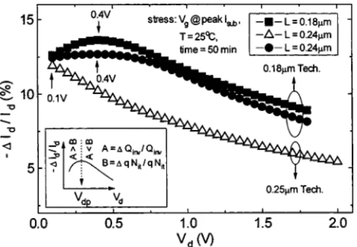
To examine this phenomenon, hot-carrier-induced ⌬Id/Idas a function of characterization of Vdfor the devices
in Fig. 1 under stress for 50 min is analyzed and shown in Fig. 3. Also, the data for a L⫽0.24m device fabricated using 0.18 m technology stressed for 50 min under Vd
⫽3.1 V and Vg at peak Isub is included in Fig. 3 for com-parison. As shown in Fig. 3, a monotonical decrease in ⌬Id/Id 共this trend is consistent with data published in the
past5,6兲 is observed for the L⫽0.24m device fabricated
a兲Electronic mail: [email protected]
FIG. 1. Idlinand Idsatdegradation for n-MOSFETs fabricated using 0.18 and
0.25m technology. The difference between the magnitude of Idsat
degra-dation and Idlindegradation is less for the device fabricated using 0.18m
technology.
APPLIED PHYSICS LETTERS VOLUME 83, NUMBER 9 1 SEPTEMBER 2003
1872
0003-6951/2003/83(9)/1872/3/$20.00 © 2003 American Institute of Physics
using 0.25m technology. This trend has been explained by lowering of the quasi-Fermi level and the masking effect of the velocity saturation region 共VSR兲.5 However, a skewed bell shape in ⌬Id/Id is observed for both the L⫽0.18 and
0.24m devices fabricated using 0.18m technology. Since the L⫽0.24m device fabricated using 0.18m technology also exhibits a skewed bell shape in⌬Id/Id, Fig. 3 indicates
that this new trend in⌬Id/Id is not attributed to a shorter L,
but is related to advanced technology.
To investigate this trend in ⌬Id/Id, an Id degradation
model, modified from that given by Aur and Chapman,7 is adopted:
⌬Id/Id⬇⫺共Lit/L兲⫻共qNit/Qinv兲, 共1兲
where Lit is the length of the damage region, qNit is the
number of charged interface states, Qinv⫽⫺Cox(Vg⫺VT
⫺Vc) is the number of channel inversion charges, Coxis gate oxide capacitance, VTis threshold voltage, and Vcis channel potential. Note that both qNitand Qinvare functions of char-acterization of Vd. In Eq. 共1兲, two competing mechanisms exist as the characterization of Vd increases. First, qNit de-creases because of lowering of the quasi-Fermi level. This mechanism results in the reduction of⌬Id/Id.5Second, Qinv
also decreases since Vcincreases. This mechanism results in
the increase of⌬Id/Id. According to the analysis above, the
relative rate of reduction in Qinv(⌬Qinv/Qinv) and reduction in qNit (⌬qNit/qNit) determines the value of
characteriza-tion of Vd at which maximum ⌬Id/Id occurs (Vd p) as
de-picted in the inset of Fig. 3.
To explain the increase in Vd p for devices fabricated using 0.18m technology, the effect of an increase in char-acterization of Vd on ⌬Qinv/Qinv was examined. Assuming the increase in characterization of Vd (⌬Vd) is small, the
rate of reduction in channel inversion charges near the drain edge can be approximated by ⌬Qinv/Qinv⬇⫺⌬Vd/(Vg
⫺VT⫺Vd). This indicates that when Vd and⌬Vd are fixed,
smaller (Vg⫺VT) results in larger 兩⌬Qinv/Qinv兩. This trend
leads to relatively greater ⌬Id/Id (Vg⫺VT) of the devices
fabricated using 0.18 and 0.25 m technology in Fig. 1 was then extracted and the results are 1.42 and 1.74 V, respec-tively. Thus, devices fabricated using 0.18 m technology have smaller (Vg⫺VT), resulting in greater⌬Qinv/Qinvand higher Vd p. Note that any smaller value of (Vg⫺VT) may
not necessarily produce higher Vd p because ⌬qNit/qNit is
also a function of Vg and Vd such that the condition
兩⌬Qinv/Qinv兩⬎兩⌬qNit/qNit兩 may not always hold.
To probe this observation further, the L⫽0.24m de-vice fabricated using 0.18 m technology were stressed for 50 min under Vd⫽3.1 V and Vg at peak Isub with various temperatures and Vb. According to the results of stressing,
the stress condition to produce higher Vd p and its effect on
⌬Id/Id vs Vd characteristic can be analyzed. It was found
that devices stressed at higher temperature and forward body bias produce higher Vd p and a flatter⌬Id/Id vs Vd
charac-teristic as seen in Fig. 4. This result can be explained by the following three reasons. First, the damage region is located further away from the drain under high temperature stressing.8Second, devices stressed under forward body bias can produce a wider damage region because carriers obtain higher energy through the process of Auger recombination.9 Due to these two effects, less qNitis affected by lowering of
the quasi-Fermi level and兩⌬qNit/qNit兩 is relatively smaller.
Third, devices operated under higher temperature result in shorter VSR.6At a fixed value of Idlindegradation, a shorter FIG. 2. Ratio of Idsatdegradation to Idlindegradation for the devices shown
in Fig. 1. This ratio is closer to unity for the device fabricated using 0.18m technology.
FIG. 3. Relationship between ⌬Id/Id and characterization of Vd for
n-MOSFETs fabricated using 0.18 and 0.25m technology. The character-ization of Vdto produce the maximum of⌬Id/Idis higher than 0.1 V for the
devices fabricated using 0.18m technology.
FIG. 4. Relationship between ⌬Id/Id and characterization of Vd for
n-MOSFETs fabricated using 0.18m technology stressed under various temperatures and Vb. A flatter shape is observed when the device is stressed
under higher temperature and forward body bias.
1873
Appl. Phys. Lett., Vol. 83, No. 9, 1 September 2003 J. F. Chen and C. Tsao
VSR would produce greater Idsat degradation because the
masking effect of VSR is reduced. Such an effect further results in a flatter ⌬Id/Id vs Vd characteristic.
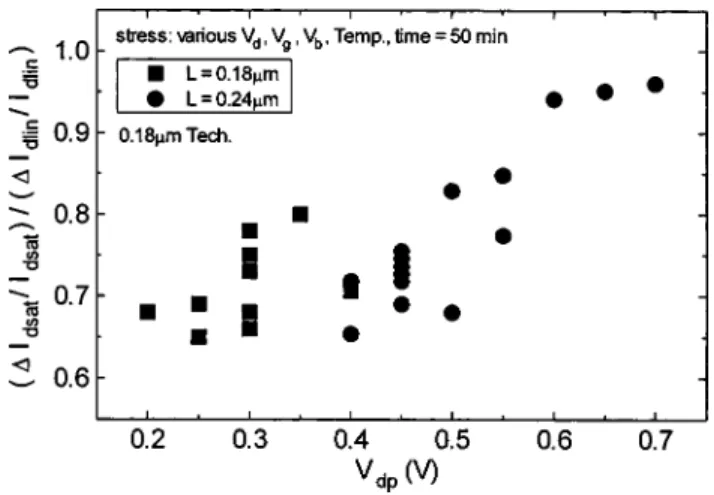
Because higher Vd p is concurrent with a flatter ⌬Id/Id
vs Vdcharacteristic, seen in Fig. 4, it is interesting to
exam-ine the relationship between the magnitude of Vd p and the ratio of Idsatdegradation to Idlindegradation. Figure 5 shows the results for 29 devices fabricated using 0.18m technol-ogy stressed for 50 min at various Vd, Vg, Vb, and tempera-tures. A clear trend is seen that higher Vd presults in a ratio
that is closer to unity even if the stress condition is varied. In
other words, the magnitude of Idsatdegradation would
con-verge to the magnitude of Idlin degradation when Vd p is
higher.
In summary, the convergence of hot-carrier-induced Idsat
degradation and Idlin degradation was observed in
n-MOSFETs fabricated using 0.18 m technology. Devices stressed at higher temperature and forward body bias exhibit a flatter ⌬Id/Id vs Vd characteristic. Id characterized at Vd
⫽0.1 V may no longer produce the maximum of ⌬Id/Id. To
find the worst-case Iddegradation, Idshould be characterized
under various Vd in each period of stress.
The authors would like to thank T. C. Ong of TSMC for helpful discussions. This work was supported by the Na-tional Science Council under Contract No. NSC91-2215-E006-015.
1E. Takeda and N. Suzuki, IEEE Electron Device Lett. 4, 111共1983兲. 2C. Hu, S. C. Tam, F. C. Hsu, P. K. Ko, T. Y. Chan, and K. W. Terrill, IEEE
Trans. Electron Devices 32, 375共1985兲. 3
P. Bellens, P. Hermans, G. Groeseneken, and H. E. Maes, IEEE Electron Device Lett. 9, 232共1988兲.
4K. Quader, P. Ko, and C. Hu, Tech. Dig. - Int. Electron Devices Meet., 511 共1993兲.
5K. N. Quader, C. C. Li, R. Tu, E. Rosenbaum, P. K. Ko, and C. Hu, IEEE Trans. Electron Devices 40, 2245共1993兲.
6H. Hwang, J. S. Goo, H. Kwon, and H. Shin, Proceedings of the Interna-tional Reliability Physics Symposium, 1995, p. 48.
7S. Aur and R. A. Chapman, Proceedings International Reliability Physics Symposium, 1994, p. 48.
8
E. Li, E. Rosenbaum, L. F. Register, J. Tao, and P. Fang, Proceedings of the International Reliability Physics Symposium, 2000, p. 103. 9L. P. Chiang, C. W. Tsai, and T. Wang, Proceedings VLSI Technology,
2000, p. 132.
FIG. 5. Relationship between Vd pand the ratio of Idsatdegradation to Idlin
degradation for n-MOSFETs fabricated using 0.18m technology stressed under various Vd, Vg, Vb, and temperatures. This ratio is closer to unity as
Vd pincreases.
1874 Appl. Phys. Lett., Vol. 83, No. 9, 1 September 2003 J. F. Chen and C. Tsao