Flicker Noise of AlGaN/GaN Metal-Oxide-Semiconductor
Heterostructure Field-Effect Transistor with a Photo-CVD
SiO
2Layer
C. H. Liu,a K. T. Lam,bS. J. Chang,c,zC. K. Wang,cand Y. S. Sund a
Department of Electronic Engineering, Nan Jeon Institute of Technology, Yan-Hsui 737, Taiwan b
Department of Information Communication, Leader University, Tainan 701, Taiwan c
Institute of Microelectronics and Department of Electrical Engineering, Advanced Optoelectronic Technology Center, National Cheng Kung University, Tainan 70101, Taiwan
d
Department of Materials Science and Engineering, China University of Petroleum, Dongying City, Shandong 257061, China
The effects of drain-source distance and applied voltage on low-frequency noise behavior of AlGaN/GaN metal-oxide-semiconductor heterostructure field-effect-transistors incorporated with a photochemical vapor deposited共photo-CVD兲 SiO2gate oxide layer were investigated. According to our studies, the normalized noise power density is inversely proportional to L⬘ 共=Ld-s− Lgate兲 when devices are biased in the linear region. However, the drain-source distance alone exerts little influence on low-frequency noise in the saturation and cutoff regions. Furthermore, the 1/f⌫noise characteristics and the⌫ value were affected by the interface state distribution in the energy bandgap as the gate bias was varied. The normalized noise power density determined is independent of the drain-source voltage in the linear region, but it exhibits an enhancement in the saturation region in response to an increase in the drain-source voltage. However, the noise power density then becomes constant when devices are biased in the cutoff region.
© 2006 The Electrochemical Society. 关DOI: 10.1149/1.2405842兴 All rights reserved.
Manuscript submitted August 7, 2006; revised manuscript received October 3, 2006. Available electronically December 27, 2006.
Gallium nitride共GaN兲 and its related compounds possess excel-lent physical and electrical properties, which include wide bandgap, high breakdown field, high saturated electron drift velocity, and good thermal stability. These properties make them particularly use-ful for applications in high-speed, high-power, and high-frequency electronic devices operating at elevated temperatures. In the past years, GaN-based transistors, such as metal-semiconductor field-effect-transistors 共MESFETs兲, heterostructure FETs 共HFETs兲, and high electron mobility transistors 共HEMTs兲 have all been reported.1-3However, the performance of these devices still remains inadequate. Because the surface of nitride-based epitaxial layers is defective in general, it is difficult to achieve high-quality Schottky contacts. As a result, high gate leakage currents are often observed in devices such as MESFETs, HFETs, and HEMTs. Gate leakage currents to a large extent are smaller in magnitude for other devices such as metal-insulator-semiconductor FETs共MISFETs兲 and metal-insulator-semiconductor HFETs共MIS-HFETs兲. In the past, the fab-rication of GaN-based MISFETs and MIS-HFETs using Si3N4, GGG, Ga2O3, Gd2O3, SiO2, MgO, Sc2O3, and stacked multilayer
oxide as the insulating materials have all been demonstrated.4-11 Previously, we have shown that photochemical vapor deposition 共photo-CVD兲 with deuterium 共D2兲 excitation source could
poten-tially be used for growing high-quality SiO2layers on top of various semiconductors. In particular, depositing gate oxide layers on III-nitride-based metal-oxide-semiconductor HFETs共MOS-HFETs兲 via photo-CVD have already been demonstrated.12-20
It is well-known that low-frequency noise共LFN兲 is considered one of the most important figures of merit to assess the performance of microwave devices. Devices with a lower LFN level have already been proven suitable for microwave and communication applica-tions. Previously, Rumyantsev et al. reported a study on the low-frequency noise of a nitride-based MOSFET incorporated with a SiO2 layer using plasma-enhanced chemical vapor deposition 共PECVD兲.21-23
In this study, nitride-based MOS-HFETs with a photo-CVD SiO2oxide layer were fabricated. A detailed study on
LFN of the fabricated devices biased at various conditions is re-ported.
Experimental
The structures of the AlGaN/GaN MOS-HFETs with a photo-CVD SiO2 oxide layer adopted in this study were all grown on c-face 共0001兲 2 in. sapphire 共Al2O3兲 substrates by metalorganic chemical vapor deposition共MOCVD兲. The structures consist of a 30 nm thick low-temperature GaN nucleation layer, a 2m thick unintentionally doped GaN layer, a 5 nm thick unintentionally doped Al0.22Ga0.78N spacer layer, a 15 nm thick Si-doped Al0.22Ga0.78N carrier supplying layer 共n = 5 ⫻ 1018cm−3兲, and a
4 nm thick unintentionally doped Al0.22Ga0.78N cap layer. From Hall measurements, room-temperature carrier mobility and sheet carrier concentration of the as-grown samples were determined as 800 cm2/V s and 9.8⫻ 1012cm−2, respectively. Mesa etching was
then performed using an inductively coupled plasma共ICP兲 etcher with Cl2/Ar as the etching gases for device isolation. During ICP
etching, we kept the Cl2flow rate, Ar flow rate, ICP power, rf power,
and chamber pressure at 10 sccm, 25 sccm, 450 W, 150 W, and 3 mTorr, respectively.24,25 Next, Ti/Al共10 nm/180 nm兲 was ther-mally evaporated to serve as the source and drain ohmic contact electrodes, followed by a 670°C furnace annealing in N2 ambient
for 6 min. Afterward, a 32 nm thick gate oxide was then deposited on the samples by photo-CVD with a 150 W D2lamp. During SiO2 deposition, we kept the process pressure, substrate temperature, and SiH4/O2gas ratio at 0.9 Torr, 300°C, and 0.055, respectively.14-20
Finally, the fabrication of AlGaN/GaN MOS-HFETs was completed after Ni共40 nm兲/Au 共80 nm兲 gate metal was deposited via standard photolithography and metal evaporation.14-20The drain-source dis-tance of these devices varies from 5 to 20m and the gate metal dimension is 2⫻ 100 m2.
The LFN of the fabricated devices was then measured by, respec-tively, biasing these devices in the linear region 共i.e., Vgs= 0 V,
Vds= 3 V兲, saturation region 共i.e., Vgs= 0 V, Vds= 12 V兲, and
cut-off region 共i.e., Vgs= −8 V兲 over the frequency range of 1 Hz to 10 kHz. During the LFN measurements, the drain current was amplified by a low-noise amplifier. The bias conductions were supplied and controlled by a BTA Noise Pro system. The noise power spectra were then analyzed by an HP35670A dynamic signal analyzer and a BTA 9812 noise analyzer. A metal resistor was em-ployed to load the drain and also to define the drain current. We also placed an additional capacitance in between the gate and source in order to isolate the device away from the unwanted noise. All mea-surements were performed at room temperature.
z
Results and Discussion
The effect of drain-source distance on LFN.— As shown in Fig.
1, the total LFN of our MOS-HFETs between source and drain could be given by共the contribution of gate leakage current and contact resistance to noise is negligible for our devices兲
SRtotal= SRch+ SRs 关1兴
where SRtotalis the total, SRchis the noise originated from the region
underneath the gate, and SRsis the noise originated from the ungated
region. The total resistance between source and drain is given by
Rtotal= Rch共Vgs兲 + Rs, Rs=
共Ld-s− Lgate兲
Wqns
关2兴 where Rchis the channel resistance of the region underneath the gate
共i.e., a function of Vgs兲, Rs is the series resistance 共i.e., ungated
region, which is independent of bias voltage兲, Ld-s is drain-source
distance, Lgateis the length of the gate共2 m兲, W is the width of the
channel 共100 m兲, q is the charge of an electron, is the two-dimensional electron gas共2DEG兲 mobility, and nsis the sheet carrier
concentration. The channel and series resistances in each mode of operation are summarized in Table I. In Table I, the channel resis-tance can be determined by the total channel resisresis-tance and series resistance, i.e., Rtotaland Rsare calculated from the dynamic resis-tance of the I-V curve and Eq. 2, respectively. Then, the LFN power spectra of the device with different drain-source distance 共from 5 to 20m, step 5 m兲 were all measured by biasing in the linear region共Vgs= 0 V, Vds= 3 V兲, as shown in Fig. 2a. The normalized LFN spectra could all be reasonably fitted by the 1/f law up to 10 kHz. Then, the normalized noise power density with different drain-source distances at 1, 10, 100, and 1 kHz was extracted. As shown in Fig. 2b, the normalized noise power density of the devices is inversely proportional to L
⬘
共=Ld-s− Lgate, Ld-s: drain-sourcedis-tance, Lgate: gate length兲. As shown in Table I, the LFN of our
MOS-HFETs is dominated by the parasitic series resistance, Rs,共i.e., ungated region兲 when the device is biased in the linear region. Thus
Rtotal= Rch+ Rs⬵ Rs= 共Ld-s− Lgate兲 qns ns= 共Ld-s− Lgate兲 qRs ⬀ 共Ld-s− Lgate兲 SRtotal= SRch+ SRs⬇ SRs SI I2 = SRtotal Rtotal2 ⬵ SRs Rs 2= ␣s nsf ⬀ 共Ld-s− Lgate兲−1
where nsis the sheet carrier concentration,␣sis the Hooge’s coef-ficient, and f is the frequency. All of these spectra can be fitted by the 1/L
⬘
curve 共L⬘
= Ld-s− Lgate兲, and theoretical equations also agree very well with our experimental results. Furthermore, the Hooge’s coefficient␣ was estimated to be around 10−3. Such a valueis similar to those reported by others.26,27
Figure 3a shows the normalized noise power spectra of an MOS-HFET with different gate bias voltages in the saturation region共i.e.,
Vgsfrom 4 to − 8 V, step −2 V, and Vds= 12 V兲. It was found that
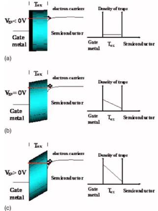
the LFN was dominated by the 1/f⌫共⌫ = 1兲 noise at Vgs= −8 V, but showed degenerated 1/f noise共i.e., the value of ⌫ increases to 2兲 with an increase of the gate bias voltage. We attribute this phenom-enon to the spatial distribution of interfacial trap states within the photo-CVD SiO2 oxide layer, as shown in Fig. 4.28-31 Figure 4a
shows the interfacial trap states for the 1/f⌫noise with exponent⌫ equal to unity are uniformly distributed at Vgs⬍ 0 V. Thus, the 1/f
law is applicable only for the uniform distribution of interface trap states. Interfacial trap states for the 1/f⌫noise with exponent⌫ not equal to 1 are nonuniformly distributed instead, which renders a significant deviation from the 1/f law with an increase of gate bias voltage, as shown in Fig. 4b and c.26-29Therefore, the value of⌫ and the 1/f⌫noise characteristics as a function of Vgsare affected by the interface state distribution in the energy bandgap. Furthermore, Fig. 3b shows the normalized noise power spectra of MOS-HFETs with
Figure 1. The diagram of the MOS-HFET. Rtotal= Rch+ Rs.
Table I. The channel and series resistances in each mode of op-eration for our fabricated MOS-HFETs from experiments.
AlGaN/GaN MOS-HFETs with Photo-CVD SiO2 Gate length = 2m, drain-source distance = 20 m Linear region 共Vds= 3 V, Vgs= 0 V兲 Saturation region 共Vds= 12 V, Vgs= 0 V兲 Cutoff region 共Vgs= −8 V兲 Rch Rs Rch Rs Rch Rs 24⍀ 146⍀ 1124⍀ 146⍀ ⬎104⍀ 146 ⍀
Figure 2.共a兲 Normalized noise spectra of the fabricated MOS-HFETs with different drain-source distance. Here, the devices were all measured by bias-ing in linear region共i.e., Vgs= 0 V, Vds= 3 V兲. 共b兲 Normalized noise power density as functions of drain-source distance at different frequency.
different drain-source distances. These spectra were all measured by biasing the devices at Vgs= 0 V and Vds= 12 V. The measured LFN in the saturation region is practically independent of the drain-source distance, which is understandable given the fact that LFN of our MOS-HFETs in the saturation region is dominated instead by the channel resistance 共underneath the gate region兲, as shown in Table I. Therefore, the effect of drain-source distance on the LFN becomes negligibly small in the saturation region.
In addition, the LFN spectra of the MOS-HFETs with different drain-source distances were also measured by biasing these devices in the cutoff region共not shown兲. It was found that LFN spectra of the fabricated MOS-HFETs could also be fitted reasonably well by the 1/f law up to 10 kHz. In the cutoff region, the channel resistance underneath the gate region is substantially larger than the parasitic series resistance共ungated region兲 共i.e., RchⰇ Rs兲, as shown in Table
I. Thus, the LFN of our MOS-HFETs is also dominated by the channel resistance, which renders the effect of drain-source distance on LFN in the cutoff region insignificant.
The effect of drain-source voltages on LFN.— Figure 5 depicts
the measured noise density of an MOS-HFET as function of Vdsin
different biasing regions. During these measurements, a gate bias of
Vgs= 0 V was applied. As shown in Fig. 5, the normalized noise power density remained at practically the same level in the linear region. However, in the saturation region the normalized noise power density was raised instead in response to an increase in the drain-source voltage. As graphically shown in Fig. 6a, when a
de-vice is biased in the linear region, the entire channel becomes con-ductive and the electrical field distribution in each⌬x remains ap-proximately identical. Thus, the invariant carrier velocity in the conductive channel due to uniform electrical field would result in a lesser current fluctuation and smaller noise power density. When the device is biased in the saturation region, the channel becomes a triangular conductive region, as shown in Fig. 6b. Consequently, different electric fields in⌬x1and⌬x2result in a nonuniform carrier
velocity or current in the channel. Thus, a larger current fluctuation contributes to a higher noise power density. In addition, the variation of the electric field in Fig. 6c is larger than that in Fig. 6b, and this in turn leads to a more severe current fluctuation. Therefore, noise power density increases as the drain-source voltage increases.
Figure 3.共a兲 Normalized noise spectra of the fabricated MOS-HFETs with different gate bias voltages in the saturation region.共b兲 Normalized noise spectra of the fabricated MOS-HFETs with different drain-source distance. These spectra were all measured by biasing the devices in saturation region 共i.e., Vgs= 0 V, Vds= 12 V兲.
Figure 4.共Color online兲 The spatial distribution of interfacial trap states as a function of Vgs in photo-CVD SiO2oxide layer. 共a兲 Vgs⬍ 0 V, 共b兲 Vgs = 0 V,共c兲 Vgs⬎ 0 V.
Figure 5. Normalized noise power density as functions of Vdsfor our MOS-HFET. During these measurements, we applied a gate bias Vgs= 0 V for the MOS-HFETs.
Figure 7 presents normalized noise density as function of Vdsfor
a MOS-HFET biasing in the cutoff region. During these measure-ments, a gate bias of Vgs= −8 V was applied. The noise power density of the devices changed only slightly, which was believed
due to a very large channel resistance when biasing the device in the cutoff region. Thus, we conclude that the LFN of MOS-HFETs is dominated by the channel resistance, as shown in Table I. As a result, the effect of drain-source voltage on LFN again becomes small.
Conclusion
The LFN of AlGaN/GaN MOS-HFETs with a photo-CVD SiO2 gate oxide layer and their dependence on drain-source distance and voltage were investigated. Our results show that the normalized noise power density is inversely proportional to L
⬘
共=Ld-s− Lgate兲 when the device is biased in the linear region. However, the drain-source distance demonstrates no far-reaching effect on the LFN be-havior of MOS-HFETs in the saturation and cutoff region. Further-more, the 1/f⌫noise characteristics and the⌫ value are affected by the interface state distribution in the energy bandgap as the gate bias is varied. The normalized noise power density determined is inde-pendent of the drain-source voltage when the device is biased in the linear region. However, in the saturation region the normalized noise power density increases accordingly as a result of an increase in the drain-source voltage. Finally, the drain-source voltage exerts no ef-fect on the noise power density of devices, as the power remains invariant in the cutoff region.Acknowledgment
This work was supported by the National Science Council under contract no. NSC-93-2215-E-006-010 and NSC-93-2215-E-218-013.
National Cheng Kung University assisted in meeting the publication costs of this article.
References
1. A. Koudymov, G. Simin, M. A. Khan, A. Tarakji, R. Gaska, and M. S. Shur, IEEE
Electron Device Lett., 24, 680共2003兲.
2. C. Q. Chen, J. P. Zhang, V. Adivarahan, A. Koudymov, H. Fatima, G. Simin, J. Yang, and M. A. Khan, Appl. Phys. Lett., 82, 4593共2003兲.
3. H. Hasegawa, T. Inagaki, S. Ootomo, and T. Hashizume, J. Vac. Sci. Technol. B, 21, 1844共2003兲.
4. Y. Nakano, T. Kachi, and T. Jimbo, Appl. Phys. Lett., 83, 4336共2003兲. 5. B. P. Gila, J. Kim, B. Luo, A. Onstine, W. Johnson, F. Ren, C. R. Abernathy, and
S. J. Pearton, Solid-State Electron., 47, 2139共2003兲.
6. D. J. Fu, Y. H. Kwon, T. W. Kang, C. J. Park, K. H. Baek, H. Y. Cho, D. H. Shin, C. H. Lee, and K. S. Chung, Appl. Phys. Lett., 80, 446共2002兲.
7. K. Matocha, R. J. Gutmann, and T. P. Chow, IEEE Trans. Electron Devices, 50, 1200共2003兲.
8. J. W. Johnson, B. Luo, F. Ren, B. P. Gila, W. Krishnamoorthy, C. R. Abernathy, S. J. Pearton, J. I. Chyi, T. E. Nee, C. M. Lee, and C. C. Chuo, Appl. Phys. Lett., 77, 3230共2000兲.
9. M. Hong et al., J. Vac. Sci. Technol. B, 18, 1453共2000兲.
10. B. Gaffey, L. J. Guido, X. W. Wang, and T. P. Ma, IEEE Trans. Electron Devices, 48, 458共2001兲.
11. K. M. Chang, C. C. Cheng, and C. C. Lang, Solid-State Electron., 46, 1399共2002兲. 12. S. J. Chang, Y. K. Su, Y. Z. Chiou, J. R. Chiou, B. R. Huang, C. S. Chang, and J.
F. Chen, J. Electrochem. Soc., 150, C77共2003兲.
13. Y. K. Su, Y. Z. Chiou, S. J. Chang, J. Gong, C. S. Chang, and S. H. Liu, J. Electron.
Mater., 32, 395共2003兲.
14. C. K. Wang, Y. Z. Chiou, S. J. Chang, Y. K. Su, B. R. Huang, T. K. Lin, and S. C. Chen, J. Electron. Mater., 32, 407共2003兲.
15. Y. Z. Chiou, S. J. Chang, Y. K. Su, C. K. Wang, T. K. Lin, and B. R. Huang, IEEE
Trans. Electron Devices, 50, 1748共2003兲.
16. C. K. Wang, T. K. Lin, Y. Z. Chiou, S. J. Chang, Y. K. Su, C. H. Kuo, and T. K. Ko,
Semicond. Sci. Technol., 18, 1033共2003兲.
17. C. K. Wang, S. J. Chang, Y. K. Su, Y. Z. Chiou, T. K. Lin, and B. R. Huang, Phys.
Status Solidi C, 0, 2355共2003兲.
18. C. K. Wang, R. W. Chuang, S. J. Chang, Y. K. Su, S. C. Wei, T. K. Lin, T. K. Ko, Y. Z. Chiou, and J. J. Tang, Mater. Sci. Eng., B, 119, 25共2005兲.
19. C. K. Wang, R. W. Chuang, S. J. Chang, Y. K. Su, S. C. Wei, T. K. Lin, T. K. Ko, Y. Z. Chiou, and J. J. Tang, Mater. Sci. Eng., B, 119, 25共2005兲.
20. C. K. Wang, S. J. Chang, Y. K. Su, Y. Z. Chiou, C. H. Kuo, C. S. Chang, T. K. Lin, T. K. Ko, and J. J. Tang, Jpn. J. Appl. Phys., Part 1, 44, 2458共2005兲. 21. S. L. Rumyantsev, N. Pala, M. S. Shur, M. E. Levinshtein, P. A. Ivanov, and M. A.
Khan, Fluct. Noise Lett., 1, L221共2001兲.
22. S. L. Rumyantsev, N. Pala, M. S. Shur, R. Gaska, M. E. Levinshtein, M. A. Khan, G. Simin, X. Hu, and J. Yang, J. Appl. Phys., 88, 6726共2000兲.
23. S. L. Rumyantsev, N. Pala, M. S. Shur, E. Borovitskaya, A. P. Dmitriev, M. E. Levinshtein, R. Gaska, M. A. Khan, J. Yang, X. Hu, and G. Simin, IEEE Trans.
Electron Devices, 48, 530共2001兲.
24. S. L. Rumyantsev, N. Pala, M. S. Shur, R. Gaska, M. E. Levinshtein, M. A. Khan,
Figure 6.共Color online兲 The conductive channel distribution of the devices biased in共a兲 linear region, 共b兲 saturation region, 共c兲 saturation region with larger Vds.
Figure 7. Normalized noise power density as functions of Vdsfor our MOS-HFETs. During these measurements, we applied a gate bias Vgs= −8 V for the MOS-HFETs.
G. Simin, X. Hu, and J. Yang, J. Appl. Phys., 90, 310共2001兲.
25. Y. C. Lin, S. J. Chang, Y. K. Su, J. F. Chen, S. C. Shei, S. J. Hsu, C. H. Liu, U. H. Liaw, and B. R. Huang, Mater. Sci. Eng., B, 98, 60共2003兲.
26. B. Rong, E. van der Drift, R. J. Reeves, W. G. Sloof, and R. Cheung, J. Vac. Sci.
Technol. B, 19, 2917共2001兲.
27. N. Pala, R. Gaska, S. L. Rumyantsev, M. S. Shur, M. A. Khan, X. Hu, G. Simin,
and J. Yang, Electron. Lett., 36, 268共2000兲.
28. H. H. Chen, S. L. Chen, and J. Gong, Symposium on Semiconductor Modeling & Simulation, 39共1993兲.
29. Z. Celik-Butler and T. Y. Hsiang, Solid-State Electron., 30, 419共1987兲. 30. Z. Celik-Butler and T. Y. Hsiang, IEEE Trans. Electron Devices, 32, 2797共1985兲. 31. G. Reimbold, IEEE Trans. Electron Devices, 31, 1190共1984兲.