國立臺灣大學理學院物理學系 碩士論文
Department of Physics College of Science
National Taiwan University Master Thesis
液晶摻雜硒化鎘奈米柱與量子點製作可調控發光元件 Color-Tunable Light Emitting Device based on the mixture
of CdSe nanorods and dots embedded in Liquid Crystal Cells
陳曉聖
Hsiao-Sheng Chen
指導教授:陳永芳 博士 Advisor: Yang-Fang Chen, Ph.D.
中華民國 98 年 7 月
July, 2009
I
Abstract
A newly designed color-tunable light emitting device based on the mixture of
CdSe nanorods and quantum dots embedded in liquid crystal cells has been developed.
The underlying working principle is derived from a large alignment energy due to the
enhanced anchoring force of liquid crystal molecules through the amplified surface
area of nanorods. After embedded into a liquid crystal cell, nanorods will align along
the orientation of liquid crystal molecules. As the external bias is applied, nanorods
would be driven in the direction according to the orientation of liquid crystal
molecules. The nanorods possess optically anisotropic property, whereas quantum
dots are spherically symmetric. Accordingly, the relative ratio of the emission
intensity between quantum dots and nanorods can be manipulated by an external bias,
and the emission color of the device is therefore tunable. Our work shown here may
pave a new route for the future development of smart optoelectronic devices.
II
摘要
不同於球形的量子點或其他形狀的奈米結構的發光,一維長棒狀
的 奈 米 柱 由 於 其 幾 何 上 的 結 構 , 使 得 其 發 光 具 有 異 相 性
(anisotropy)。然而,卻缺乏將大量的奈米柱排列至同一方向,以及
操控奈米柱方向的方法,因此,我們研究出利用液晶來排列硒化鎘
(CdSe)奈米柱,並且利用半導體的幾何形狀和液晶分子的特性製作出
可調控發光的液晶元件,從我們的研究成果可以發現有趣的現象,對
於奈米柱的應用將更為廣泛。這些研究成果主要包括了:
1.利用液晶操控硒化鎘(CdSe)奈米柱的排列:
由於液晶分子的方向可以順著配向膜配向的方向,因而將單軸分
子作一致性的排列,我們製作液晶 cell 並將硒化鎘(CdSe)的量子點
和奈米柱摻雜於液晶 cell 內。利用光激螢光光譜來比較硒化鎘(CdSe)
量子點和奈米柱的發光偏振行為,我們比較其平行與垂直於配向膜配
向方向之發光強度,我們發現零維量子點其平行和垂直的發光強度沒
有太大的變化,然而,擁有一維結構的奈米柱具有相當強的偏振性
(Polarized PL),除此之外,我們由理論公式去量化奈米柱在液晶
III
cell 裡的排列程度,實驗結果顯示,硒化鎘(CdSe)奈米柱的偏振度
(Polarization ratio)為 0.53,成功的證明利用液晶的分子間作用
力可以將硒化鎘(CdSe)奈米柱作同方向的排列。
2.藉由外加電壓操控硒化鎘(CdSe)奈米柱分子的方向:
液晶(E7)是一種極性分子,當有外加電壓超過臨界電壓時,液晶
分子的長軸會順著外加電場方向,藉由液晶分子的隨外加電壓的特
性,我們可以調控硒化鎘(CdSe)奈米柱分子的方向。同樣地,我們將
硒化鎘(CdSe)量子點和奈米柱摻雜在液晶 cell 裡面,觀察光激螢光
光譜在平行和垂直配向膜配向方向時的發光強度,因為量子點的球形
對稱,當無外加電壓時和加電壓之間的光譜強度維持不變;相反地,
奈米柱因其量子局限效應(Quantum confinement),光譜強度會隨著
電場大小作改變。基於以上的特性,我們設計了一個可調控發光顏色
的液晶元件,相信這樣的成果未來在液晶顯示器與發光二極體將會有
很大的應用。
關鍵詞 : 硒化鎘,量子點,奈米柱,偏振性,液晶元件。
IV
Contents
Chapter 1. Introduction ... 1
1.1 Introduction ... 1
References4 Chapter 2. Theoretical Background...5
2.1.1 Liquid Crystals... 5
2.1.1.1 Calamitic Liquid Crystals... 5
2.1.2 Basic physical properties of Liquid crystals ... 6
2.1.2.1 Orientational order parameter... 6
2.1.2.2 Dielectric anisotropy... 7
2.1.2.3 Refractive Index... 8
2.1.2.4 Elastic constants... 9
2.1.2.5 Viscosity ... 10
2.1.3 Deformation of nematic liquid crystals by an electric field... 11
2. 2.1 Semiconductor nanowires and nanorods ... 16
References ... 19
Chapter 3. Experiment ... 30
3.1 Micro-Photoluminescence ... 30
3.1.1Principles and Applications of Micro-Photoluminescence
V
... 30
3.1.2 The Apparatus for Micro-Photoluminescence Measurement ... 34
3.2 Transmission Electron Microscope (TEM) ... 34
References ... 36
Chapter 4. Color-tunable light emitting device based on the mixture of CdSe nanorods and dots embedded in liquid crystal cells... 40
4.1Introduction... 40
4.2 Experiment ... 41
4.2.1 Sample preparation ... 41
4.2.2 Experimental setup ... 44
4.3 Results and Discussion ... 45
4.4 Summary... 48
References ... 50
Chapter 5 Conclusion ... 56
VI
List of Figures
Figure 2.1 The schematic showing of isotropic liquid phase ... 21
Figure 2.2 The schematic showing of nematic liquid crystal phase .... 21
Figure 2.3 The schematic showing of (a) smectic-A liquid crystal phase, (b) smectic-C liquid crystal phase ... 22
Figure 2.4 The schematic showing of cholesteric liquid crystal phase, where is the director ... 23
Figure 2.5 The schematic showing of smectic-C* liquid crystal phase ...
... 24
Figure 2.6 The schematic showing of (a) splay, (b) twist, and (c) bend deformations in liquid crystal ... 25
Figure 2.7 The schematic showing of three principal viscosity coefficients η
1, η
2,and η
3 ...26
Figure 2.8 Nematic LC under an external bias (a) △ε> 0 (b) △ε< 0 . 26
Figure 2.9 The ionic charges induced by an external field in LC cell. 27
VII
Figure 2.10 The schematic showing of basic geometries of the dielectric reorientation of nematic liquid crystals (△ε>0). On the left hand side, the initial states distinguish by different starting orientations. On the right hand side, the deformed states above the threshold are illustrated... 28
Figure 2.11 Polarized excitation and emission spectra of nanowires. (A) Excitation spectra of a 15-nm-diameter InP nanowire. These spectra were recorded with the polarization of the exciting laser aligned parallel (solid line) and perpendicular (dashed line) to the wire axis. The polarization ratio, ρ, is 0.96. Inset, plot of the polarization ratio as a function of energy. (B) Emission spectra of the same wire as in (A). These spectra were taken with the excitation parallel to the wire, while a polarizer was placed in the detection optics. The polarization ratio of the parallel (solid line) to perpendicular (dashed line) emission is 0.92. The spectra were taken with integration times of 10 s. Inset, plot of the polarization ratio as a function of energy. Reprinted with permission from J. F.
Wang et al., Science 293. 1455(2001) ... 29
Figure 2.12 CL spectra from the nanowire region and substrate region taken for the p(solid spots) and s(open spots) polarization directions. The polarization ratio, ρ, is only 0.5. Reprinted with permission from Appl. Phys. Lett. 88, 153106 (2006) ...
... 29
Figure 3.1 Energy transition in (a) direct and in (b) indirect gap semiconductor between initial states and final states…….37
Figure 3.2 The schematic representation of low temperature photoluminescence (after R. A. Strading and P. C. Klipstein)
...
... 37
VIII
Figure 3.3 Illustration of different processes that can give rise to light emission in semiconductor.
(a) The band to band recombination.
(b)Excitonic recombination.
(c)Free hole-neutral donor recombination.
(d)Free electron recombines with a hole on a neutral acceptor.
(e)Donor-acceptor recombination ... 38
Figure 3.4 The schematic diagram of the experimental setup used in the optical measurement... 39
Figure 3.5 Schematic diagram of TEM ... 39
Figure 4.1 (a) and (b) show transmission electron microscopy (TEM) images of CdSe nanorods and quantum dots, respectively. (c) and (d) show the photoluminescence (PL) spectra of CdSe nanorods and quantum dots, where the maximum PL intensity is at 650 nm (1.9 eV) and 580 nm (2.1 eV) approximately ... 52
Figure 4.2 Schematic shows the structure of the fabricated sample with and without an external bias. The arrow is the rubbing direction. The external field will drive the direction of LC molecules perpendicular to the cell plane, and it will also drive nanorods along the same direction due to the interaction between LC molecules and nanorods... 53
Figure 4.3 The experimental setup for photoluminescence measurement ... 53
Figure 4.4 Dependence of photoluminescence spectra of CdSe nanorods
IX
and quantum dots on the angle of analyzer without an external bias. The inset is the variation of the emission intensity of CdSe nanorods versus analyzer angle ... 54
Figure 4.5 Absorption spectra of CdSe nanorods without an external bias in the case of analyzer parallel (red line) and perpendicular (black line) to the rubbed PI direction... 55
Figure 4.6 Photoluminescence spectra of CdSe nanorods and quantum
dots with an external bias of about 20 V. The inset is the
variation of the emission intensity of CdSe nanorods versus
analyzer angle ... 55
X
List of Tables
Table 4.1 The list of the sample fabrication processes………44
1
Chapter 1 Introduction
1.1 Introduction
One-dimensional nanostructures, such as nanorods, nanowires, and nanotubes,
etc., have become a class of attractive materials as their geometric anisotropy gives
rise to unique physical properties [1-8]. For example, the emission and absorption
spectra arising from one-dimensional semiconducting wires can be highly
anisotropic, and hence serve as an excellent candidate for the application in
polarized optoelectronic devices. On the other hand, liquid crystal (LC) is an
anisotropic fluid, which is thermodynamically between isotropic fluids and
crystalline solid. Liquid crystals (LCs), a promising material, have widely applied
to the LCD [9, 10]. They possess excellent properties such as low-voltage driven,
lightweight and cheapness. Therefore scientists use their in particular characteristics
in many fields for advanced applications. For example, some works have shown
the tunable wavelengths of photonic crystals in semiconductor materials using
infiltrated LCs [11, 12]. The most useful property of LC lies in the fact that its
molecular orientation can be easily controlled via an external bias. On this basis,
numerous applications have been established, among which one prominent case
should be ascribed to the liquid crystal display (LCD). Combining zero and
2
one-dimensional semiconductor nanostructures with the well developed LCD
technology, herein, we propose the feasibility of designing a novel color-tunable
light emitting device. We ingeniously demonstrate a color-tunable emission device
by embedding semiconductor nanorods and quantum dots in a LC cell. The
underlying mechanism is as follows. Nanorods will align along the orientation of
LC molecules due to a large alignment energy caused by the enhanced anchoring
force through amplified surface area in nanomaterials. When the orientation of LC
molecules is altered by an external bias, the reorientation of the nanorods will
follow that of liquid crystal through the minimized elastic energy of interaction via
the electric field. Because the emission of nanorods is strongly anisotropic, and that
of quantum dots is spherically symmetric, i.e. isotropic, we therefore can fine-tune
the ratio of the emission intensity between nanorods and quantum dots. If we
intentionally select nanorods and quantum dots with different emissive wavelengths,
the resulting emission color of this newly designed device could thus be
manipulated. Our result elaborated here should be very useful for the future
development of smart optoelectronic devices.
This thesis is organized in the following manner. In chapter 2, we give an
introduction to theoretical background, including the basic physical principle of
several nematic liquid crystal and one-dimensional semiconductor materials. In
3
chapter 3, the experimental setup and such as micro-PL and TEM are performed. In
chapter 4, we present a detailed description and investigation on our designed
“color-tunable light emitting device”. The polarization of PL and external electrical
experiment are carried out for the further studies. Some interesting results and
discoveries have been obtained from our analyses. Chapter 5 summarizes the
results of this thesis.
4
References
[1]Y. Murakami, E. Einarsson, T. Edamura, S. Maruyama, Phys. Rev. Lett. (2005).
[2] Jianfang Wang, et al. Science 293, 1455 (2001).
[3] H. Y. Chen, Y. C. Yang, H. W. Lin, S. C. Chang, and S. Gwo, OPTICS EXPRESS
16, 13465 (2008).
[4] M. Bashouti, W. Salalha, M. Brumer, E. Zussman, and E. Lifshitz, Chem. Phys.
Chem., 7, 102 (2006).
[5] Mikhail Artemyev, Björn Möller Ulrike Woggon, Nano Lett., 3 (4), 509 (2003).
[6] C. X. Shan, Z. Liu, and S. K. Hark, Phys. Rev. B 74, 153402 (2006).
[7] A. Lan, J. Giblin, V. Protasenko, and M. Kuno, Appl. Phys. Lett. 92, 183110
(2008).
[8] N. Yamamoto, Appl. Phys. Lett. 88, 153106 (2006).
[9] P. G. de Gennes and J. Prost, The Physics of Liquid Crystals (Clarendon, Oxford,
1993).
[10] P. C. Yeh, and C. Gu, Optics of Liquid Crystal Displays (Wiley, New York,
1999).
[11] C. Schuller, F. Klopf, J. P. Reithmaier, M. Kamp, and A. Forchel, Appl. Phys.
Lett. 82, 2767 (2003).
[12] B. Maune, M. Loncar, J. Witzens, M. Hochberg, T. Baehr-Jones, D. Psaltis, A.
Scherer and Yueming Qiu, Appl. Phys. Lett. 85, 360 (2004).
5
Chapter 2
Theoretical Background
2.1.1 Liquid Crystals [1, 2]
2.1.1.1 Calamitic Liquid Crystals
In general, the most usual kind of LCs consists of rod-like molecules with its
molecular axis longer than the other two named calamitic LCs. For example,
considering the nematic LC phase with rod-like molecules, it is found that the long
axes of the molecules prefer to direct along a sure direction when they change from
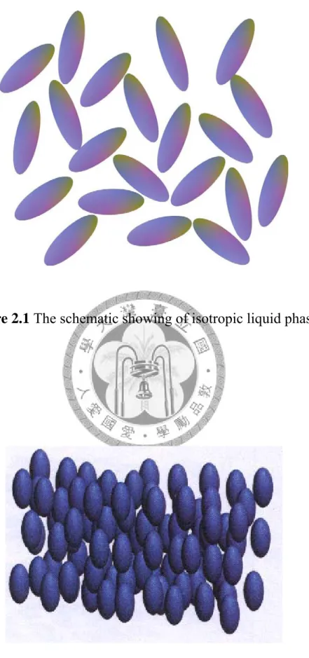
one direction to another. Figure 2.1 and Figure 2.2 show the fundamental difference
between the LC phase and isotropic liquid phase such as water at room temperature.
There are many smectic LC phases in the world. Smectic-A phase and smectic-C
phase are two important cases among those phases. The former describes the director
is parallel to the layer and the latter is at an angle to the layer. Figures 2.3 (a) and (b)
show the difference between smectic-A phase and smectic-C phase.
Another in particular LC phases have the characteristic of chirality, indicating
that those phases do not own inversion symmetry. This leads to the nematic phase and
some of the smectic phases disappear instead of chiral types with various physical
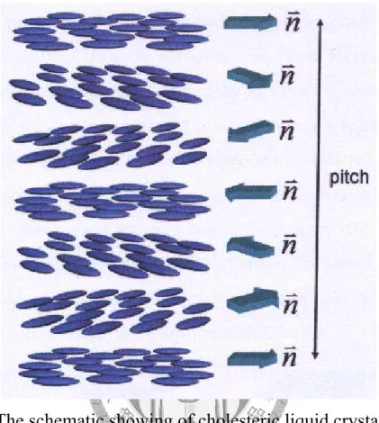
structures. For instance, in a cholesteric phase (chiral nematic phase), the director in
the in-plane layer rotates gradually along a direction perpendicular to the layer as
6
shown in Figure 2.4. The distance called the pitch is defined as the director rotates for
one full revolution also shown in Figure 2.4. The physical structure period should be
indeed half the pitch because of the symmetry between director and .
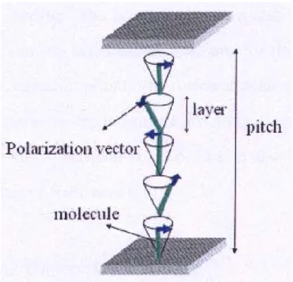
If we replaced the smectic-C phase by the chiral smectic C phase, we can obtain
the phase (smectic-C* phase) whose director keeps a fixed tilt angle in the in-plane
layer. However, the director rotates like a cone from one layer to the next layer as
shown in Figure 2.5. The pitch is the distance for one full revolution around the cone
as illustrated in Figure 2.5.
2.1.2 Basic physical properties of Liquid crystals 2.1.2.1 Orientational order parameter
As described above, the nematic phase of the LCs molecules is rod-like form
with their molecular axis longer than the other two. Therefore, we can define a vector
to state the average preferred orientation of the LCs in the discussed system. We
usually name the vector , the director. Generally speaking, in a homogeneous and
inhomogeneous nematic LCs system, the director is a constant value and depends on
the space position (x, y, z) in the system, respectively. We can define a unit vector to
exhibit the long axis of each molecule, and the director becomes the statistical
average of the unit vectors in a small volume element around the discussed LC
molecules.
7
The orientational order parameter S of a LC can be defined as
, (2.1)
where θ is the angle between the long axis of a LC molecule and the director . For a
perfect parallel alignment, S = 1, while for totally random directions, S = 0. Note that
the nematic phase of LCs usually has an intermediate value of the orientational order
parameter S ranging from 0.4 to 0.6 at low temperatures typically. In addition, the
values of the order parameter S depend on the structure of the molecules and the
temperature dramatically.
2.1.2.2 Dielectric anisotropy
The nematic and smectic LCs are uniaxial symmetry due to the orientational
ordering of the rod-like molecules. Because of the properties of uniaxial symmetry,
the dielectric constants become different in value along the preferred axis (ε∥) and
perpendicular to this axis (ε┴), manifesting the anisotropy of LCs. The dielectric
anisotropy can be defined as
Δε=ε∥ −ε┴, (2.2)
It is noted the dielectric anisotropy Δε is the most important properties when applied
the LCs to LC industry. In order to emphasize the benefit, here we discuss an applied
electric field in nematic LC. The induced dipole moment of the LC molecules is not
parallel to the external electric field due to the anisotropy of LC, except the molecular
8
axis parallel or perpendicular to the electric field. The effect causes a net torque to
align the LC molecules along the direction of the electric field for most rod-like LC
molecules. In the system, the electrostatic energy can be defined as
, (2.3)
where means the electric field vector. is the displacement field vector, which is
independent of the direction of the LCs in a homogeneous surrounding. The director
is parallel to the applied electric field with positive dielectric anisotropy (ε∥> ε┴) of
LCs when minimizing electrostatic energy of the system. In general, the dielectric
anisotropy of the nonpolar LCs with rod-like molecules is positive. However, there is
an excess contribution to the dielectric constant because of the permanent dipole
moment generated in the polar LC molecules. In addition, as result of depending on
the angle between the dipole moment and the molecular axis, the dipole contribution
can result in an increase or a decrease of Δε, finally leading to a negative value of Δε.
The director is perpendicular to the applied electric field with negative dielectric
anisotropy (ε∥< ε┴) of LCs when minimizing electrostatic energy of the system. The
dielectric anisotropy in fact can change from -2εo to 15εo, which also depends on the
temperature strongly.
2.1.2.3 Refractive Index
Nematic LCs often appear as an opaque milky fluid. The scattering of light is due
to the random fluctuation of the refractive index of the sample. The main cause of the
9
scattering leading to the milky appearance is due to the discontinuity of the refractive
index at the domain boundaries. A slab of nematic LC can be obtained with a uniform
alignment of the director. Such a sample exhibits uniaxial optical symmetry with two
principal refractive indices no and ne. The ordinary refractive index no is for light with
electric field polarization perpendicular to the director and the extraordinary refractive
index ne is for light with electric field polarization parallel to the director. The
birefringence (or optical anisotropy) is defined as △n=ne-no. If △n>0, the LC is said
to be positive birefringence, whereas if △n<0, it is said to be negative birefringence.
In classical dielectric theory, the macroscopic refractive index is related to the
molecular polarizability at optical frequencies (~1014 Hz). The existence of the optical
anisotropy is due mainly to the anisotropic molecular structures. Most LCs with
rodlike molecules exhibit positive birefringence ranging from 0.05 to 0.45. The
optical anisotropy plays an important role in changing the polarization state of light in
liquid crystal.
2.1.2.4 Elastic constants
Liquids and solids have the property of elasticity, even LCs possess the curvature
elasticity. If a LC system is disturbed from its equilibrium structure, the magnitude of
restoring torques is decided by the elastic constants of the LC. As compared with
solids, the torques in a LC system present a relatively weak value. The external
10
electric field has been applied to the control of LC reorientation in LC industry. In a
stable LC system, we can obtain the static configuration by balancing the electric
torque and the elastic restoring torque. In a stable LC system, we also can distinguish
into an association of three fundamental deformations: splay, twist, and bend, as
shown in Figure 2.6. The elastic energy in a stable LC system can be determined by a
quadratic function of the curvature strain tensor for an isothermal deformation in an
incompressible fluid. Here we present the elastic energy density of a deformed LC as
follows:
, (2.4)
The symbols of K1, K2, and K3 are the splay, twist, and bend elastic constants,
respectively. As described above such as orientational order parameter and dielectric
anisotropy, the elastic constants strongly depend on temperature.
2.1.2.5 Viscosity
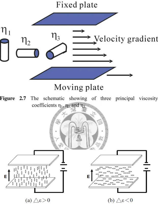
The viscosity of a fluid is defined as the ratio of shearing stress to the rate of
shear. This viscosity causes from the intermolecular forces in the fluid and it presents
an internal resistance to move. In general, the viscosity increases at low temperatures
due to lower molecular kinetic energy. In nematic LCs system, it has been found the
effective viscosity depends on the angle between the director and the direction of flow
and on the direction of the velocity gradient. Here we state three conditions as shown
11
in Figure 2.7. The viscosity coefficient η2 is described as the rod-like molecules are
perpendicular to the velocity gradient, but aligned in the direction of the flow. The
viscosity coefficient η1 is described as the rod-like molecules are parallel to the
velocity gradient, but perpendicular to the direction of the flow. The viscosity
coefficient η3 is described as the rod-like molecules are perpendicular to the velocity
gradient, but perpendicular to the direction of the flow. We can measure those three
viscosity coefficients by oscillating plate viscosimeter. Using this method, we can let
the one bounding plate be fixed while the other one be moved to generate a shear as
shown in Figure 2.7, where the moving plate oscillates at very low frequency. Owing
to the damping of the oscillations via the viscous medium, the viscosity coefficients of
η1, η2, η3 can be evaluated. It is worth noting that the magnitude of the viscosity is not
only affected by attractive intermolecular forces, but also by steric parts such as
length and breadth of the molecules, lateral branches and so on. Here we must
emphasize an important parameter, the rotational viscosity coefficient γ1. It provides a
resistance to the rotational motion of the LC molecules and can be applied to the LC
display. For example, the switching time is approximately proportional to γ1d2 in most
LC display, where d means the distance of the cell gap. In addition, LCs with high
values of dielectric anisotropy Δε often have higher viscosity coefficient.
2.1.3 Deformation of nematic liquid crystals by an electric field
12
Because of very widely important application via using electric field to reorient
the LCs, here we discuss in detail the affection by an electric field. The manifestation
of an electric field results in extra terms in the expression of the following free energy
density:
, (2.5)
We can cancel the first term due to independent of the direction of the director.
Considering the second term, the free energy of the nematic LCs concerned with an
electric field should be a minimum for a definite direction of the director relative to
the field direction due to the dielectric anisotropy Δε. As shown in Figure 2.8, if there
is a nematic LCs system with positive dielectric anisotropy (Δε>0), the stable state
which should minimize the free energy is described by a director parallel to the
external field direction. In contrast, if the nematic LCs system with negative dielectric
anisotropy (Δε<0), the stable state prefers to a director direction perpendicular to the
external field direction. In order to avoid the induced separation of charged impurities
forming electric double layer in LC cell, an alternating voltage across the LC cell. The
electric double layer model is shown in Figure 2.9. In view of an original state that the
direction of the director concerned with external field direction does not satisfy the
condition of minimum free energy, it leads to a sufficiently strong electric field to
generate a torque on the LCs which results in a reorientation of the director. We can
13
obtain a deformed state which owns lower free energy than the original state. The
equilibrium condition to cause a deformed stable state is the balance between the
electric torque and the restoring elastic torque of the LC. In addition, the stable state is
always obtained by the reorientation of director configuration when minimizing the
free energy of the system.
If we think of the electric energy in Equation (2.4), the
distribution of the director all over the system can be evaluated. According to
Equation (2.4), we can derive the critical field strength where the destabilizing electric
torque overcomes the stabilizing restoring elastic torque. Figure 2.10 are illustrated
several field-induced deformations of nematic LCs system. In Figure 2.10 (a), (b), and
(c), three fundamental situations are shown with different initial orientation of the
director. It is noted that the applied electric field is perpendicular to the director in
Figure 2.10 and the dielectric anisotropy Δε is positive so that the director prefers to
align parallel to the external field direction. Figure 2.10 (a) shows the result of a pure
splay deformation for a small director displacement. If having a higher field to the
deformation, we can obtain mainly a splay deformation with a combination of a bend
deformation. The threshold field Eo is given by
, (2.6) where d is the sample thickness.
14
Figure 2.10 (b) shows the result of a pure twist deformation. The threshold field Eo is
given by
, (2.7)
Figure 2.10 (c) shows the result of a small pure bend deformation. If having a higher
field to the deformation, we can obtain mainly a bent deformation with a little splay
deformation. The threshold field Eo is given by
, (2.8)
It must be emphasized that Equations (2.6)-(2.8) are derived under the simplifying
assumptions, where the interaction between the molecules and the surface is strong
and the electric conductivity is neglected here. According to (Uo is threshold
voltage), it indicates that the threshold voltage is independent of the sample thickness.
Similar deformations can be discussed in nematic LCs system with negative dielectric
anisotropy (Δε<0). Then we can obtain the same critical field strength when the
electric field is perpendicular to the situation as shown in Figure 2.10. Figure 2.10 (d)
shows schematically the director alignment in a planar-twisted cell where the twist
angle is 90 degree. The threshold field Eo for a nematic LCs system with positive
dielectric anisotropy (Δε>0) is given by
, (2.9) It should be emphasized here that a decrease of the anchoring energy leads to a
15
decrease of the threshold field Eo. In addition, for a tilted director alignment, there is
no threshold field theoretically. It means that the deformation starts at an infinite
small field strength.
We can derive theoretically the equation of motion of the director (the dynamics
of the field-induced deformations) which presents the balance of the elastic and
viscous forces and the external electric field. Considering a particular case of a pure
twist deformation, it means that the system is not accompanied by a change in
position of the centers of gravity of LC molecules (in contrast to splay and bend
deformations). The equation of motion can be written as:
, (2.10)
where θ is the angle between the local director and the substrates, z is the coordinate
perpendicular to the substrate, t is the time, and γ1 the rotational viscosity. In general,
Equation (2.10) must be solved numerically. However, for some simplifying
assumptions, we can derive the following result for the switching times of the
dielectric reorientation as follows:
, (2.11)
where U is voltage and Uo is the threshold voltage, and
, (2.12)
Equations (2.11) and (2.12) are also valid for bend and splay deformations if small
16
deviations from the initial orientation of the director. Owing to depend on the initial
orientation of the director, in Equation (2.12), different elastic constants can be
replaced K2, for a planar layer K1, for a homeotropic layer K3, and for a planartwisted
layer K1 (K3 – 2K2)/4. Finally, it worth noting that the switching times are mainly
determined by the rotational viscosity γ1 and the sample thickness d from Equations
(2.11) and (2.12). In particular, Δε and the driving voltage are the crucial factors to
affect the rise time.
2. 2.1 Semiconductor nanowires and nanorods [5]
Nanoscale materials have attracted tremendous interest and attention over the
past decade for their vast areas of applications ranging from electronics to
pharmaceuticals.
One-dimensional (1D) nanostructures such as nanowires, nanobelts and
nanotubes have become the focus of intensive research owing to their fascinating
properties, unique applications in macroscopic physics and fabrication of nanoscale
electronic and optoelectronic devices. Semiconductor nanowires have demonstrated
significant potential as fundamental building blocks for electronic and photonic
devices and offer substantial promises for integrated nanosystems. The rectifying
properties of semiconductor nanowires-based electronics demonstrated the versatility
of the nanowires-based electronics device.
17
Quantum confinement effects of the semiconductor nanowires on the other hand,
produce unique optical properties that can be applied to nanophotonic devices.
Notably, the key feature of semiconductor nanowires that has enabled much of their
success has been the growth of materials with reproducible electronic and optical
properties that can be in turn, integrated into functional nanoscale devices.
Consequently, nano-devices based on semiconductor materials such as field-effect
transistors (FETs) [6], lasers [7], light emitting diodes (LEDs) [8] and sensors [9]
have been demonstrated.
Quantum size-confinement plays an important role in determining the energy
levels of 1D nanostructures when its diameter is below the critical Bohr radius. Lu et
al. found that the absorption edge of Si nanowires display significant blue shift as
compared with the indirect bandgap (~1. 1 eV) of bulk silicon [10-12]. They observed
sharp, discrete features in the absorption spectra and relatively strong band-edge
photoluminescence (PL). These different optical features mainly resulted from
quantum-confinement effects and also the variation in growth direction for these Si
nanowires [13]. In contrast to quantum dots, light emitted from nanowires is highly
polarized along the longitudinal axes. One-dimensional nanostructures have thus far
been primarily synthesized by lithography and epitaxial techniques on semiconductor
substrates [14–16]. Free standing nanowires, on the other hand, of many
18
semiconductors have recently been formed by a growth technique using nanosized
liquid droplets of the metal solvent [17–20]. This technique has the advantage of
being able to produce heterogeneous structures along the nanowire, such as p-n
junctions [17] and superlattices [18]. Optical properties of the nanowires formed using
the above technique have been studied by photoluminescence (PL) and absorption
spectroscopy, which showed a blueshift of the peak energy due to the quantum
confinement effect and giant polarization anisotropy in PL and optical absorption.
Those properties provide the potential for new applications of the semiconductor
nanowires. For example, Wang et al. [21] showed a prominent anisotropy in the PL
intensities in the direction parallel and perpendicular to the long axes of an individual,
isolated indium phosphide (InP) nanowires (Figure 2.11), whose polarization ratio is
0.96, but that of numerous InP nanowires grown on a substrate [22] (Figure 2.12), where
some of them were inclined from nomal of substrate, is only 0.5. The magnitude of the
polarization anisotropy could be quantitatively due to the large dielectric constant
contrast between the nanowires and the surrounding environment, as opposed to
quantum mechanical effects such as mixing of valence bands.
19
References
[1] P. J. Collings and M. Hird, R. A. Stradling and P. C. Klipstein, Introduction to
Liquid crystals Chemistry and Physics (Taylor & Francis, 1997).
[2] P. J. Collings, Liquid crystals (Nature’s Delicate Phase of Matter) (Princeton
University Press, 1990).
[3] de Gennes, P. G.; Prost, J. The Physics of Liquid Crystals; Clarendon (Oxford,
1993).
[4] P. C. Yeh, and C. Gu, Optics of Liquid Crystal Displays (Wiley, New York, 1999).
[5] A. A. Balandin and K. L. Wang, Handbook of Semiconductor Nanostructures and
Nanodevices 4 (American Scientific Publishers, Los Angeles, California, USA,
2006).
[6] R. Martel, T Schmidt, H. R. Shea, T. Hertel, and P. Avouris, Appl. Phys. Lett. 73,
2447 (1998).
[7] J.C. Johnson, H. J.Choi, K. R. Knutsen, R D. Schaller, R Yang, and R. J. Saykally,
Nature Mater. 1, 106 (2002).
[8] H. M. Kim, T W. Kang, and K. S. Chung, Adv Mater. 15, 567 (2003).
[9] A. Kolmakov, Y. Zhang, G. Cheng, and M. Moskovits, Adv Mater. 15, 997 (2003).
[10] X. Lu, T. Hanrath, K. P. Johnston, and B. A. Korgel, Nano Lett. 3, 93 (2003).
[11] T. Hanrath and B. A. Korgel, J. Am. Chem. Soc. 124, 1424 (2001).
20
[12] J. D. Holmes, K. P. Johnston, R. C. Doty, and B .A. Korgel, Science 287, 1471
(2000).
[13] M. V Wolkin, J.Jorne, P. M. Fauchet, G. Allan, and C. Deleme, Phys. Rev. Lett.
82, 197 (1999).
[14] Y. Arakawa and H. Sakaki, Appl. Phys. Lett. 40, 939 (1982).
[15] T. Someya, H. Akiyama, and H. Sakaki, Phys. Rev. Lett. 74, 3664 (1995).
[16] P. Ils, M. Michel, A. Forchel, I. Gyuro, M. Klenk, and E. Zielinski, Appl. Phys.
Lett. 64, 496 (1994).
[17] M. S. Gudiksen, L. J. Lauhon, J. Wang, D. C. Smith, and C. M. Lieber, Nature
_London_ 415, 617 (2002).
[18] Y. Wu, R. Fan, and P. Yang, Nano Lett. 2, 83 (2002).
[19] T. Mokari, E. Rothenberg, I. Popov, R. Costi, and U. Bnin, Science 304, 1787
(2004).
[20] J. Goldberger, R. He, Y. Zhang, S. Lee, H. Yan, H-J. Choi, and P. Yang, Nature
(London) 422, 599 (2003).
[21] J. F. Wang, M. S.Gudiksen, X. EDuan, Y. Cui, and C. M. Lieber, Science 293,
1455 (2001).
[22] N. Yamamoto, S. Bhunia and Y. Watanabe, Appl. Phys. Lett. 88, 153106 (2006).
21
Figure 2.1 The schematic showing of isotropic liquid phase.
Figure 2.2 The schematic showing of nematic liquid crystal phase.
22
(a)
(b)
Figure 2.3 The schematic showing of (a) smectic-A liquid crystal phase,
(b) smectic-C liquid crystal phase.
23
Figure 2.4 The schematic showing of cholesteric liquid crystal phase,
where is the director.
24
Figure 2.5 The schematic showing of smectic-C* liquid crystal phase.
25
(a) (b)
(c)
Figure 2.6 The schematic showing of (a) splay, (b) twist, and (c) bend
deformations in liquid crystal.
26
Figure 2.7 The schematic showing of three principal viscosity coefficients η
1, η
2,and η
3.Figure 2.8 Nematic LC under an external bias (a) △ε> 0 (b) △ε< 0.
27
Figure 2.9 The ionic charges induced by an external field in LC cell.
28
Figure 2.10 The schematic showing of basic geometries of the dielectric
reorientation of nematic liquid crystals (
△ε>0). On the left hand side, the
initial states distinguish by different starting orientations. On the right
hand side, the deformed states above the threshold are illustrated.
29
Figure 2.11 Polarized excitation and emission spectraof nanowires. (A) Excitation spectra of a 15-nm-diameter InP nanowire. These spectra were recorded with the polarization of the exciting laser aligned parallel (solid line) and perpendicular (dashed line) to the wire axis. The polarization ratio, ρ, is 0.96. Inset, plot of the polarization ratio as a function of energy.
(B) Emission spectra of the same wire as in (A). These spectra were taken with the excitation parallel to the wire, while a polarizer was placed in the detection optics. The polarization ratio of the parallel (solid line) to perpendicular (dashed line) emission is 0.92. The spectra were taken with integration times of 10 s. Inset, plot of the polarization ratio as a function of energy. Reprinted with permission from J. F. Wang et al., Science 293.
1455(2001).
Figure 2.12 CL spectra from the nanowire region and substrate region taken for the p(solid spots) and s(open spots) polarization directions. The polarization ratio, ρ, is only 0.5. Reprinted with permission from Appl.
Phys. Lett. 88, 153106 (2006).
30
Chapter 3 Experiment
3.1 Micro-Photoluminescence [1]
3.1.1Principles and Applications of Micro-Photoluminescence
For a perfect semiconductor crystal, a light source with photon energy higher
than the band gap of the semiconductor crystal will excite the carriers to their excited
states. As soon as the excitation occurs, all excited electrons and holes will relax to
the bottom of the conduction band and the top of valence band, respectively, and then
the radioactive recombination may occur under the condition of momentum
conservation as shown in Figure 3.1. When the maximum of the valence band and the
minimum of the conduction band occur at the same value of the wave vector k,
transitions are direct and the material is a direct-gap semiconductor (for instance,
GaAs and GaN). For a direct-gap material, the most probable transition is across the
minimum energy gap which is between the most probably filled states at the minimum
of the conduction band and the states most likely to be unoccupied at the maximum of
the valence band. If the band extreme do not occur at the same wave vector k, the
transition is indirect. To hold the condition of momentum conservation in such an
indirect-gap material (for example, Si and Ge), the participation of phonons is
required. Such a process is also called a phonon-assisted process. Therefore, the
31
recombination of electron-hole pairs must be accompanied by the simultaneous
emission of a photon and a phonon. The probability of such a process is significantly
lower as compared with direct transitions. The radioactive recombination that is
caused by the incandescence coming from hot source is called photoluminescence
(PL). As shown in Figure 3.2, for example, if there is a multiplicity of excited states,
only transitions from the lowest excited state can generally be observed at low
temperatures because of rapid thermalization [2]. Figure 3.3 illustrates the process of
photoexcitation, as well as different processes that may cause light emission. If a
photon with its energy higher than the band gap of the sample, an electron in the
valence band will be excited to conduction band and soon dribbles down to the
bottom of conduction band by reaching thermal equilibrium with the lattice, i.e.,
emitting phonons. Figure 3.3(a) is an interband transition. In this case, a direct
recombination between an electron in the conduction band and a hole in the valence
band results in the emission of a photon of energy Eg =hν Although this recombination
occurs from states close to the corresponding band edges, the thermal distribution of
carriers in these states will lead, in general, to a broad emission spectrum. If the
semiconductor is pure, the recombination will be between electrons in the conduction
band and holes in the valence band. As the temperature is sufficiently low (e.g., less
than 25 K for GaAs), an electron and a hole will form a bound state due to the
32
Coulomb interaction. This electron-hole pair is the so-called exciton. The
recombination of an exciton will give rise to sharp-line luminescence with energy of
the band gap minus the binding energy of the exciton. Figure 3.3(b) shows an
excitonic transition. If the semiconductor contains impurities, several new
recombination paths via the impurity states open up. Electrons from the conduction
band may recombine with neutral acceptors which become negatively charged after
recombination (as shown in Fig. 3.3(c)). Neutral donors may recombine with holes in
the valence band, becoming positively charged (as shown in Fig. 3.3(d)). At higher
impurity concentrations electrons bound to donors may recombine directly with holes
bound to acceptors, giving rise to donor–acceptor pair luminescence (as shown in Fig.
3.3(e)). A third category of impurities is isoelectronic impurities, where the impurity
has the same valency as the atom it replaces in the host lattice. The isoelectronic
impurities may bind excitons, which can give luminescence, substantially below the
energy of free excitons. Luminescence studies are, in general, a very powerful method
for obtaining information about impurities, also at low concentrations. It should also
be noted that not all recombination between electrons and holes results in light
emission, since there may also be efficient nonradiative recombination paths. PL is
one of the most useful optical methods for the semiconductor industry [2, 3], with its
powerful and sensitive ability to find impurities and defect levels in silicon and group
33
III-V element semiconductors, which affect materials quality and device performance.
A given impurity produces a set of characteristic spectral features. This fingerprint
identifies the impurity type, and often several different impurities can be seen in a
single PL spectrum. In another use, the full width at half maximum (FWHM) of PL
peak is an indication of sample quality and crystallinity, although such analysis has
not yet become highly quantitative. Besides, PL is sensitive to the strain field inherent
in the semiconductor heterostructures, and can measure the magnitude and the
direction of the strain field. Photoluminescence can also determine the band gaps of
semiconductors. This is very important for binary (AxB1-x) and ternary (AxB1-xC)
alloys whose gaps vary with the compositional parameter x which must be accurately
known for applications. When the relation between gap energy and x is known, the PL
measurement of gap can be inverted to determine x. From this, a two-dimensional
map of alloy composition can be obtained as the exciting laser beam is scanned across
the surface of the sample, which is a useful tool to determine inhomogeneity.
Among the optical characterization methods, PL are probably the best developed
to carry out such spatial scanning, with commercial equipment available. An
interesting PL measurement with the aid of a polarizer can help us study the optical
anisotropy of semiconductor heterostructures. By way of this method, we are able to
investigate the microstructure of the sample and the mechanism of the radioactive
34
recombination of the electrons and the holes in detail.
3.1.2 The Apparatus for Micro-Photoluminescence Measurement
The micro-PL arrangement is the most straightforward measurement in opticalsystem as shown in Figure 3.4. The excitation source can be any laser whose photon
energy is higher than the band gap of the materials to be examined, and whose power
is sufficient to excite an adequate signal. In our measurements, a laser beam with 374
nm is focused into a microscope to be the excitation source. The luminescence from
sample is again focused into the microscope and pass through optical fiber then enters
a TRIAX 320 spectrometer. Finally, a high response H5783 photomultiplier tube is
employed as the detector. The signal from detector switched by SACQ2 sends to
computer. These photons can be generated at continuous powers of watts. Usually,
tens of mW are often adequate to give good signals. The intensity of the Micro-PL
signal apparently depends on the quality of the materials to be examined, the handling
ability of the system, and the sensitivity of the detector.
3.2 Transmission Electron Microscope (TEM)
A main TEM system consists of electron gun, condenser system and objective
lens. The electrons are generated and accelerated to required high energy by electron
gun. A condenser system is set up of different magnetic lenses and apertures makes it
possible to get either a parallel beam (micro probe for TEM) or a convergent beam
35
with selected convergence angles (nano probe for STEM and CBED). Furthermore,
the beam can be scanned (STEM) or tilted (DF-TEM). Most important objective lens
in the microscope since it generates the first intermediate image, the quality of which
determines the resolution of the final image. Images and diffraction pattern can
directly be observed on the viewing screen in the projection chamber or via a TV
camera mounted below the microscope column. Images can be recorded on negative
films, on slow-scan CCD cameras or on imaging plates. Schematic representation of
TEM is shown in Figure 3.5.
36
References
[1] K. J Wu, Master Thesis, N. T. U., Taiwan (2006).;K. C. Chu, Doctoral
dissertation, N.T.U., Taiwan (2005).
[2] R. A. Stradling and P. C. Klipstein, in Growth and Characterisation of
Semiconductors (Hilger, 1990).
[3] S. Perkowitz, in Optical Characterization of Semiconductors: Infrard, Raman, and
Photoluminescence Spectroscopy (Academic Press, 1993).
37
Figure 3.1 Energy transition in (a) direct and in (b) indirect gap semiconductor between initial states and final states.
Figure 3.2 The schematic representation of low temperature
photoluminescence (after R. A. Strading and P. C. Klipstein).
38
Figure 3.3 Illustration of different processes that can give rise to light emission in semiconductor.
(a) The band to band recombination.
(b)Excitonic recombination.
(c)Free hole-neutral donor recombination.
(d)Free electron recombines with a hole on a neutral acceptor.
(e)Donor-acceptor recombination.
39
Figure 3.4 The schematic diagram of the experimental setup used in the optical measurement.
Figure 3.5 Schematic diagram of TEM.
40
Chapter4
Color-tunable light emitting device based on the mixture of CdSe nanorods and dots embedded in liquid crystal cells
4.1 Introduction
One-dimensional nanostructures, such as nanorods, nanowires, and nanotubes,
etc., have become a class of attractive materials as their geometric anisotropy gives
rise to unique physical properties [1-8]. For example, the emission and absorption
spectra arising from one-dimensional semiconducting wires can be highly anisotropic,
and hence serve as an excellent candidate for the application in polarized
optoelectronic devices. On the other hand, liquid crystal (LC) is an anisotropic fluid,
which is thermodynamically between isotropic fluids and crystalline solid. The most
useful property of LC lies in the fact that its molecular orientation can be easily
controlled via an external bias. On this basis, numerous applications have been
established, among which one prominent case should be ascribed to the liquid crystal
display (LCD). Combining zero and one-dimensional semiconductor nanostructures
with the well developed LCD technology, herein, we propose the feasibility of
designing a novel color-tunable light emitting device. We ingeniously demonstrate a
41
color-tunable emission device by embedding semiconductor nanorods and quantum
dots in a LC cell. The underlying mechanism is as follows. Nanorods will align along
the orientation of LC molecules due to a large alignment energy caused by the
enhanced anchoring force through ampled surface area in nanomaterials. When the
orientation of LC molecules is altered by an external bias, the reorientation of the
nanorods will follow that of liquid crystal through the minimized elastic energy of
interaction via the electric field. Because the emission of nanorods is strongly
anisotropic, and that of quantum dots is spherically symmetric, i.e. isotropic, we
therefore can fine-tune the ratio of the emission intensity between nanorods and
quantum dots. If we intentionally select nanorods and quantum dots with different
emissive wavelengths, the resulting emission color of this newly designed device
could thus be manipulated. Our result elaborated here should be very useful for the
future development of smart optoelectronic devices.
4.2 Experiment
4.2.1 Sample preparation
Syntheses of CdSe quantum dots and nanorods have been well documented
[9-12]. In this study, CdSe quantum dots were synthesized by a previously reported
protocol [12], and CdSe nanorods were synthesized according to the reported method,
except for a slight modification regarding the usage of surfactants [13]. In brief, a
42
selenium (Se) injection solution containing 0.073 g of Se was prepared by dissolving
Se powder in 1 ml of tri-n-octyl phosphine. 0.20 g of CdO and 0.71 g of tetradecyl
phosphonic acid (TDPA) were loaded into a 50 ml three-neck flask and heated to 200
°C under Ar flow. After the CdO was completely dissolved, judging by the vanishing
of the brown color of CdO, the Cd-TDPA complex was allowed to cool down to room
temperature. Subsequently, 3.00 g of tri-n-octyl phosphine oxide (TOPO) was added
to the flask, and the temperature was raised to 320 °C to produce an optically clear
solution. At this temperature, the Se injection solution was swiftly injected into the
hot solution. The reaction mixture was maintained at 320 °C for the growth of CdSe
crystals. After 5 min, the temperature was quenched to 40 °C to terminate the reaction.
5 ml of toluene was then introduced to dissolve the reaction mixture, and a brown
precipitate was obtained by adding 5 ml of isopropanol and centrifuged at 3000 rpm
for 5 min. The precipitate was dispersed in toluene for the transmission electron
microscope (TEM) characterization. As the TEM image of CdSe nanorods shown in
Figure 4.1(a), the length and diameter of CdSe nanorods are 25 nm and 7 nm on
average, respectively. The TEM image for the studied CdSe quantum dots is revealed
in Figure 4.1(b), showing that the size of of CdSe quantum dots is about 5 nm. The
corresponding photoluminescence spectra of CdSe nanorods and quantum dots are
shown in Figure 4.1 (c) and (d), respectively.
43
A drawing of the LC cell is depicted in Figure 4.2, in which the top-view and
side-view structures of LC cell, consisting of embedded nanorods and quantum dots,
are presented. The LC cell is composed of two glass substrates with indium tin oxide
(ITO) on the surface, coated by a polyimide (PI, AL21004 (Japan Synthetic Rubber
Corp)) alignment layer. The PI layer, after being spin coated on clean ITO glass
substrate, was then soft baked at 70o C for 110 seconds, hard baked at 240oC for 8
minutes. Subsequently, the PI-coated ITO glass was rubbed to serve as homogeneous
alignment layer for arranging the direction of LC molecules. After preparation of
lower and upper treated substrates, a mixture composed of nematic LC E7 (Merck),
CdSe nanorods and CdSe quantum dots was injected into the cell through a shot
syringe. The distance between lower and upper substrates was about 7μm. Owing to
the capillary force, the cell could be thoroughly filled with LC and CdSe
nanocomposites. The device was then sealed for further measurement. Table 4.1
shows the list of the sample fabrication processes in this work. In this study, the
concentration of CdSe nanorods and quantum dots was about 8.5x1010 cm-3 and 4x10¹⁰
cm-3, respectively. As the top view shown in Figure 2, the nanorods will align with LC
molecules along the rubbing direction due to the surface coupling between LC
molecules and nanorods. When the applied external bias is large enough, the
44
orientation of LC molecules would be forced to align perpendicular to the cell plane,
and the reorientation of nanorods would follow that of LC molecules, as shown in
Figure 2.
Table 4.1 The list of the sample fabrication processes
1. Cut the big ITO glasses into a small one (2x2 cm2).2. Clean the ITO glasses.
3. Spin Coating the ITO glasses with PI layer (AL21004).
4. Bake the ITO glasses after spin coating (70℃ for 110sec & 240℃ for 8 mins).
5. Rub the PI substrate for an unidirection.
7. Compose two substrates (a rubbed PI substrate and a rubbed PI substrate together with AB glue (left and right side).
8. Inject liquid crystal (E7) and CdSe nanocomposites into the LC cell.
9. Seal the composite with AB glue (top and bottom side).
10. Two electric-wires connect with the LC cell.
4.2.2 Experiment setup
Photoluminescence spectra were used to analyze the emission characteristics of
the device containing LC and CdSe nanocomposites. The schematic plot of the
experimental setup is shown in Figure 4.3. A 374 nm laser was used for the pumping
source, which will stimulate the emission of CdSe nanocomposites. The emission
from CdSe nanocomposites passes through the analyzer and depolarizer, and the
signal was detected by a photomultiplier tube (PMT). The analyzer was mounted in
front of the entrance slit of the spectrometer in order to distinguish the orientation of
the polarized electric field. The depolarizer was placed between the entrance slit and
45
the analyzer of the emission signal in order to eliminate the possible error in the
detected polarization due to the measuring equipments. In order to avoid the induced
separation of charged impurities, forming electric double layer in LC cell, we apply an
alternating square wave voltage at 1 kHz frequency across the sample compartment.
4.3 Results and Discussion
Figure 4 shows the polarized behavior of the photoluminescence spectra arising
from CdSe nanorods and quantum dots embedded in LC cell. The maximal
photoluminescence intensities of nanorods and quantum dots are at 580 nm (2.1 eV)
and 650 nm (1.9 eV), respectively. Upon rotating the analyzer angle with respect to
the rubbed PI direction, the emission intensity from CdSe nanorods is then changed
accordingly, while that of CdSe quantum dots remains constant. This result indicates
that CdSe nanorods embedded in the LC cell is well aligned with the LC molecules
along the rubbed direction. It is a consequence of the minimization for the elastic
energy due to interaction between LC molecules and nanorods [19]. The inset in
Figure 4.4 shows the emission intensity of CdSe nanorods as a function of the
analyzer angle, which exhibits a periodic function and follows the cos2θ rule. It is
worth noting that this result is a fully reversible process. In order to confirm the fact
that the observed anisotropic emission indeed arises from the interaction between LC
moles and nanorods, we have fabricated CdSe nanocomposites in a rubbed PI cell
46
without LC infiltration, and the result shows the disappearance of emission
anisotropy.
To gain understanding of the emission anisotropy in a quantitative manner, the
polarization ratio of CdSe nanorods can be calculated by ρ=(I∥-I⊥)/( I∥+I⊥) [14-16],
where I∥and I⊥represent the intensities of emission parallel and perpendicular
to the rubbed PI direction, respectively. The large optical anisotropy could be
rationalized in terms of the differences in dielectric constant between the nanorods and its
surroundings [18]. According to the model developed previously, when the electromagnetic
field is polarized parallel to the nanorod, the electric field inside the nanorod is not reduced.
In contrast, when polarized perpendicular to the cylinder, the electric field amplitude is
attenuated by a factor δ, according to the equation given by
//,
//
i Ee
E (4.1)
2 ,
= δ ,
s s
Ee
Ei
1 ,
1
2 2 2
// 2
2 // 2
//
//
i i
i
E E
E E
I I
I
I i
where Ei is the electric field inside the nanorod, Ee is the excitation field, and ε and εs are the dielectric constant of the nanorod and surrounding, respectively. Consequently, by applying the dielectric constant of CdSe nanorods (bulk ε=10.2) [17] and LC E7 (ε∥=3.02), we then deduce a theoretical value of the polarization ratio of 0.65. In comparison, according to the experimental result shown in Figure 5, the polarization ratio is calculated to be 0.53. The discrepancy between theoretical and experimental values may be attributed to the fact that CdSe nanorods in our study are not an ideal infinite dielectric cylinder as proposed in the theoretical model [18].
(4.2)
(4.3)
47
In order to further examine the dielectric cylinder model for the explanation of
the optical anisotropy of CdSe nanorods, the polarization dependent absorption
spectra were performed. Recorded spectra for the absorbance of CdSe nanorods
parallel and perpendicular to the rubbed PI direction are shown in Figure 4.5. Clearly,
large absorption anisotropy was observed, and the order parameter at 620 nm is
deduced to be 0.54, which is about the same as that measured from
photoluminescence spectra.
Figure 4.6 shows the polarization dependence of the emission spectra of CdSe
nanocomposites embedded in LC cell under an ac square wave voltage of about 20V.
It is found that the emission spectra almost remain the same when the polarization is
parallel and perpendicular to the rubbed PI direction. The inset shows the emission
intensity of CdSe nanorods as a function of analyzer angle. The intensity does not
change with the analyzer angle, but slightly decreases due to fluorescence quenching.
The result implies that when the measurement of the emission intensity is
perpendicular to the cell plane, the emission spectrum is isotropic for the LC cell
under an external bias of 20 V. This behavior can be rationalized as follows. It is well
known that LC director can be driven by an external bias to minimize the electrostatic
energy of the system, and the director of nematic LC (E7) with a positive dielectric
anisotropy will be parallel to the electric field. The anchoring force between nanorods