Characteristics of a sulfur-passivated InGaP/ InGaAs/ GaAs heterostructure
field-effect transistor
Po-Hsien Lai, Ssu-I Fu, Yan-Ying Tsai, and Chih-Hung Yen
Institute of Microelectronics, Department of Electrical Engineering, National Cheng-Kung University, 1 University Road, Tainan, Taiwan 70101, Republic of China
Shiou-Ying Cheng
Department of Electronic Engineering, National Ilan University, No. 1, Sec. 1, Shen-Lung Road, I-Lan, Taiwan 26041, Republic of China
Wen-Chau Liua兲
Institute of Microelectronics, Department of Electrical Engineering, National Cheng-Kung University, 1 University Road, Tainan, Taiwan 70101, Republic of China
共Received 1 April 2005; accepted 5 July 2005; published online 16 August 2005兲
The effect of 共NH4兲2Sx treatment on the device characteristics of an InGaP/ InGaAs/ GaAs heterostructure field-effect transistor are studied and demonstrated. Experimentally, it is found that the sulfur-passivated device shows significant dc characteristics including higher forward voltage, lower leakage current, lower output conductance, and higher voltage gain. The superior microwave performances with flat and wide operating region of drain saturation current are simultaneously obtained. Furthermore, the improved thermal stabilities over wide temperature range of sulfur-passivated devices are attained. Based on these advantages, the studied device with共NH4兲2Sx treatment shows the promise for high-temperature and high-performance microwave applications. © 2005 American Institute of Physics.关DOI: 10.1063/1.2032599兴
Recently, for heterostructure field-effect transistor 共HFET兲 or pseudomorphic high electron mobility transistor, using InGaP to replace AlGaAs as a barrier layer has shown promise for high speed and high-frequency applications.1,2 The advantages of InGaP material include low deep level concentration, low reactivity with carbon and oxygen, and high etching selectivity between InGaP and GaAs.2,3 How-ever, the metal/InGaP Schottky contact generally suffers from the high density of interface states, which results in high recombination velocities and Fermi-level pinning effect.4,5This seriously impedes the limit of scale down and degrades the electronic and optical performances. From the viewpoint of device operation, it is of great concern whether the metal/semiconductor contact can form a high-quality and thermally stable Schottky contact.
In this work, we report a surface passivation using 共NH4兲2Sx solution on an InGaP/ InGaAs/ GaAs HFET. It is known that the sulfur passivation can remove the native ox-ide and suppress the generation of interface traps under a heat treatment.6,7Thus, for promising wide-gap InGaP mate-rial, the surface recombination velocity and surface states are expected to be reduced by sulfur passivation.8,9 This indi-cates that the surface leakage current can be decreased sub-stantially. Furthermore, the sulfur-passivated HFET is ex-pected to show relatively temperature-independent characteristics and high-temperature operation capability.
The studied device was grown by a low-pressure metal-organic chemical vapor deposition system on a 共100兲-oriented semi-insulated 共SI兲 GaAs substrate. The epitaxial layers consisted of a 4000 Å GaAs buffer, a 200 Å AlAs buffer, a 20 Å GaAs spacer, a planar-doped sheet␦1共n+兲=1 ⫻1012cm−2, a 50 Å Al
0.25Ga0.75As spacer, a 150 Å
In0.15Ga0.85As channel, a 20 Å Al0.25Ga0.75As spacer, a planar-doped sheet ␦2共n+兲=4⫻1012cm−2, a 50 Å
n-Al0.25Ga0.75As 共n=3⫻1017cm−3兲 spacer, a 350 Å
n-In0.48Ga0.52P 共n=3⫻1017cm−3兲 barrier, a 300 Å n-GaAs 共n=3⫻1017 cm−3兲 spacer, and a 500 Å n+-GaAs 共n+⭌3 ⫻1018cm−3兲 cap layer. The n-In
0.48Ga0.52P barrier and AlAs buffer layers were employed to provide good Schottky and high breakdown characteristics. It is certainly caused by the suppression of the leakage currents through the gate and buffer leakage paths. After the epitaxial growth, the mesa etching process was used to etch the wafer into substrate to isolate the devices. The drain-source ohmic contacts were formed on n+-GaAs cap layer by alloying evaporated AuGeNi/ Au metals at 435 °C for 3 min. After removing the
n+-GaAs cap and n-GaAs space layers, the studied device A was passivated by dipping into the ammonia-sulfide 关共NH4兲2Sx, 5%兴 solution for 10 min at room temperature. For comparison, another studied device B, prepared by the same process only without the sulfur passivation, was included in this work. Then, the gate Schottky contact was achieved by
evaporating Pt/ Au metal on the undoped
n-In0.49Ga0.51P barrier layer. Finally, materials underneath the gate feeder were completely removed by using wet etch-ing to develop the airbridge gate structure which included multiple piers between the gate pad and active region.10The used gate dimension is 1⫻100m2.
The forward voltage 共VF兲 and the gate leakage current 共IG兲 as a function of temperature are shown in Fig. 1. The VF and IGare measured at the gate current of 1 mA/ mm and the gate-drain voltage of VGD= −22 V, respectively. The inset shows logarithmic value of IGvs VGD of the device A at various temperatures. For device A共B兲, the VF is decreased from 0.861共0.793兲 to 0.603 共0.479兲 V as the temperature is increased from 300 to 510 K. On the other hand, the
corre-a兲Author to whom correspondence should be addressed; electronic mail: [email protected]
APPLIED PHYSICS LETTERS 87, 083502共2005兲
0003-6951/2005/87共8兲/083502/3/$22.50 87, 083502-1 © 2005 American Institute of Physics
sponding IGis increased from 0.6共1兲 to 218共1150兲A / mm. Obviously, the studied device A shows higher VFand smaller
IG than device B among the measured temperature range. The related temperature coefficients of VF and IG 共VF/T andIG/T兲 of device A 共B兲 are −1.23 共−1.50兲 mV/K and 1.04共5.47兲 A / mm K as the temperature is increased from 300 to 510 K, respectively. The negative共positive兲 tempera-ture coefficients of VF共IG兲 are mainly caused by the increase of tunneling component with thermionic emission and partly by the reduction energy gap.11In addition, based on thermi-onic field emission mechanism, the gate-drain current-voltage共I−V兲 characteristics can be expressed as12
I = Is
冉
exp冉
qV
kT
冊
− 1冊
, 共1兲where Is is the reverse saturation current, k the Boltzmann constant, and T the absolute temperature. The Is is deter-mined from a least-square fit to the linear portion of the forward gate-drain I-V curve. For V⬎3 kT/q, the Schottky barrier height 共⌽B兲 can be evaluated from the following relation12: ⌽B= kT q ln
冉
AA*T2 Is冊
, 共2兲where A is the Schottky contact area and A*is the effective Richardson constant. From Eqs.共1兲 and 共2兲, it is known that the reverse saturation currents are affected by the Schottky barrier height and surface state density. Apparently, upon the 共NH4兲2Sxtreatment, the improved Schottky behavior and re-duced surface state density between gate and ohmic elec-trodes of device A are obtained. Thus, the perimeter and intrinsic leakage currents caused by the surface recombina-tion centers of device A are significantly decreased as we expected. This indicates that the 共NH4兲2Sx treatment could offer an effective passivation of the vacancy-related interface traps and suppress their generation resulting from the in-crease of temperature.5–7Therefore, device A shows better thermal stability on VF and IGperformances.
The drain saturation current共IDS兲 as a function of tem-perature under different gate source共VGS兲 are shown in Fig. 2. The typical common source I-V characteristics of the stud-ied device A measured at various temperatures are also
dem-onstrated in the inset. The applied gate-source voltage is
VGS= −0.5 V / step. Due to the improved gate Schottky and better breakdown characteristics by sulfur passivation, the deviations of IDS with increasing temperature are reduced substantially for device A. Moreover, the degraded pinch-off and saturation characteristics associated with significant gate leakage current caused by the increase of temperature are not observed in the studied device A. This is mainly caused by the elimination of native oxides and formation of more stable III–S bonds by sulfur passivation over wide temperature range共300–510 K兲.6–8
The temperature dependences of transconductance共gm兲, output conductance 共gds兲, and voltage gain 共AV兲 are illus-trated in Fig. 3. The biased voltages are fixed at VDS = 3.5共3.5兲 V and VGS= −0.5共−1.0兲 V for device A 共B兲. The
gds is increased slightly from 0.46 共0.49兲 to
0.48共0.51兲 mS/mm for device A 共B兲 as the temperature is increased from 300 to 510 K. On the contrary, the
corre-sponding gm is decreased from 208 共172兲 to
158共125兲 mS/mm. Therefore, the related AV共gm/ gds兲 is de-creased from 450 共350兲 to 330 共243兲 for device A 共B兲. FIG. 1. The forward voltage共VF兲 and gate leakage current 共IG兲 as a function
of temperature. The inset shows the logarithmic value of IGvs gate-drain
voltage共VGD兲 of the device A at various temperatures.
FIG. 2. The drain saturation current共IDS兲 as a function of temperature under different gate-source voltage 共VGS兲. The biased voltage is fixed at VDS = 3.5 V. The inset shows typical common-source I-V characteristics of the device A at various temperatures.
FIG. 3. The transconductance共gm兲, output conductance 共gds兲, and voltage gain共AV兲 as a function of temperature. The biased voltages are fixed at VDS= 3.5共3.5兲 V and VGS= −1.0共−1.5兲 V for device A 共B兲.
083502-2 Lai et al. Appl. Phys. Lett. 87, 083502共2005兲
Clearly, due to the reduction of leakage current associated with good Schottky and better breakdown characteristics, the relatively lower gdsand higher AVof device A are obtained. Even though the ambient temperature is elevated up to 510 K for device A, it is important to notice that the gmand AV at 510 K still maintain 76% and 73.3% of their values at 300 K, respectively. This proves again that the sulfur passivation suppresses the thermally generated interface states as well as the leakage current.6,7 Hence, the sulfur-passivated device still exhibits good amplification performances even at higher operating temperature region.
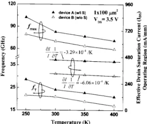
The microwave characteristics are measured by a HP8510B network analyzer in conjunction with Cascade probes at different temperature. The unity current gain cutoff frequency 共fT兲, maximum oscillation frequency 共fmax兲, and effective drain saturation current共IDS兲 operating region as a function of temperature are shown in Fig. 4. The effective drain saturation current operating region is defined as the IDS range where the fT共fmax兲 is larger than 80% of its peak value. Under the bias conditions of VDS= 3.5共3.5兲 V and
VGS= −1.0共−1.5兲 V, the fTof device A共B兲 is decreased from 28.6 共21.6兲 to 20.9 共17.0兲 GHz as the temperature is in-creased from 250 to 400 K. The corresponding fmax is de-creased from 102.4共79.4兲 to 70.8 共59.3兲 GHz. Moreover, the effective IDS operating regions of the device A共B兲 are 455 共330兲, 445 共320兲, and 440 共310兲mA/mm at T=300, 350, and 400 K, respectively. Obviously, the studied device A shows
good microwave characteristics and low degradation rate 共I / I , 1 /T兲 in IDS operating regions共−3.29⫻10−4/ K兲. It is attributed to the increase of thermally stable group-III ele-ments without dangling bonds on the InGaP surface by the sulfur passivation.6,7,13 This can suppress the gate leakage current and improve rf performances. Therefore, the sulfur-passivated device provides the promise for high-frequency applications.
The temperature-dependent characteristics of a sulfur-passivated InGaP/ InGaAs/ GaAs HFET are studied and demonstrated. Experimentally, for a used 1⫻100m2-gated dimension, the sulfur-passivated device exhibits good perfor-mances including higher forward voltage of 0.861共0.603兲 V, lower gate leakage current of 0.6共218兲A / mm at VGD= −22 V, lower output conductance of 0.46共0.48兲 mS/mm, and higher voltage gain of 450 共330兲 at 300 共510兲 K. The corresponding fT and fmax are 28.6 共20.9兲 and 102.4 共70.8兲 GHz at 250 共400兲 K, respectively. Moreover, the relatively lower temperature coefficients of device performances over wide temperature range共300–510 K兲 are observed.
Part of this work was supported by the National Science Council of the Republic of China under Contract Nos. NSC-93-2215-E-006-002 and 93-2215-E-197-004. The authors are also grateful to National Nano Device Laboratories 共NDL兲 for rf measurements.
1W. C. Hsu, H. M. Shieh, M. J. Kao, R. T. Hsu, and Y. H. Wu, IEEE Trans. Electron Devices ED-40, 1630共1993兲.
2H. M. Chuang, S. Y. Cheng, P. H. Lai, X. D. Liao, C. Y. Chen, C. H. Yen, R. C. Liu, and W. C. Liu, Semicond. Sci. Technol. 19, 87共2004兲. 3P. H. Lai, H. M. Chuang, S. F. Tsai, C. I. Kao, H. R. Chen, C. Y. Chen, and
W. C. Liu, Semicond. Sci. Technol. 19, 864共2004兲.
4H. Oigawa, J. Fan, Y. Nannichi, H. Sugahara, and M. Oshima, Jpn. J. Appl. Phys., Part 2 30, L322共1991兲.
5Y. K. Kim, S. Kim, J. M. Seo, S. Ahn, K. J. Kim, T. K. Kang, and B. Kim, J. Vac. Sci. Technol. A 15, 1124共1997兲.
6S. D. Kwon, C. H. Kim, H. K. Kwon, B. D. Choe, and H. Lim, J. Appl. Phys. 77, 2202共1995兲.
7C. R. Moon, B. D. Choe, S. D. Kwon, and H. Lim, J. Appl. Phys. 81, 2904 共1997兲.
8S. J. Pearton, F. Ren, W. S. Hobson, C. R. Abernathy, and U. K. Chakra-barti, J. Vac. Sci. Technol. A 12, 142共1994兲.
9C. T. Lee, M. H. Lan, and C. D. Tsai, Solid-State Electron. 41, 1715 共1997兲.
10W. S. Lour and C. Y. Lia, Semicond. Sci. Technol. 13, 796共1998兲. 11W. C. Liu, W. L. Chang, W. S. Lour, S. Y. Cheng, Y. H. Shie, J. Y. Chen,
W. C. Wang, and H. J. Pan, IEEE Electron Device Lett. EDL-20, 274 共1999兲.
12S. M. Sze, Physics of Semiconductor Devices, 2nd ed.共Wiley, New York, 1981兲.
13R. Hakimi and M. C. Amann, Semicond. Sci. Technol. 12, 778共1997兲. FIG. 4. The unity current gain cutoff frequency共fT兲, maximum oscillation
frequency共fmax兲, and effective drain saturation current 共IDS兲 operating re-gion as a function of temperature. The biased voltages are fixed at VDS = 3.5共3.5兲 V and VGS= −1.0共−1.5兲 V for device A 共B兲.
083502-3 Lai et al. Appl. Phys. Lett. 87, 083502共2005兲