Chapter 2
Design and Analysis of 1x(2N+1) MMI Power Splitter Based on SOQ Waveguide
In this chapter, we use the beam propagation method (BPM) to stimulate the size of 1x(2N+1) MMI power splitters based on Sol-Gel waveguide. As mentioned in Chapter 1, the development of integrated optical devices has become the future trend. We design a symmetric 1x(2N+1) multimode interference (MMI) power splitters based on Er
3+doped Sol-Gel waveguide in this chapter. This chapter is organized as
following: Section 2-1 introduces the technique of Sol-Gel waveguide and
the advantages of the Sol Gel waveguide. The mathematic formulation of
beam propagation method (BPM) are also briefly derived and discussed in
Section 2-1. Section 2-2 introduces the technique of MMI devices. The
advantages of MMI devices applied to integrated optics are presented and
various functions of the MMI structure are also presented. The mathematic
formulation of MMI structure is also briefly described in Section 2-2. The
characteristics of our designed MMI optical splitters based on Er
3+doped
Sol-Gel waveguide by computer-aided beam propagation method software based on BeamPROP_CAD are presented in Section 2-3. We also give the summary of our designed 1x(2N+1) MMI optical splitters based on Er
3+doped Sol-Gel waveguide in the final Section 2-4.
2-1 Introduction of the Technique of Sol-Gel Waveguide
Interest in the sol-gel processing of inorganic ceramic and glass materials began as early as the mid-1800s with Ebelman [12], and Graham's [13] studies on silica gels. These early investigators observed that the hydrolysis of tetraethyl orthosilicate (TEOS), Si(OC
2H
5), under acidic conditions yielded SiO
2in the form of a glass-like material. Also Fibers could be drawn from the viscous gel. It was not until 1930 that Schott exploited sol gel technique to produce optical coatings, while the importance of solution-deposited films for planar waveguides was outlined by researchers at Bell Labs [14] in 1972. Most of the activity has been concerned with the development of waveguides based on silica glass films, both for their low loss and for their compatibility with optical fiber.
Recently photonics devices based on sol gel technique have developed into
important components for integrated photonics device. Its advantages are low-cost route, versatility in fabrication, low-loss. Several sol gel devices have been reported, such as optical-fiber sensor [15], optical waveguide [16], dye laser [17], biosensor [18].
2-1-1 Mathematic Formulation of Beam Propagation Method
In this chapter, we design and simulate the optical Sol-gel silica
waveguide devices based on beam propagation method [19] which is the
most commonly used propagation technique for the modeling of integrated
photonic devices and fiber-optic devices [20-21]. It is necessary to
modeling and optimizing the parameters such as geometry shape, size,
polarization state, material data, input wavelength, and output field profile,
etc. Because it can avoid the material wasting, save testing time of
experiments, and improve realization of the device before we fabricate the
device. Besides, we can get some information to modify the device for
superior performance according to analyzing the simulation result. The
BPM is an approach, which is approximating the exact wave equation for
monochromatic waves, and can solve the resulting equations numerically.
Procedures of Finite difference BPM (FD-BPM) are standard numerical technique [22]. The optical field within one propagation step is calculated along the longitudinal coordinate z to
z+ Δ
z. The electric and magnetic field derived from the Maxwell’s equation can be represented as [23 ]
t E B
∂
− ∂
=
×
∇ K K
(2-1-1)
t J D
H ∂
+ ∂
=
×
∇
K K
K (2-1-2)
= 0
⋅
∇ D K
(2-1-3)
= 0
⋅
∇ B K
(2-1-4) where E K
is the intensity of the electric field, B K
is the flux density of the magnetic field, D K
is flux density of the electric field, H K
is intensity of magnetic field and J K
is electric current density. In a source-free Maxwell’s equation
JK = 0
, the wave equation under scalar field assumption can be written in the form of the well-known Helmholtz equation for monochromatic waves [24]
( , , )
20
2 2 2 2 2
2
+ Φ =
∂ Φ + ∂
∂ Φ + ∂
∂ Φ
∂
k x y zz y
x
(2-1-5)
The scalar electric field has been written as
E(
x,
y,
z,
t) = Φ (
x,
y,
x)
e−iωt,
and the notation
k= ω ε
0μ
0is for the spatially dependent wavenumber,
with
λ π 2
0
=
k
is the wavenumber in free space and
n(
x,
y,
z) is the refractive index distribution. In typical guided-wave problems the most rapid variation in the field Φ is the phase variation due to propagation along the guiding axis, and assuming that axis is predominantly along the z direction. Then, Φ (
x,
y,
z) is expressed as
) exp(
) , , ( ) , ,
(
x y z=
u x y z ikzΦ (2-1-6) where
k=
k0n, which is referred to as the reference wavenumber, represents the average variation of Φ (
x,
y,
z) and n is reference refractive index. Then, we obtain the following equation for the slowly varying field:
0 ) (
2
2 2 22 2 2 2
2
+ − =
∂ + ∂
∂ + ∂
∂ + ∂
∂
∂
k k uy u x
u z
k u z i
u
(2-1-7)
Assumption the variation of u with z is sufficiently slow so that the first term above can be neglected with respect to the second. The above equation is reduces to:
⎟⎟ ⎠
⎜⎜ ⎞
⎝
⎛ + −
∂ + ∂
∂
= ∂
∂
∂
k k uy u x
u k i z
u
( )
2
2 2 2 2 2 2
(2-1-8)
The equation (2-1-8) is the basic formulate for BPM simulations. The
boundary condition we use is the so-called transparent boundary condition
(TBC) [25]. BPM included Polarization effects by recognizing that the
electric field E is a vector, and starting the derivation from the vector wave equation rather than the scalar Helmholtz equation [26]. The equation (2-1-8) is formulated in terms of the transverse components of the field ( E
xand E
y). The equations for the corresponding slowly varying fields ( u
xand u
y) can be expressed as [26]
y xy x xx
x
A u A u
z
u = +
∂
∂ (2-1-9)
y yy x yx
y
A u A u
z
u = +
∂
∂ (2-1-10)
, where
} ) (
)]
1 ( [ 2 {
2 2 2
2 2
2 x x x
x
xx
u k k u
u y x n n x k u i
A + −
∂ + ∂
∂
∂
∂
= ∂ (2-1-11)
} ) (
)]
1 ( [ 2 {
2 2 2
2 2
y y
y y
yy
n u k k u
y n u y
x k u i
A + −
∂
∂
∂ + ∂
∂
= ∂ (2-1-12)
} )]
1 ( [ 2 {
2 2
2 x x
x
yx
u
x u y
x n n y k u i
A ∂ ∂
− ∂
∂
∂
∂
= ∂ (2-1-13)
} )]
1 ( [ 2 {
2 2
2 y y
x
xx
u
y u x
y n n x k u i
A ∂ ∂
− ∂
∂
∂
∂
= ∂ (2-1-14)
The above equations are generally referred to as describing a full-vectorial
BPM.
2-1-2 Erbium doped waveguide amplifier based sol gel method
EDWAs have been demonstrated using a variety of materials systems and fabrication techniques. EDWAs based on ion exchange waveguides in erbium-doped phosphate glass monoliths are perhaps the most advanced [27]. Glass waveguides offer important advantages in terms of integration possibilities. The silica-on-quartz system is well established for passive devices such as arrayed waveguide gratings and splitters. And it also provides good mechanical properties, well-developed processes, and excellent physical and chemical robustness. Consequently, most reported EDWAs have employed other glass types, for example using deposited phosphate [28] and soda-lime [29] waveguides. However, there are drawbacks to these glass types as well, such as low chemical and thermal stability, lack of suitability of refractive indices. But a system that gives high gain levels per unit length remains a very attractive prospect for EDWA implementation.
For photonic devices based on silicate glasses, two deposition methods
have been dominant: flame hydrolysis deposition (FHD), and plasma-enhanced chemical vapor deposition (PECVD). EDWAs have been reported based on both FHD [30] and PECVD [31]. However, the sol-gel process, offers an alternative approach. The sol-gel technique has been extensively studied as an alternative glass deposition method for photonics.
Typically, in this method, metallorganic precursors such as
tetra-ethyl-orthosilicate (TEOS) in an alcohol solution are mixed with
catalyzed water and undergo hydrolysis and condensation reactions. A
viscous suspension of oxide particles on a nanometer scale is formed which
can be spun on a substrate, whereupon the solvent evaporates rapidly. This
increases the particle concentration, and thus the reaction rates, causing the
sol to be a stiff gel. Further heat treatment is then needed to drive off
remaining solvent, to remove residual organic groups, and to collapse the
pores. Based on this approach, channel waveguides and optical splitters
have been developed with low loss. Sol-gel is attractive for active
waveguide fabrication partially because of the ease with which dopants can
be added. Metalalkoxides are commercially available for a wide variety of
metal species, including erbium and other rare earths as well as desirable
co-dopants such as aluminum, and although these compounds may have
widely differing solubility and reaction rates, a process can often be developed by which they may be combined in a homogeneous sol. Dopants can also often be added as inorganic salts. Although the solid thus formed requires heat treatment to remove pores, these pores are on a nanometer scale and so can be collapsed without allowing significant restructuring of the glass by diffusion. Consequently, a fundamental possibility arises: that sol-gel may allow the fabrication of a stable inorganic glass, homogeneous at a molecular scale, which is inaccessible by other techniques.
High-concentration doping of Er in silica is then a possible application.
Relative gain in sol-gel based Er-doped waveguides was first achieved by the use of a strip loaded format [32], but high coupling and background propagation losses prevented net fiber-to-fiber gain from being reached.
Relative gain was also achieved in Er-doped hybrid inorganic–organic
sol-gel waveguides, by minimizing OH content [33]. It has generally been
assumed that the ability of Er-doped sol-gel films to sustain high inversion
at high doping levels results from a lower level of erbium clustering and
that this in turn results from the formation of a uniform molecular structure
in the gel which is retained in the final glass. However, previous studies
have not clearly demonstrated this cause.
2-2 Introduction of the Technique of MMI Structure
The operation and theory of MMI devices is based on self-imaging effect in the multimode waveguide. Self-imaging is that an input field profile is reproduced in single or multiple images at period in the propagation direction of the guided multimode waveguide [34]. Bryngdahl first proposed the possibility of achieving self-imaging in uniform index slab waveguide [35]. Ulrich made a theoretical and experimental research of the self-imaging properties of dielectric waveguide [36-37].
MMI devices have recently developed into key components for
integrated optical circuits. Their advantages, such as stable splitting ratio,
compact size, low loss, large optical bandwidth, insensitivity to polarization,
good fabrication tolerances [38], and simplicity of production have led to
their rapid integration in more complex integrated optical circuits. Several
MMI devices have been reported, such as 3dB couplers [39], power
splitters [40-41], polarization splitter [42], laser diode [43], electro-optical
switch [44], Mach-Zehnder interferometers [45], ring laser [46], and
wavelength division multiplexer [47] .
2-2-1 Mathematic Formulation of MMI Structure
In this section, we design the 1x(2N+1) power splitter on sol-gel glass waveguide based on beam propagation method which is a particular approach for the modeling and simulation of electromagnetic wave propagation in guided-wave optoelectronic and fiber-optic devices. The beam propagation method is a mathematical method and a propagation technique for the numerical simulation of general optical integrated circuits [48].
The theory describes the light propagation in the MMI section and characteristics of the MMI structure includes the generation of the images.
We do not calculate the absorption of material, extinction ratio, or back reflections at the input and output of access waveguides.
The simulation results of 1x(2N+1) MMI optical splitters based on Sol-Gel Er
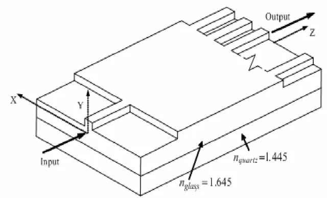
3+ waveguide by computer-aided beam propagation method software based on BeamPROP_CAD for input light wavelength at 1.55μm are shown in this section. The structure of our designed 1x(2N+1) MMI optical splitters is shown as Fig. 2-3.
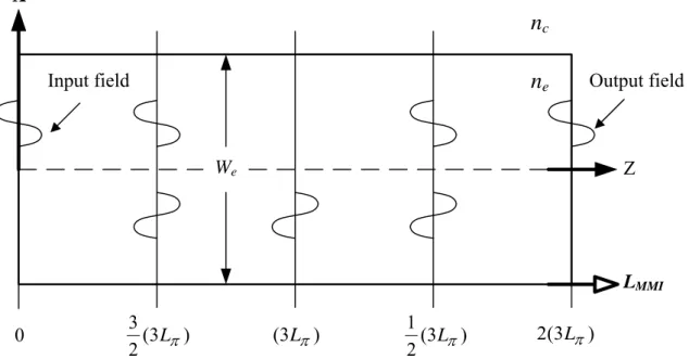
In a homogeneous multimode waveguide of width W
ea beat length of
the two lowest-order modes is defined as [34]
λ β
β π
π
3
4
21 0
e eW
L
≈
n= − (2-2-1) where β
0and β
1are the propagation constants of the fundamental mode and first order modes in the step-index multimode waveguide, respectively, λ is the free space wavelength, n
eis the slab effective index at the guiding region, and
Weis the effective width of the fundamental mode of the multimode guiding waveguide. Note that
W is slightly larger than e WMMI. Both
neand
Weare polarization-dependent. Generally, the beat length corresponding to TE and TM polarizations are not equal for arbitrary waveguide structure. For 1xN optical splitter, the length of multimode can be expressed as [34 ]
( )
λ π
λ
σ3 ) (
2 5 . 2 0 2 2
⎥ ⎥
⎦
⎤
⎢ ⎢
⎣
⎡ ⎟⎟ −
⎠
⎜⎜ ⎞
⎝ + ⎛
=
− c e e
c MMI
e
MMI
n n n
W n n
L
(2-2-2)
, where σ = 0 for TE wave, and σ = 1 for TM wave.
The excess loss of the 1xN optical splitter is defined as [49]
in i i out
P Loss P
Excess
10 log Σ
_−
=
(2-2-3), where
Pout_iis the intensity of each output port and P
inis the intensity
of the input port. The uniformity (or imbalance) of the 1xN optical splitter
is defined as [ ]
Uniformity
= P
InsertionLoss_ max− P
InsetionLoss_ min(2-2-4)
, where P
out−maxand P
out−minare the maximum and minimum intensity of output ports, respectively.
2-3 Simulation Results of 1x(2N+1) MMI Power Splitters Based on Sol-Gel Er
3+Doped Waveguide
Based on Esq. (2-1-2-1) and (2-1-2-2), we calculate and simulate the single mode waveguide width for sol gel glass. We design the rib waveguide with width w =3μm, rib height H =2.56μm and slab height
h =1.69μm for providing single mode operation in input and output
waveguides. The length of input single mode waveguide L
inis 100μm and
the same length with output single mode waveguide L
out. The sol gel glass
refractive index we use is 1.645. And the substrate we use is quartz, its
refractive index is 1.445.
2-3-1 1 x 3 MMI Power Splitter based on Sol-Gel glass waveguide
The input single mode rib waveguide is located at the center of the start wall of the MMI section, and the three output single mode rib waveguides are located at
WMMI/ 3 , 0, and −
WMMI/ 3 in the X axes, respectively, on the end wall of the MMI section. We design the multimode waveguide of a 1x3 MMI power splitter as 18μm. First, we simulate the length characteristics of MMI waveguide. Fig. 2-4 shows the length variation of the multimode waveguide of a 1x3 power splitter. The excess loss of the device is less than 0.5dB at L
MMI=487 to 497μm for TE and TM mode. The uniformity is almost flat and less than 0.01dB at L
MMI=483~494μm for TE and TM mode. The minimum excess loss of the device is about 0.176dB for TE mode at
LMMI=491.3μm, and is 0.153dB for TM mode at
LMMI=486.1μm.
For low polarization dependent loss (PDL), we design the length and width
of multimode waveguide of MMI power splitter as 493.3μm and 18μm,
respectively. In the following, we analyze the variation of geometry size
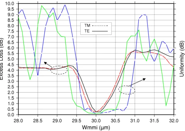
and launch wavelength for this 1x3 MMI power splitter. Fig. 2-5 shows the
width variation of multimode interference waveguide. When the width of
MMI waveguide is between 17.7μm and 18.3μm, we can see that excess
loss is less than 1dB and uniformity is less than 0.6dB. The mean value of uniformity is about 0.4dB for TE mode and is about 0.6dB for TM mode between 17.5μm and 18.5μm. Fig. 2-6 shows the response of input light wavelength of this 1x3 MMI power splitter. The excess loss of this 1x3 MMI optical splitter is less than 2.6dB and the uniformity is less than 0.72dB at input wavelength between 1.5μm and 1.6μm for TE and TM mode. In Fig. 2-7, we analyze the variation of rib part (the etched depth
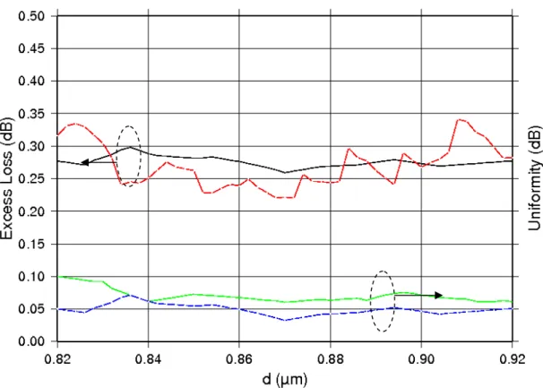
d) on our designed device. When the etched depth is between 0.82μm to 0.92μm, excess loss of the device is less than 0.28dB and uniformity of the device is less than 0.07dB. The mean value of excess loss of the device for TE mode and TM mode is about 0.21dB and 0.20dB, respectively. The mean value of uniformity of the device about TE mode and TM mode is 0.048dB and 0.05dB, respectively.
2-3-2 1 x 5 MMI Power Splitter based on Sol-Gel glass waveguide
The input single mode rib waveguide is located at the center of the start
wall of the MMI section, and the five output single mode rib waveguides
are located at 2 W
MMI/ 5 , W
MMI/ 5 , 0, − W
MMI/ 5 and − 2 W
MMI/ 5 in the X
axes, respectively, on the end wall of the MMI section. We design the
multimode waveguide of a 1x5 MMI optical splitter as 30μm. First, we simulate the length characteristics of MMI waveguide. Fig. 2-8 shows the length variation of the multimode waveguide of the 1x5 power splitter. The excess loss of the device is less than 1.0dB at
LMMI= 1193.7~1209.6μm for TE and TM mode. The uniformity is almost flat and less than 0.5dB at
LMMI
=1190~1210μm for TE and TM mode. The minimum excess loss of
the device is 0.230dB for TE mode at
LMMI=1203μm, and is 0.200dB for
TM mode at
LMMI=1203μm. For PDL, we design the length and width of
multimode waveguide of the 1x5 MMI optical splitter as 1203m and 30μm,
respectively. In the following, we analyze the variation of geometry size
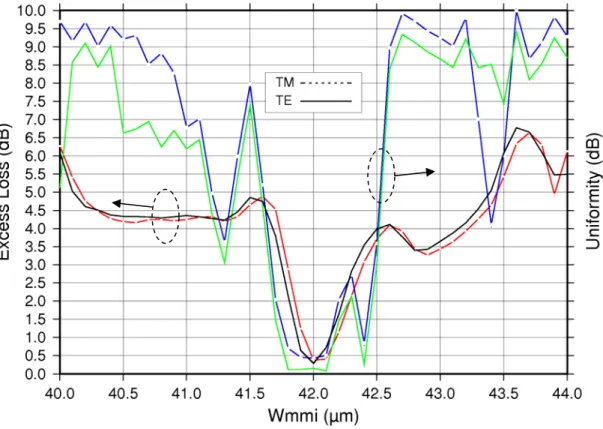
and launch wavelength for the 1x5 MMI optical splitter. Fig. 2-9 shows the
width variation of multimode interference waveguide. When the width of
MMI waveguide is between 29.9μm and 30.3μm, we can see that excess
loss is less than 1.0dB and uniformity is less than 0.28dB. The mean value
of uniformity is about 0.46dB for TE mode and is about 0.38dB for TM
mode between 29.7 and 30.58. Fig. 2-10 shows the response of input light
wavelength of 1x5 MMI optical splitter. The excess loss of this 1x5 MMI
optical splitter is less than 1.5dB between 1,53μm and 1.56μm, the
uniformity is less than 1.0dB at input wavelength between 1.52μm and
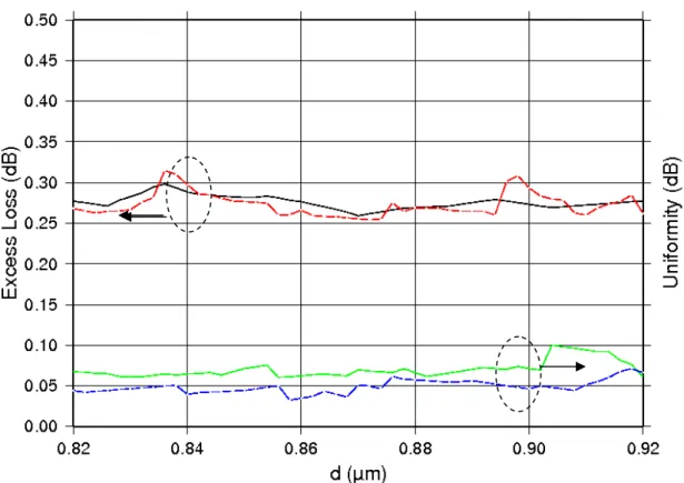
1.58μm for TE and TM mode. In Fig. 2-11 we analyze the variation of rib
part (the etched depth
d) on our designed device. When the etched depth
is between 0.82μm to 0.92m, excess loss of the device is less than 0.34dB and uniformity of the device is less than 0.10B. The mean value of excess loss of the device for TE mode and TM mode is about 0.27B and 0.25B, respectively. The mean value of uniformity of the device about TE mode and TM mode is 0.07B and 0.05dB, respectively.
2-3-3 1 x 7 MMI Optical Splitter based on Sol-Gel glass waveguide
The input single mode rib waveguide is located at the center of the start wall of the MMI section, and the five output single mode rib waveguides are located at 3 W
MMI/ 7 , 2 W
MMI/ 7 , W
MMI/ 7 , 0, − W
MMI/ 7 , − 2 W
MMI/ 7 and
7 / 3 W
MMI− in the X axes, respectively, on the end wall of the MMI section.
We design the multimode waveguide of a 1x7 MMI power splitter as 42μm.
First, we simulate the length characteristics of MMI waveguide. Fig. 2-12 shows the length variation of the multimode waveguide of the 1x7 power splitter. The excess loss of the device is less than 2.0dB at
LMMI
=2747.3~2786.4μm for TE and TM mode. The uniformity is almost flat and less than 1.5dB at L
MMI=2757.7~2784.8μm for TE and TM mode.
The minimum excess loss of the device is 0.276dB for TE mode at
LMMI
=2763μm, and is 0.261dB for TM mode at
LMMI=2763μm. For low
PDL, we design the length and width of multimode waveguide of the 1x7
MMI optical splitter as 2763μm and 42μm, respectively. In the following,
we analyze the variation of geometry size and launch wavelength for the
1x7 MMI optical splitter. Fig. 2-13 shows the width variation of multimode
interference waveguide. When the width of MMI waveguide is between
41.82μm and 42.41μm, we can see that excess loss is less than 2.0dB and
uniformity is less than 2.0dB. The mean value of uniformity is about
0.30dB for TE mode and is about 0.50dB for TM mode between 41.7μm
and 42.2μm. Fig. 2-14 shows the response of input light wavelength of the
1x7 MMI power splitter. The excess loss of this 1x7 MMI optical splitter is
less than 1.5dB between 1.543μm and 1.555μm and the uniformity is less
than 0.88dB at input wavelength between 1.5μm and 1.6μm for TE and TM
mode. In Fig. 2-15, we analyze the variation of rib part (the etched depth
d) on our designed device. When the etched depth is between 0.82μm to
0.92μm, excess loss of the device is less than 0.35dB and uniformity of the
device is less than 0.10dB. The mean value of excess loss of the device for
TE mode and TM mode is about 0.26dB and 0.25dB, respectively. The
mean value of uniformity of the device about TE mode and TM mode is
0.07dB and 0.05dB, respectively.
2-3-4 1 x 9 MMI Optical Splitter based on Sol-Gel glass waveguide
The input single mode rib waveguide is located at the center of the start wall of the MMI section, and the five output single mode rib waveguides are located at 4 W
MMI/ 9 , 3 W
MMI/ 9 , 2 W
MMI/ 9 , W
MMI/ 9 , 0, − W
MMI/ 9 ,
9 / 2
WMMI− , − 3
WMMI/ 9 and − 4
WMMI/ 9 in the X axes, respectively, on the end wall of the MMI section. We design the multimode waveguide of a 1x9 MMI power splitter as 54μm. First, we simulate the length characteristics of MMI waveguide for the 1x9 MMI power splitter. Fig.
2-16 shows the length variation of the multimode waveguide of the 1x9 power splitter. The excess loss of the device is less than 1.0dB at
LMMI= 5992.5μm to 6010.5μm for TE and TM mode. The uniformity is almost flat and less than 1.0dB at
LMMI=5985.5μm to 6010μm for TE and TM mode.
The minimum excess loss of the device is 0.312dB for TE mode at L
MMI=6000μm, and is 0.365dB for TM mode at L
MMI=6000μm. For low polarization dependent loss (PDL), we design the length and width of multimode waveguide of the 1x9 MMI power splitter as 6000μm and 54μm.
In the following, we analyze the variation of geometry size and launch
wavelength for the 1x9 MMI power splitter. Fig. 2-17 shows the width
variation of multimode interference waveguide of the 1x9 MMI power splitter. When the width of MMI waveguide is between 53.89μm and 54.28μm, we can see that excess loss is less than 1.0dB and uniformity is less than 1.5dB. The mean value of uniformity is about 1.5dB for TE mode and is about 0.31dB for TM mode between 53.78μm and 54.23μm. In Fig.
2-18 shows the response of input light wavelength of the 1x9 MMI power splitter. The excess loss of this 1x9 MMI optical splitter is less than 2.0dB and the uniformity is less than 1.5dB at input wavelength between 1.545μm and 1.553μm for TE and TM mode. In Fig. 2-19, we analyze the variation of rib part (the etched depth
d) on our designed 1x9 MMI power splitter.
When the etched depth is between 0.82μm to 0.92μm, excess loss of the
device is less than 0.32dB and uniformity of the device is less than 0.10dB
for TE and TM mode. The mean value of excess loss of the device for TE
mode and TM mode is about 0.26dB and 0.27dB, respectively. The mean
value of uniformity of the device about TE mode and TM mode is 0.065dB
and 0.05dB, respectively.
2-4 Summary
In this chapter, we simulate 1x(2N+1) optical MMI splitter based on sol gel glass. From the above simulation studies, we found that the 1x(2N+1) power MMI splitter based on sol-gel glass waveguide our designed based on low PDL. When the length of multimode waveguide of our designed 1x(2N+1) power splitter based on the sol-gel glass waveguide add or subtract 10μm, the relation of
LMMIand the number of output ports for 1x(2N+1) optical splitter based on sol-gel glass waveguide is shown in Fig.
2-20. When the width of multimode waveguide of our designed 1x(2N+1) optical splitter based on the sol-gel glass waveguide add or subtract
WMMI
01 .
0 , the relation of
WMMIand the number of output ports for 1x(2N+1)
optical splitter based on sol-gel glass waveguide is shown in Fig. 2-21. The
relation of input light wavelength response and the number of output ports
for our designed 1x(2N+1) optical splitter based on sol-gel glass waveguide
is shown in Fig. 2-22. The relation of the etched depth of sol-gel glass
waveguide and the number of output ports for our designed 1x(2N+1)
optical splitter based on sol-gel glass waveguide is shown in Fig. 2-23. And
the parameter we use in simulation is showed in Table 2-1.
Input single mode waveguides
Multimode waveguide
Output single mode waveguides WMMI
LMMI
Fig. 2-1 Structure of MMI devices
●
●
●
●
●
●
Z X
Input field ne Output field
LMMI
We
nc
) 3 2( 1 Lπ
) 3 ( Lπ )
3 2(
3 Lπ 2(3Lπ)
0
Fig. 2-2 Multimode waveguide based on Self-imaging
Fig. 2-4 Length variation of MMI waveguide of a 1x3 MMI splitter with WMMI = 18μm at input wavelength 1.55μm
Fig. 2-3 Structure of 1x(2N+1) MMI optical splitter based on Sol gel glass rib waveguide
Fig. 2-6 Response of input wavelength of a 1x3 MMI splitter with LMMI = Fig. 2-5 Width variation of MMI waveguide of a 1x3 MMI splitter with LMMI I = 492.6μm at input wavelength 1.55μm
Fig. 2-7 Etched depth variation of rib waveguide of a 1x3 MMI splitter with LMMI=492.6μm and WMMI=18μm at input wavelength 1.55μm
Fig. 2-8 Length variation of MMI waveguide of a 1x5 MMI splitter with WMMI = 30μm at input wavelength 1.55μm
Fig. 2-9 Width variation of MMI waveguide of a 1x5 MMI splitter with LMMI = 1203μm at input wavelength 1.55μm
Fig. 2-10 Response of input wavelength of a 1x5 MMI splitter with LMMI = 1203μm and WMMI = 30μm
Fig. 2-11 Etched depth variation of rib waveguide of a 1x5 MMI splitter with LMMI=1203μm and WMMI=30μm at input wavelength 1.55μm
Fig. 2-12 Length variation of MMI waveguide of a 1x7 MMI splitter with WMMI = 42μm at input wavelength 1.55μm
Fig. 2-14 Response of input wavelength of a 1x7 MMI splitter with LMMI = 4276.3μm and WMMI = 42μm
Fig. 2-13 Width variation of MMI waveguide of a 1x7 MMI splitter with LMMI = 2763μm at input wavelength 1.55μm
Fig. 2-16 Length variation of MMI waveguide of a 1x9 MMI splitter with WMMI = 54μm at input wavelength 1.55μm
Fig. 2-15 Etched depth variation of rib waveguide of a 1x7 MMI splitter with LMMI=4276.3μm and WMMI=42μm at input wavelength 1.55μm
Fig. 2-18 Response of input wavelength of a 1x9 MMI splitter with LMMI = 6000μm and WMMI = 54μm
Fig. 2-17 Width variation of MMI waveguide of a 1x9 MMI splitter with WMMI = 54μm at input wavelength 1.55μm
Fig. 2-20 Relation of LMMI of and number of output ports for 1x(2N+1) power splitter based on sol gel glass
Fig. 2-19 Etched depth variation of rib waveguide of a 1x9 MMI splitter with LMMI=6000μm and WMMI=54μm at input wavelength 1.55μm
Fig. 2-21 Relation of WMMI of and number of output ports for 1x(2N+1) power splitter based on sol gel glass
Fig. 2-22 Relation of Wavelength of and number of output ports for 1x(2N+1) power splitter based on sol gel glass
Numbers of output ports (N) WMMI LMMI
3 18μm 492.3μm
5 30μm 1203μm
7 42μm 2763μm 9 54μm 6000μm Table 2-1 Design parameters of 1x(2N+1) power splitters based on
sol gel glass
Fig. 2-23 Relation of depth of and number of output ports for 1x(2N+1) power splitter based on sol gel glass