Effect of Thickness on the Structural and Electrical Properties
of Sol-Gel-Derived
„Zr,Sn…TiO
4Thin Films
Ru-Yuan Yang,aMin-Hang Weng,b,
*
,zYung-Shou Ho,cYan-Kuin Su,aand Yu-Ming Yehd
a
Institute of Microelectronics, Department of Electrical Engineering, National Cheng Kung University, Taiwan
b
National Nano Device Laboratories, Taiwan c
Department of Applied Chemistry, Fooyin University, Kaohsiung Hsien, Taiwan d
Department of Mechanical Engineering, Cheng-Shiu University, Taiwan
Zirconium tin titanate共Zr0.8Sn0.2TiO4, ZST兲 thin films were deposited along the 共100兲 index on a p-type Si substrate by a modified
sol-gel method. The effects of film thickness on the crystalline structure and electrical property of the ZST films were investigated. X-ray diffraction confirmed a pronounced preferred orientation in thinner films and a polycrystalline structure in thicker films. The relationship between the leakage current densities and different crystalline structures is discussed. The leakage current densities of the prepared ZST films were below 10−7A/cm2at 3 MV/cm, which were sufficiently small to be a candidate for application in
dynamic random-access memory共DRAM兲.
© 2006 The Electrochemical Society. 关DOI: 10.1149/1.2181289兴 All rights reserved. Manuscript submitted November 18, 2005; revised manuscript received January 13, 2006. Available electronically March 10, 2006.
A dielectric material with a dielectric constant higher than that of thermally grown silicon dioxide 共SiO2兲 is required for the
sub-100 nm metal-oxide-semiconductor field-effect transistor 共MOS-FET兲 to improve the device driving capability and suppress short channel effect共SCE兲.1It is generally believed that the ultimate ox-ide scaling limit is around 2 nm.2Moreover, large gate leakage cur-rent due to direct tunneling causes serious performance degradation and intolerable power consumption.3 Additionally, fabrication of thin-film capacitors using higher dielectric constant materials can provide higher charge storage densities, and enable capacitor fabri-cation using planar technology for the requirements of dynamic random-access memory共DRAM兲. Metal oxides, such as zirconium oxide共ZrO2兲, hafnium oxide 共HfO2兲, and tantalum oxide 共Ta2O5兲, are potential candidates for these purposes.4-6However, most of the high-k films suffer from a high leakage current after being processed at a high temperature.4
ZrTiO4with 20 mol % Zr replaced by Sn ions has proved to be one of the most popular high dielectric materials for microwave devices.7,8 Recent work has examined the feasibility of applying ZST thin films to memory and gate dielectrics applications. Most ZrTiO4-based thin films prepared by pulse laser ablation9,10 or rf sputtering11-16 with high physical power in the deposition process induces the formation of the interface layer and high-surface roughness.9-16The sol-gel process17and chemical vapor deposition 共CVD兲18,19
are chemical routes to fabricate the nanopowders and thin films. The sol-gel process can coat larger surfaces even with an odd geometry without using expensive vacuum systems as the CVD process does. Generally, the control of the process parameters is critical in making a good homogeneity and crack-free film. Sol-gel derived共Zr0.8Sn0.2兲TiO4共ZST兲 thin films have been prepared. How-ever, the relationship between the microstructure and the electrical properties was not carefully reported.17Leakage current is an issue of critical concern in memory device applications. Many of these dielectric thin films exhibit significant thickness-dependence on structure and electrical characteristics.13 In this study, a modified sol-gel process was used to obtain thinner ZST films. We focused on the effects of film thickness on the microstructure and electrical properties of the ZST films.
High-purity zirconium oxychloride 共ZrOCl2· 8H2O兲, stannic chloride共SnCl4· 5H2O兲, and tetrabutyl titanate 关Ti共OC4H9兲4兴 were
used as starting materials. Methanol was used as the solvent for the
precursors for controling viscosity and cracking of the thin film. Metal ratios in the precursor mixtures were Zr:Sn:Ti 共in molar ratio兲 = 4:1:5. The precursor solution was mixed and re-fluxed at 68°C for 3 h. Unlike the prior work,17without aging, the solution was centrifuged for 20 min and the top part of the clear solution was piped out for the coating to obtain the thinner film, compared to the conventional sol-gel process.17The concentration of the final solution was adjusted to approximately 0.25 M. A sample of p-type Si共100兲 was cut into 2 ⫻ 2 cm2 squares and
washed carefully according to standard RCA methods. About 50L of the solution was spin-coated directly on the Si共100兲 substrate at 3000 rpm for 15 s and then 4200 rpm for 15 s to form a uniform wet film at room temperature. After each spin coating, the sample was heat-treated at 250°C according to the differential thermal analysis共DTA兲 共not shown兲 in air atmosphere on a hot plate to burn out the solvent and solidify the film for 3 min. This step was re-peated several times to achieve the desired thickness of the film. Then the films were finally annealed in air at 700°C for a total of 30 min at a ramp rate of 2°C/min to crystallize the amorphous films. The ZST film thickness as a function of the numbers of the coating cycle is tabulated in Table I. The thickness was measured and averaged from a series of SEM photographs taken at the cross section of samples. The averaged film thicknesses treated at 250°C and finally annealed at 700°C were 26, 78, and 134 nm for 1, 3, and 5 coating cycles, respectively.20The films were characterized by a rotating X-ray diffraction共XRD兲, a X-ray photoelectron spectros-copy 共XPS兲, a high resolution transmission electron microscopy 共HRTEM兲, and a conductive atomic force microscope 共AFM兲. The leakage current densities of the ZST film were electrically charac-terized via computer-controlled HP 4156 by dc to 40 V.
Figure 1 shows a typical XPS analysis of the 78 nm ZST thin film, indicating the compositions of the film are Zr–Sn–Ti–O, and no chloride is detected. The ratio of the oxygen to metals 共Zr + Sn + Ti兲 measured by XPS was around two in all samples. The composition of films with different thicknesses shows the similar results. A stable ZrTiO4orthorhombic phase may tolerate the varia-tion of Zr/Ti mole ratio from 0.72 to 1.22.14The mole ratio of Zr/Ti identified by XPS was approximately 1.05 which satisfied the re-quirement of the stable phase.
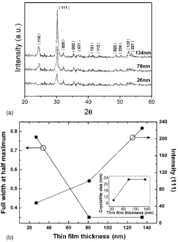
The film thickness strongly influences the structure of the crys-talline phase in the high-temperature annealed film. Figure 2 shows XRD patterns of sol-gel derived ZST thin films with different thick-nesses. The thicker ZST film annealed at 700°C contains a crystal-line phase corresponding to orthorhombic ZST with共111兲, 共110兲, and共002兲 orientations which are well consistent with the ZST
pat-*Electrochemical Society Active Member. z
E-mail: [email protected]
Electrochemical and Solid-State Letters, 9共5兲 F31-F33 共2006兲
1099-0062/2006/9共5兲/F31/3/$20.00 © The Electrochemical Society F31
tern found in JCPDF file no. 81-2214. The 26 nm ZST film has a pronounced preferred orientation. However, it is crystalline if the thickness is 100 nm. The crystallization process includes two mechanisms, nucleation and grain growth. With the shrinking of the film thickness, the surface energy, which favors the suppression of the grain growth, plays a dominant role.21Therefore, under the same annealing condition, the 26 nm film is more difficult to crystallize than the 78 nm film. In addition, the crystal structure of the film is strongly dependent on its thickness. The 26 nm ZST shows an orthorhombic phase with共111兲 orientation, while the 134 nm film shows an orthorhombic phase with multiorientation. The strongest peak is共111兲, which can be explained on the basis of Wulff’s theo-rem since the relative values of ZST thin-film surface energy 共de-fined as the surface energy of the 兵hkl其/ surface energy of 兵111其 ⫻ 100兲, calculated by Nakagawara et al. for 兵111其 and 兵110其 planes are 100 and 120, respectively.10The noise level is high and the only visible peak is seen as in共111兲 for film thickness less than 78 nm. In the XRD spectra, the signal for共111兲 is only four times the noise of the background for film thickness below 78 nm, and the minor peaks, if they exist, are indistinguishable from the background. To clear up this ambiguity, more than four separate experiments were done for each thin film sample. The signals of XRD peaks of the experiments are attached together, and were plotted in one chart. Still only the共111兲 peak is noticeable for film thicknesses below 78 nm. A XRD experiment with longer scan time was also pursued and same result appeared. Therefore, the suggestion is drawn that 26 nm film with preferable direction was obtained. The XRD results show that no other secondary phase is present in the film in Fig. 2, probably due to the sensitivity limit of the instrument or the small volume ratio of the crystal. Further studies using TEM or SIMS are needed to clear up this issue.
The film thickness can further influence the crystal size in the ZST film. With the film thickness increasing, the films shows more intense diffraction peaks共Fig. 2b兲, indicating a greater volume per-centage of the crystalline phases. The insert in Fig. 2 shows the correlation between the crystal size共Dv兲 and the film thickness. According to the XRD line broadening by using Scherrer formula,21
the averaged crystal size for films annealed at 700°C are 10, 23, and 23 nm for 26, 78, and 134 nm films, respectively, indicating the crystal size of polycrystalline ZST films were not increasing with the increase of film thickness and all crystal sizes were smaller than the film thickness and independent of film thickness.
The typical morphology for 700°C annealed ZST film of thick-ness 26 nm was examined by AFM, as shown in Fig. 3. The rough-ness of root mean square共rms兲 of all deposited films was less than 0.9 nm, indicating that smooth ZST films can be deposited on a p-type Si共100兲 substrate using the proposal sol-gel technique. Figure 4 shows a cross-sectional SEM image of a 134 nm ZST film an-nealed at 700°C.20The image demonstrates a smooth coating sur-face on the ZST thin film, also indicating that the film has good Table I. Film thicknesses as function of numbers of coating
cycles.
Number of layers Thickness共nm兲
1 26 ± 6
3 78 ± 1
5 134 ± 8
Figure 1. XPS analysis of the ZST thin film with 78 nm.
Figure 2. 共a兲 XRD patterns and 共b兲 fwhm and highest intensity of sol-gel
derived ZST thin films with different thicknesses annealed at 700°C for 30 min.
Figure 3. AFM image of ZST film with thickness of 26 nm. F32 Electrochemical and Solid-State Letters, 9共5兲 F31-F33 共2006兲
F32
deposition quality. ZST grains with sizes ranging between 15–30 nm were observed in this cross section, which are very close to the crystal sizes calculated in Fig. 2. Additionally, HRTEM analysis shows that about a 4–5 nm interface layer with amorphous phase appears independent of the thickness.
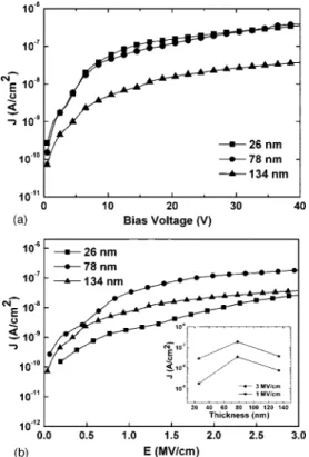
Figure 5 shows the leakage current density of ZST films as a function of bias voltage and applied electric field. The leakage cur-rent densities of polycrystalline ZST film are in the order of 3 ⫻ 10−9and 1.7⫻ 10−7A/cm2at an applied field of 3 MV/cm for
film of thicknesses 34 and 78 nm, respectively. The leakage current of preferred orientation ZST film is in the order of 2 ⫻ 10−9A/cm2at an applied field of 3 MV/cm. Results of this study
demonstrate that the leakage current of preferred orientation ZST is lower than that of polycrystalline ZST, since the high-temperature annealed film forms a polycrystalline phase, which greatly contrib-utes to the high leakage current. Since about a 4–5 nm interface
layer with amorphous phase appears independent of the thickness, the reduced leakage current is more likely to be due to a greater proportion of an amorphous phase present in 26 nm ZST film. Fur-thermore, referring to the inset of Fig. 2b, the crystal size for film of thickness 26 nm is smaller than films of thickness 78 and 134 nm. Because of the presence of more grain boundaries across film with smaller crystal size which would delay the current conduction from one electrode to the other, the lower leakage current density exhibits in 26 nm film.22However, the current density is small enough com-pared to the conventional silicon oxide with the same thickness and well satisfies the target range for the DRAM applications 共1–5 ⫻ 10−7A/cm2兲.2
The prepared ZST films exhibit dielectric con-stants of 15-23. Mays et al. suggested the composition of the CVD-prepared ZST films influences the dielectric constants.19However, the composition of our sol-gel derived films with different thick-nesses shows similar results. The lower dielectric constants as com-pared to those of films deposited by pulsed laser ablation共38兲11may be due to the formation of an interface layer between ZST film and the Si substrate but the value is similar to those of CVD film 共20-30兲21and sputtered films 共11-18兲.15More detailed studies will
be made.
In summary, smooth ZST thin films can be deposited on a p-type Si共100兲 substrate using a sol-gel technique. A ZST film of thickness 26 nm demonstrated a preferred orientation, while films of thickness 75 nm or more illustrate a polycrystalline structure. The crystallite size of ZST films for films of thickness 26, 78, and 134 nm are 10, 23, and 23 nm, respectively. Leakage current densities in polycrys-talline films are higher than those in the preferred orientation film. The order of leakage current density is less than 10−7A/cm at 3 MV/cm from all films, indicating that ZST films with high quality and low leakage current can be obtained by the presented sol-gel process.
Acknowledgments
The authors acknowledge S.S. Wang of Fooyin University for preparing the samples and the Advanced Optoelectronic Technology Center, National Cheng Kung University, Taiwan, for support through equipment and cooperation.
National Nano Device Laboratories assisted in meeting the publication costs of this article.
References
1. S. M. Sze, Physics of Semiconductor Devices, John Wiley & Sons, Inc., New York 共1981兲.
2. The International Technology Roadmap for Semiconductors, 2004, Semiconductor Industry Association, Santa Clara, CA共2004兲.
3. G. D. Wilk, R. M. Wallace, and J. M. Anthony, J. Appl. Phys., 89, 5243共2001兲. 4. Y. Kuo, J. Lu, and J.-Y. Tewg, Jpn. J. Appl. Phys., Part 2, 42, L769共2003兲. 5. J.-Y. Tewg, Y. Kuo, J. Lu, and B. Schueler, J. Electrochem. Soc., 151, F59共2004兲. 6. R. F. Cava, W. F. Peck, and J. J. Krajewski, Nature (London), 377, 215共1995兲. 7. H. Ikawa, A. Iwai, Kazayuki, H. Shimojima, K. Urabe, and S. Udagawa, J. Am.
Ceram. Soc., 71, 120共1988兲.
8. C. L. Huang and M. H. Weng, Jpn. J. Appl. Phys., Part 1, 38, 5949共1999兲. 9. Y. Kim, J. Oh, T. G. Kim, and B. Park, Appl. Phys. Lett., 78, 2363共2001兲. 10. O. Nakagawara, Y. Toyota, M. Kobayashi, Y. Yoshino, Y. Katayama, H. Tabata,
and T. Kawai, J. Appl. Phys., 80, 388共1996兲.
11. C. L. Huang and C. H. Hsu, J. Appl. Phys., 96, 1186共2004兲.
12. R. B. van Dover, L. F. Schneemeyer, and M. Fleming, Nature (London), 392, 162 共1998兲.
13. E. S. Ramakrishnan, K. D. Cornell, G. H. Shapiro, and W. Y. Howng, J.
Electro-chem. Soc., 145, 358共1998兲.
14. D. A. Chang, P. Lin, and T. Y. Tseng, Appl. Phys. Lett., 64, 3252共1994兲. 15. F. J. Wu and T. Y. Tseng, J. Am. Ceram. Soc., 81, 439共1998兲.
16. R. B. van Dover and L. F. Schneemeyer, IEEE Electron Device Lett., 19, 329 共1998兲.
17. W. X. Cheng, A. l. Ding, P. S. Qiu, X. Y. He, and X. S. H. Zheng, Mater. Sci. Eng.,
B, 99, 382共2003兲.
18. Y. Senzaki, G. Alers, A. Hochberg, D. Roberts, J. Norman, R. Fleming, and H. Krautter, Electrochem. Solid-State Lett., 3, 435共2000兲.
19. E. L. Mays, D. Hess, and W. S. Rees, Jr, J. Cryst. Growth, 261, 309共2004兲. 20. Y.-S Ho, M-H Weng, and S.-S Wang, Jpn. J. Appl. Phys., Part 1, 7A, 5125共2005兲. 21. M. Schultz, Diffraction for Materials Scientists, p. 226 Prentice-Hall, Englewood
Cliffs, NJ共1982兲.
22. H. Kang, S. Park, K. Kim, M. Y. Sung, and H. Choi, Electrochem. Solid-State Lett., 7, F70共2004兲.
Figure 4. A cross-sectional SEM image of ZST film with thickness of 78 nm
annealed at 700°C for 30 min. The bottom part is the Si共100兲 matrix and the middle is the ZST coating layer.
Figure 5. The leakage current densities as functions of共a, top兲 bias voltage
and共b, bottom兲 applied electric field of a Al-ZST-p-Si共100兲 MIS structure. The area of the tested capacitor is 1.6⫻ 10−3cm2. Inset in共b兲 shows leakage
current densities of ZST films with different thicknesses applied at 1 and 3 MV/cm.
F33 Electrochemical and Solid-State Letters, 9共5兲 F31-F33 共2006兲 F33