Interfacial Morphology in Polymer Light-Emitting Diodes
Yeau-Ren Jeng,a,zMing-Lung Guo,aHung-Chang Li,aand Tzung-Fang Guob a
Department of Mechanical Engineering, National Chung Cheng University, Ming-Hsiung, Chia-Yi, Taiwan b
Electro-Optical Science and Engineering, Advanced Optoelectronic Technology Center, National Cheng Kung University, Tainan, Taiwan
This work considers the anode at the indium-tin oxide 共ITO兲/poly关2-methoxy-5-共2⬘-ethylhexyloxy兲-1,4-phenylene vinylene兴 共MEH-PPV兲 interface in polymer light-emitting diodes 共PLEDs兲. The surface morphology of ITO is studied by scanning probe microscopy共SPM兲. The mechanical properties of ITO and MEH-PPV are measured by nanoindentation. The results indicate that the surface roughness, defined as the root-mean-square of the surface height on the surface of the ITO substrate, influences the injection of hole-carriers. The injected current is dominated by the tunneling of hole-carriers at the low bias. Increasing the effect contact area at the ITO/MEH-PPV interface lowers the barrier to the injection of holes through the ITO anode to the MEH-PPV light-emitting layer.
© 2007 The Electrochemical Society. 关DOI: 10.1149/1.2789283兴 All rights reserved.
Manuscript submitted June 20, 2007; revised manuscript received August 15, 2007. Available electronically October 8, 2007.
Organic light-emitting diodes共OLEDs兲 have attracted much at-tention because they exhibit high efficiency and high brightness. Their high efficiency results from the effective recombination of oppositely charged carriers, and their high brightness is due to the effective injection of both types of carrier. Recent investigations of the device efficiency have focused on the improvement of either the fabrication process or the materials. However, increasing evidence demonstrates an urgent need to understand the effects of interface morphology.1-3
OLEDs in the bilayer configuration exhibit enhanced injection of charge carriers and high luminous efficiency as reported by Tang et al.4In 2001, Guo et al. presented a template active surface process 共TAS兲.5
They compared the surface topographies formed by TAS and the spin-coating processes. The results revealed the importance of interface topography to device performance. He et al. reported that the root-mean-square 共Rq兲 roughness of the indium-tin oxide 共ITO兲 surface affects device efficiency.6
Yang et al. reported the fabrication of highly efficient polymer LEDs共PLEDs兲 using an in-terfacial layer to modify the cathode interface.7These investigations indicated that device performance is directly related to the formation of a suitable contact interface. In this study, PLEDs were fabricated with various ITO surfaces to examine the influence of the contact interface on the ITO/conjugated polymer interface. The surface con-tact mechanics on the microscale are reported to elucidate the rela-tionship between the surface topography of the ITO anode and the device performance.
The device configuration herein consists of a prepatterned ITO/ glass substrate as the anode, poly关2-methoxy-5-共2
⬘
-ethylhexyl-oxy兲-1,4-phenylene vinylene兴 共MEH- PPV兲 as the light-emissive layer, and an aluminum共Al兲 electrode as the device cathode. The MEH-PPV polymer layer was spin-cast onto the ITO/glass substrate from its toluene solution共concentration was 0.8 mg/cm3兲.Subse-quently, the Al metal electrode was thermally evaporated on the substrates inside a vacuum chamber at 4⫻ 10−6Torr. The current density-voltage共J-V兲 characteristics were obtained using a Keithley 2400 source meter. The luminescent intensity was obtained using a Konica Minolta LS100 luminosity meter.
Potassium hydroxide 共KOH兲/isopropyl alcohol solution 共35 wt %兲 was used to etch the ITO/glass substrate and create vari-ous topographies. Table I summaries the Rqroughness on the ITO/ glass surface and the total effect contact area at ITO/MEH-PPV layer for samples A–C and the barrier height extracted from devices made of samples A–C. In this study, sample A was etched ITO/glass substrate for 20 min by KOH, sample B was etched for 30 min, and sample C was etched for 40 min. The Rqroughness of the etched
ITO/glass substrates was determined using an atomic force micro-scope共AFM, Veeco兲 in tapping mode and is shown in Fig. 1.
Microscopically, the surfaces of the solid films are rough. The area of effect contact between two substrates or films is only a portion of the apparent contact area. Hence, the morphology of the interface results in contact impedance.8Because the charge carriers in the operated PLEDs were injected through the contact interface, the interface morphology determined the efficiency of carrier injection.
Several mechanical properties of ITO and MEH-PPV layers, in-cluding hardness, Young’s modulus, and Poisson’s ratio, must be known to calculate the effect contact area between the ITO/glass anode and light-emitting polymer layer共MEH-PPV in this study兲. The depth-sensing technique of nanoindentation was employed to measure the material’s hardness and Young’s modulus.9The average hardness of ITO was calculated to be 11.16 GPa and the average Young’s modulus was 126.75 GPa. The mean hardness of MEH-PPV was 3.7 GPa and the mean Young’s modulus was 88.55 GPa. The nanoindentation was made by Hysitron. These obtained values were substituted into Eq. 1
1 Er= 共1 − f2兲 Ef + 共1 − i2兲 Ei 关1兴
where Eris the reduced elastic modulus for film and indenter, Efis the Young’s modulus of the thin film,fis the Poisson’s ratio of the
thin film, Eiis the Young’s modulus of the indenter, andiis the Poisson’s ratio of the indenter共⬃0.2兲. The Poisson’s ratios 共f兲 of ITO and MEH-PPV were 0.2 and 0.3,10respectively.
The density of aluminum was 3.96 g/cm3. The thickness of the evaporated aluminum on the device was 200 nm, and the diode area was 0.32 cm2. The mass of the aluminum cathode was calculated to
be 2.5⫻ 10−8kg. Because the weight of the MEH-PPV film was negligible as compared to that of aluminum, the loading on the ITO film can be regarded as 2.5⫻ 10−8kg.
A surface-contact mechanics model11,12was utilized to character-ize the contact area between the ITO and the MEH-PPV film to understand easily the effects of contact areas and surface roughness on the barrier height of the MEH-PPV films. In this model, given the average separation of the surfaces, the total effect area of contact 共At兲 is rewritten as
z
E-mail: [email protected]
Table I. The Rqroughness on the ITO/glass surface and the total
effect contact area at ITO/MEH-PPV layer for samples A–C, and the barrier height extracted from devices made of samples A–C.
Sample A B C
Rq共nm兲 5.58 5.24 5.17
Contact area⫻ 10−3共cm2兲 7.21 6.80 7.17
Barrier height共eV兲 0.12 0.14 0.13
Electrochemical and Solid-State Letters, 10共12兲 D139-D141 共2007兲
At共d兲 = N
冕
d d+
A共z兲dz 关2兴
where N is the total number of asperities, A is the contact area of an asperity deformed elastically,共z兲 is the probability density of the height distribution of the asperities, d is the separation obtained from the asperity heights, z is asperity height measured from the mean of asperity heights, and is interference 共z − d兲. The asperity distribution is assumed to be isotropic and the radius of curvature of an asperity is constructed by a uniform spherical. Because the con-tact behavior between ITO and MEH-PPV film is mainly elastic deformation, the result of the contact is comparable to that given by the model presented by Greenwood and Williamson.13The total ef-fect contact area of samples A–C was calculated from Eq. 2 and summarized in Table I. However, Rq roughness is decreased with
increased etching time of ITO/glass substrates. The surface topogra-phies of ITO/glass samples with different etching times probably result in the difference on the calculation of the total effect contact area.
Figure 2 displays the log J − log V plot of devices made of the ITO/glass substrates with different etching conditions
共sam-ples A–C兲. The log J − log V curves at the low-voltage regime 共⬍2.0 V兲 demonstrate that the current densities of the devices are related to the Rqroughness of the ITO surface. The Rqroughness
and the device current density共⬍2.0 V兲 show a tendency to decline with increased etching time of the ITO/glass substrates. Presumably, the Rq roughness of the ITO surface is an important parameter to influence the injection of charge carriers through the ITO/glass an-ode at the initial and the low-bias regime. The charge carriers tend to be easily accumulated on the tops of the contact peaks and probably are responsible for tunneling through the contact points.
Fowler–Nordheim 共F-N兲 tunneling theory was used to under-stand the tunneling of charge carriers14,15
J⬀ E2exp
冉
−E
冊
关3兴In Eq. 3, J is the current density, E is the electric-field strength, and is a parameter that depends on the barrier shape. Due to the much smaller injection barrier height of holes through the ITO/glass anode than that of electrons from Al cathode, the straight-line ln共J/E2兲 vs
1/E curves共samples A–C兲 as presented in Fig. 3 indicate that the holes are injected into the MEH-PPV layer through the tunneling Figure 1.共Color online兲 AFM-tapping-mode images of etched ITO surface:
共a兲 sample A, 共b兲 sample B, and 共c兲 sample C.
Figure 2. Log J − log V plot for devices made of ITO/glass substrates with different etching conditions:共䊊兲 sample A, 共䉱兲 sample B, and 共+兲 sample C.
Figure 3. F-N tunneling plot of ln共J/E2兲 vs 1/E for devices made of ITO/ glass substrates with different etching conditions:共ⴰ兲 sample A, 共䉱兲 sample C, and共+兲 sample D.
D140 Electrochemical and Solid-State Letters, 10共12兲 D139-D141 共2007兲
process at the beginning of charge injection and are the dominant charge carriers.
The charge carriers共holes兲 are assumed to tunnel through a tri-angular barrier at the polymer interfaces; the constant in Eq. 3 is given by
= 8
冑
2m*3/23qh 关4兴
where is the barrier height and m*is the effective mass of a hole
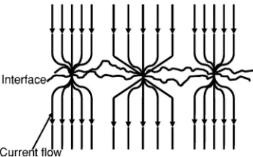
in MEH-PPV, q is the electron charge, and h is Planck’s constant. The injection barriers for the tunneling of holes through the anode in the devices were calculated from Eq. 4. As presented in Table I, it is found that the estimated barrier heights for devices made of different ITO/glass substrates show an inverse trend to the total effect contact area. In the microview conception, the two contacting surfaces con-tact at several concon-tact spots. The sum of the areas of the concon-tact spots equals the effect contact area. The effect contact area deter-mines the contact impedance, as presented in Fig. 4.8A device with a lower effect contact area has a larger contact impedance and a smaller current flow.
This investigation studies the correlation between the interfacial topography, Rqroughness, and the effect contact area in
ITO/MEH-PPV interface. It is found that the KOH/isopropyl alcohol etching process changes Rqroughness of the ITO surface and the total effect contact area between ITO/MEH-PPV. The injection barrier height for holes is related to the total effect contact area. The effect contact area at the ITO/MEH- PPV interface exhibits a correlation on the injection of charge carriers.
Acknowledgments
The authors gratefully acknowledge the support provided to this research by the National Science Council, Taiwan, NSC 95-2120-M-194-001. The support of the Air Force Office of Scientific Re-search under contract no. FA4869-06-1-0056 AOARD 064053 is also acknowledged.
National Chung Cheng University assisted in meeting the publication costs of this article.
References
1. I. M. Chan, T. Y. Hsu, and F. C. Hong, Appl. Phys. Lett., 81, 1899共2002兲. 2. H. Kim, J. S. Horwite, G. P. Kushto, S. B. Qadri, Z. H. Kafafi, and D. B. Chrisey,
Appl. Phys. Lett., 78, 1050共2001兲.
3. A. Andersson, N. Johansson, P. Broms, N. Yu, D. Lupo, and R. Salaneck,
Adv. Mater. (Weinheim, Ger.), 10, 859共1998兲.
4. L. S. Hung, C. W. Tang, and M. G. Mason, Appl. Phys. Lett., 70, 52共1996兲. 5. T. F. Guo, S. Pyo, S. C. Chang, and Y. Yang, Adv. Funct. Mater., 11, 5共2001兲. 6. Y. Hong, Z. He, S. Lee, and J. Kanicki, Organic Light-Emitting Materials and
Devices IV, Paper presented at 46th Annual Meeting, SPIE—The International
Society for Optical Engineering共2001兲.
7. Q. Xu, J. Ouyang, and Y. Yang, Appl. Phys. Lett., 83, 4695共2003兲.
8. R. Holm, Electric Contacts Theory and Application, 4th ed., Springer-Verlag, Ber-lin共1996兲.
9. K. Zeng, Z. K. Chen, L. Shen, and B. Liu, Thin Solid Films, 477, 111共2005兲. 10. XY. Leterrier, C. Fischer, L. Médico, F. Demarco, J.-A. E. Månson, P. Bouten, J.
DeGoede, and J. A. Nairn, 46th Annual Technical Conference Proceedings, p. 856, Society of Vacuum Centers共2003兲.
11. Y. R. Jeng and P. Y. Wang, ASME J. Tribol., 125, 232共2003兲. 12. Y. Zhao, D. M. Maietta, and L. Chang, ASME J. Tribol., 122, 86共2000兲. 13. J. A. Greenwood and J. B. P. Williamson, Proc. R. Soc. London, Ser. A, 295, 300
共1966兲.
14. R. H. Fowler and L. Nordhiem, Proc. R. Soc. London, Ser. A, 119, 173共1928兲. 15. I. D. Parker, J. Appl. Phys., 75, 1656共1994兲.
Figure 4. Schematic of current that passes through the area of contact surface.
D141