Power-Aware Soft Error Hardening via Selective Voltage Scaling
Kai-Chiang Wu and Diana Marculescu Department of Electrical and Computer Engineering
Carnegie Mellon University {kaichiaw, dianam}@ece.cmu.edu
Abstract—Nanoscale integrated circuits are becoming increasingly sensitive to radiation-induced transient faults (soft errors) due to current technology scaling trends, such as shrinking feature sizes and reducing supply voltages. Soft errors, which have been a significant concern in memories, are now a main factor in reliability degradation of logic circuits.
This paper presents a power-aware methodology using dual supply voltages for soft error hardening. Given a constraint on power overhead, our proposed framework can minimize the soft error rate (SER) of a circuit via selective voltage scaling.
On average, circuit SER can be reduced by 33.45% for various sizes of transient glitches with only 11.74% energy increase.
The overhead in normalized power-delay-area product per 1%
SER reduction is 0.64%, 1.33X less than that of existing state-of-the-art approaches.
I. INTRODUCTION
With the emergence of the deep submicron design era, circuit reliability has become a critical challenge for achieving robust systems. Radiation-induced transient errors, hot carrier injection (HCI), and negative bias temperature instability (NBTI) are currently some of the main factors in reliability degradation. As technology scaling proceeds rapidly, digital designs are becoming more susceptible to radiation-induced particle hits resulting from radioactive decay and cosmic rays [1]. A low-energy particle that before had no effect on a circuit can now flip the output of a gate.
Such a bit-flip is called a single-event transient (SET) or a glitch. A single-event upset (SEU) or a soft error occurs if the SET is large enough to be propagated and latched into a memory element.
Although memory elements have suffered from soft errors because of their regular and vulnerable structures, conventional error detecting and correcting codes successfully mitigate the damage caused by soft errors.
However, in logic circuits, even if SETs can be masked via three mechanisms: (i) logical masking, (ii) electrical masking, and (iii) latching-window masking, soft errors are still expected to become more important with continuous scaling trends. Decreasing gate count and logic depth in super-pipeline stages reduce the impact of SET masking since a SET becomes easier to propagate to a latch. Lower supply voltages and node capacitances needed by low power designs not only decrease the critical charge for SETs, but also diminish the pulse attenuation due to electrical masking.
Higher clock frequencies increase the number of latching windows per unit of time and thus facilitate SET latching.
As a result, soft errors in logic become as great of a concern as in memories. A recent study [2] has shown that soft errors would significantly degrade the robustness of
logic circuits, while the nominal SER of SRAMs tends to be nearly constant from 130nm to 65nm technologies. In addition, the SER of combinational circuits is predicted to be comparable to that of unprotected memory elements by 2011 [3]. The importance of soft error hardening for combinational logic was recently emphasized in [4]. As reported by the authors, because sequential circuits usually have more internal gates (combinational logic) than flip-flops (memory elements), the impact attributed to combinational logic is larger than the one attributed to memory elements, when assuming all gates and flop-flops are subject to particle hits proportionally to their respective silicon areas.
In the power optimization domain, voltage scaling is a well-known technique for reducing energy costs by applying lower supply voltages to those gates off critical paths. For SER reduction, voltage scaling is a possible technique which can mitigate SET generation. More specifically, the same amount of charge disturbance produces a smaller (less harmful) SET at gates with high supply voltage (VDDH) than at gates with low supply voltage (VDDL). Level converters (LCs), which impose delay and energy penalties, are needed on the connections from VDDL-gates to VDDH-gates for preventing short-circuit leakage current in VDDH-gates. To minimize the number of LCs, existing methods, whether focusing on power or SER optimization, do not allow any VDDL-VDDH connection in a circuit. In such a case, the optimized circuit is partitioned into two voltage islands: the one (closer to primary inputs) operating at VDDH and the other (closer to primary outputs) operating at VDDL. Nevertheless, as we will see later, restricting the use of VDDH
only near primary inputs cannot prove advantageous for SER improvement in an energy-efficient manner.
The rest of this paper is organized as follows: Section II gives an overview of related work and outlines the contribution of our paper. In Section III, the effects of voltage scaling on circuit SER are explained. In Section IV, we introduce several SER-associated metrics used in this paper. Section V formulates the SER reduction problem. In Section VI, the power-aware soft error hardening framework is presented. Section VII reports the experimental results for a set of standard benchmarks. Finally, we conclude our work in Section VIII.
II. RELATED WORK AND PAPER CONTRIBUTION
Triple modular redundancy (TMR), consisting of three identical copies of an original circuit feeding a majority voter, is the most well-known technique for realizing soft error tolerance. However, for transient errors, TMR induces
excessive (more than 200%) overhead in terms of area and power. Partial duplication [5] targets only nodes with high soft error susceptibility and ignores nodes with low soft error susceptibility. It still involves at least 50% area penalty over the specified requirement and additional delay overhead due to the use of a checker circuit. Gate resizing strategies [6] achieve SER improvement by modifying the W/L ratios of transistors in gates. Potentially large overheads in area, delay, and power are introduced for a significant reduction in SER. Another scheme [7] focuses on flip-flop selection from a given library. This scheme increases the probability of latching-window masking by lengthening latching-window intervals, but does not take into consideration logical masking and electrical masking, which are also dominant factors of circuit SER. A hybrid approach [8] combines gate resizing with flip-flop selection to obtain SER improvement.
A related method [9] uses optimal assignments of gate sizes, supply voltages, threshold voltages, and output loads to get better results with smaller area overhead.
Nevertheless, their results show that, even though LC insertion is avoided, for all benchmarks, all subcircuits finally operate at the highest VDD (1.2V), which dissipates unnecessary power. The algorithm described by Choudhury et al. [10] is another work that employs voltage assignment (dual-VDD) for single-event upset robustness. No LC is needed under the constraint that only high-VDD gates are allowed to drive low-VDD gates, but not vice versa. This implies that soft-error-critical gates, which are of great importance to the soft error rate of a circuit and always close to primary outputs, may not operate at the high VDD unless all gates in the fanin cones are scaled up. Therefore, the resulting voltage assignment is likely to induce unreasonable power penalty.
In this paper, we propose a power-aware SER reduction framework using dual supply voltages. A higher supply voltage (VDDH) is assigned to the gates that have large error impact and contribute most to the overall SER. Since the soft error rate may vary after each voltage assignment, we estimate the effects of VDDH assignments on circuit SER, and accept only those which significantly reduce SER. The end result of this approach is a net reduction in SER under prescribed power constraints. The proposed framework has several advantages over other existing techniques:
z First, the magnitude of gains (i.e., decreases in SER) due to VDDH assignments grows monotonically from primary inputs to primary outputs. A gate which is closer to a primary output always has a larger gain. Such a gate is energy-expensive to be scaled up in the restricted approach [10], but it can be easily identified and assigned VDDH by our approach.
z Second, we develop a very efficient algorithm to minimize SER while keeping the power overhead below a specified limit. To this end, LCs are placed such that the number of up-scaled gates is bounded. It has been verified by our experiments that the appropriate use of LCs is beneficial for the objective of power-aware SER reduction.
z Finally, our framework relies on a symbolic reliability analyzer MARS-C [11], which provides a unified treatment of three masking mechanisms through decision diagrams. Hence, all masking mechanisms are jointly considered as criteria for SER reduction.
III. EFFECTS OF VOLTAGE SCALING
In this section, we explain the effects of voltage scaling in terms of glitch generation and glitch propagation. By changing the supply voltage (VDD) of a gate, the critical charge for transient glitches and the propagation delay of the gate also change. The former, inversely corresponding to glitch generation, is proportional to VDD; the latter, inversely corresponding to glitch propagation, is proportional to VDD/(VDD-VTH)α where α is the velocity saturation factor.
When a gate is scaled up, the same amount of collected charge at its output load will generate a smaller glitch (i.e., lower glitch generation) owing to increased critical charge.
On the other hand, the glitches generated at its fanin neighbors may be propagated with less attenuation (i.e., higher glitch propagation) owing to decreased propagation delay. A chain of FO4 inverters simulated by SPICE in 70nm technology indicates that the effect on glitch generation prevails over the one on glitch propagation.
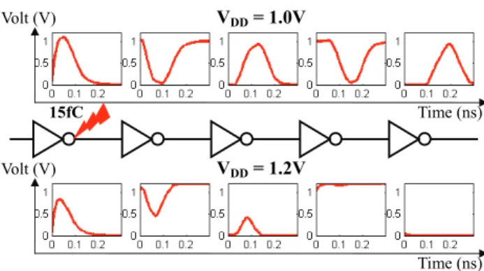
In Fig. 1, we plot the generated and propagated glitches of a transient glitch occurring at the first inverter with 15fC injected charge. The plots on the top (bottom) are made when all inverters operate at VDDL (VDDH). As shown in the figure, after scaling up all inverters, glitch generation of the first inverter decreases and glitch propagation of the remaining inverters also decreases, even though these gates become faster. The principal reason for lower glitch propagation in this case is the decreasing glitch amplitude, which can enhance the effect of electrical masking (attenuation). In other words, electrical masking will be weakened only if the collected charge is large enough to produce a glitch with amplitude at least equal to the supply voltage (full swing). However, electrical masking will be ineffective once the glitch duration exceeds 2X the gate delay. As a result, voltage scaling is certainly feasible for soft error hardening.
IV. SER-ASSOCIATED METRICS
Accurate and efficient SER analysis is a crucial step for SER reduction. Intensive research has been done recently in
Fig. 1. SPICE simulation for glitch generation and propagation VDD = 1.2V
Time (ns) Volt (V)
Time (ns)
Volt (V) VDD = 1.0V
15fC
the area of SER modeling and analysis. Among various modeling frameworks, we choose the symbolic one presented in [11] as the SER analysis engine. This symbolic SER analyzer enables us to quantify the error impact and the masking impact of each gate in a combinational circuit.
As defined in the sequel, these two metrics are useful in deciding whether a gate is critical for being scaled up to the high VDD during selective voltage scaling.
A. Mean Error Impact
For each internal gate Gi, initial duration d and initial amplitude a, mean error impact (MEI) [11] over all primary outputs Fj that are affected by a glitch occurring at the output of gate Gi is defined as:
f F n
k n
j j i
a d
i n n
a d glitch init fails G fails F G
f F
⋅
=
∩ Ρ
=
ΜΕΙ
∑∑
=1 =1 ,
) ) , ( _
( )
( (1)
where nF is the cardinality of set of primary outputs, {Fj}, and nf is the cardinality of set of probability distributions.
The MEI of a gate quantifies the probability that at least one primary output is affected by a glitch originating at this gate. The larger MEI a gate has, the higher the probability that a glitch occurring at this gate will be latched.
B. Mean Masking Impact
D(Gi): the attenuated duration of a glitch at gate Gi; C(Gi): the set of gates in the fanin cone of gate Gi; F(Gi): the set of gates in the immediate fanin of gate Gi; p(Gj, Gi): the set of gates on the paths between Gj and Gi.
For each internal gate Gi, initial duration d and initial amplitude a, mean masking impact on duration (MMID) [12]
is defined as:
d n n
G G G
f G n k
n j
i a d j a
d i
f G
⋅
⋅
→ ΜΙ
=
ΜΜΙ
∑∑
=1 =1
, D ,
D
) (
)
( (2)
where nG is the cardinality of C(Gi), nf is the cardinality of the set of probability distributions, {fk}, and MID(Gjd,a → Gi), masking impact on duration of gate Gi with respect to gate Gj, denotes the absolute duration attenuation contributed by gate Gi on a glitch with duration d and amplitude a originating at gate Gj. More formally, MID(Gjd,a → Gi) can
be defined as: (3)
( )
( )
∑ ∑
∑
∩
∈
−
⋅
=
∩
= Ρ
−
−
⋅
=
∩
= Ρ
=
→ ΜΙ
) , ( p ) ( F
, D
) ( ) ) , ( _ )
( D (
) ( ) ) , ( _ )
( D (
) (
i j i
l G G G
G k l k j k
k
k j
k i
i a d j
D d a d glitch init fails G D G
D d a d glitch init fails G D G
G G
where {Dk} is the set of possible values for glitch duration.
The second summation represents the total weighted attenuation attributed to gate Gi’s immediate fanin gates on the paths between gates Gj and Gi, instead of just gate Gi
itself. Intuitively, MID(Gjd,a → Gi) quantifies how much attenuation can be contributed to gate Gi only, given the duration of glitches originating at gate Gj.
The MMI of a gate denotes the normalized expected attenuation on the duration (or amplitude) of all glitches passing through the gate. The larger MMI a gate has, the more capable of masking glitches this gate is.
V. PROBLEM FORMULATION
We use mean error susceptibility (MES) for evaluating the soft error rate of a circuit. For each primary output Fj, initial duration d and initial amplitude a, the authors of [11]
define mean error susceptibility (MES) as the probability of output Fj failing due to errors at internal gates:
f G n
k n
i j i
a d
j n n
a d glitch init fails G fails F F
f G
⋅
=
∩ Ρ
=
∑∑
=1 =1 ,
) ) , ( _
( )
MES( (4)
where nG is the cardinality of set of internal gates, {Gi}, and nf is the cardinality of set of probability distributions.
In [11], the authors calculate MES for all primary outputs in combinational circuits and with a discrete set of pairs (d, a) of initial glitch durations and amplitudes. Therefore, the probability of primary output Fj failing due to glitches with various durations and amplitudes at different gates is:
−
∑∑
⋅
− Δ
⋅
= Δ Ρ
n m
a d j
j F m n
a a d d
a
F d MES( )
) (
) ) (
( ,
min max min max
(5)
where dm = dmin + m.Δd and an = amin + n.Δa.
Finally, the soft error rate of output Fj can be derived as:
CIRCUIT EFF
PH R A
R ) ( ) (
SER Fj =Ρ Fj ⋅ ⋅ ⋅ (6)
where RPH is the particle hit rate per unit of area, REFF is the fraction of particle hits that result in charge disturbance, and ACIRCUIT is the total silicon area of the circuit.
By using (6), our SER reduction problem is formulated as:
) Gates
# ( ) Gates@V
# ( Subject to
) ( SER Minimize
H DD POs
⋅
≤
∑
∈f F
Fj
j (7)
where f is allowable percentage of gates operating at VDDH. Note that in the minimization problem in (7), SER is a joint function of three masking mechanisms, among which logical masking is pattern-dependent and non-deterministic.
It may not be possible to solve this problem analytically and thereby a heuristic algorithm is required. The number of gates operating at VDDH is constrained by a fraction f of total gate count for bounded energy increase. In the next section, we propose a very efficient algorithm to minimize SER while keeping the numbers of VDDH-gates and required LCs sufficiently low. The basic principle of our approach is to quantify the scaling criticality (SC) of each gate and, under a given power constraint, scale up as many gates with maximum cumulative scaling criticality as possible.
VI. DUAL-VDDSERREDUCTION FRAMEWORK
Before introducing our SER reduction framework, we
first define scaling criticality (SC) for each internal gate. To simplify the following discussion, we omit the initial duration d and amplitude a from the notations of MEI and MMI, but keep in mind that they actually exist. In the circuit in Fig. 2 where all gates operate at VDDL, the MEI value of gate G1 can be expressed as:
[
1 MMI ( )]
) ( MEI )
(
MEIL G1 =Δ+ L G2 ⋅ − LD G2 (8) where MEIL(G2) and MMIDL(G2) are the MEI and MMI values of gate G2 when gate G2 operates at VDDL, and Δ is the amount of gate G1’s error impact propagated to primary outputs through its fanout gates except gate G2 – gates G3
and G4, in this example. If gate G2 is scaled up to VDDH, the MEI value of gate G1, still operating at VDDL, becomes:
[
1 MMI ( )]
) ( MEI )
(
MEIL′ G1 =Δ+ H G2 ⋅ − HD G2 (9) where MEIH(G2) and MMIDH(G2) are the MEI and MMI values of gate G2 when gate G2 operates at VDDH. By subtracting (9) from (8), we have:
[
1 MMI ( )]
MEI ( )[
1 MMI ( )]
) ( MEI
) ( MEI ) ( MEI
2 H D 2
H 2
L D 2
L
1 L 1 L
G G
G G
G G
−
⋅
−
−
⋅
=
− ′ (10)
The difference between (8) and (9), as shown in (10), is the scaling criticality of gate G2. The larger the difference is, the more critical gate G2 is for being scaled up to VDDH. Definition 1: The scaling criticality of gate G is defined as:
[
1 MMI ( )]
MEI ( )[
1 MMI ( )]
) ( MEI ) (
SCG = L G ⋅ − LD G − H G ⋅ − HD G (11) MEIL and MMIDL are obtained during the process of SER analysis for the standard voltage level, VDDL (= 1.0V in our case). Every time the ADD computation and propagation for a gate operating at VDDL are completed, we change the voltage level from VDDL to VDDH (= 1.2V in our case) and then calculate MEIH and MMIDH. It is not necessary to rebuild the ADDs for VDDH since they are isomorphic to those for VDDL. What we need to do is only re-compute the attenuated duration and amplitude in terminal nodes of ADDs by applying the new voltage (VDDH) to the attenuation model.
The scaling criticality of gate G represents the decrease in MEI of gate G’s immediate fanin neighbors after gate G has been scaled up. Based on the definition of MEI, we know that the SER of a circuit greatly depends on the MEI values of its internal gates. This implies that gates with high SC are most critical to be scaled up for soft error robustness.
Definition 2: A gate is called soft-error-critical if its SC is within the highest l% of overall SC values where l is a specified lower bound.
Definition 3: A gate is called soft-error-relevant if its SC is within the next l%-u% of overall SC values where u is a specified upper bound and u is greater than l.
Our objective is to develop a framework which can scale up all soft-error-critical gates and as many soft-error-relevant gates as possible, while incurring the smallest number of LCs and lowest power overhead. The lower bound l for soft-error-critical gates guarantees a significant reduction in SER; the upper bound u for soft-error-relevant gates sets up a power constraint. The algorithm is described in the sequel.
First, we sort all gates (total number of gates being denoted by n) according to their SC values in decreasing order. For each soft-error-relevant gate in the sorted list, we calculate the number of required LCs assuming that gates between the first gate (a soft-error-critical gate) and the current gate (a soft-error-relevant gate) are scaled up. Next, we choose the ith gate (a soft-error-relevant gate; l*n+1 ≦ i
≦ u*n), which has the least required LCs when the 1st gate to the ith gate are scaled up. Finally, we assign VDDH to the first i gates and VDDL to the remaining gates.
Up to this point, all soft-error-critical gates and some soft-error-relevant gates are scaled up so that a significant amount of SER reduction is expected. Nevertheless, there may still be an undesirable number of LCs in the current circuit. Besides extra design costs, (i) soft error susceptibility and (ii) physical design issues will also arise if we do not carefully control the number and distribution of LCs. The following two refinement techniques are used to remove unnecessary LCs.
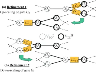
Refinement 1: Scale up some VDDL-gates which are not soft-error-critical to minimize the number of LCs.
Scaling up a VDDL-gate which is not soft-error-critical leads to little improvement in SER, but could reduce the number of LCs needed in the circuit. For example in Fig.
3(a), if we scale up gate G2, LC1-2 needs to be inserted but LC2-3 and LC2-4 can be removed. The number of LCs decreases by one in this case. We try to remove as many LCs as possible using Refinement 1, because the power penalty resulting from a LC is larger than that from the up-scaling of a single gate. This was confirmed by a SPICE
Fig. 3. Effects of two refinement techniques (b) Refinement 2:
Down-scaling of gate G3
(a) Refinement 1:
Up-scaling of gate G2
Fig. 2. Scaling criticality of a gate
simulation (70nm technology) during which we found that the power consumption of a LC [13] is 3.55X the additional power from the up-scaling of a 3-input FO4 NAND gate.
Refinement 2: Scale down some VDDH-gates which are no longer soft-error-critical due to the up-scaling of other gates to further minimize the number of LCs.
A soft-error-critical gate may become non-soft-error- critical if one or more of its fanout neighbors are scaled up.
For example, let gates G3 and G4 in Fig. 3(b) be soft-error-critical and assume that both have been scaled up.
However, as a result of the fact that gate G4 has been scaled up, gate G3 may become non-soft-error-critical since its MEI and SC decrease and may not need to be scaled up. Thus, we can scale gate G3 down back to VDDL and save one LC.
Refinement 1 may increase the percentage of VDDH-gates to exceed the upper bound u, which is specified for limiting the power overhead. Hence, the allowable percentage f of VDDH-gates in our problem formulation (7) should be slightly larger than the upper bound u. In the subsequent section, we will illustrate how the pair (l, u) is decided and how f varies with (l, u). Our overall algorithm for SER reduction, which includes one efficient heuristic and two iterative refinements, is given in Fig. 4.
VII. EXPERIMENTAL RESULTS
We have implemented the dual-VDD SER reduction framework in C++ and conducted experiments on a set of standard benchmarks from ISCAS’85 and MCNC’91 suites.
The technology used is 70nm, Berkeley Predictive Technology Model (BPTM). The clock period (Tclk) used for probability computation is 250ps, and setup (tsetup) and hold (thold) times for output latches are both assumed to be 10ps.
The low supply voltage (VDDL) and high supply voltage (VDDH) are set to be 1.0V and 1.2V, respectively. To calculate SER by (5) and (6), the allowed intervals of initial duration and amplitude are assumed to be (dmin, dmax) = (60, 120)ps and (amin, amax) = (0.8, 1.0)V, with the incremental steps Δd = 20ps and Δa = 0.1V, respectively.
Table 1 reports the experimental results of our proposed framework when the lower bound l is 8 and the upper bound u is 16. That is, we will certainly scale up the first 8% of internal gates (soft-error-critical gates) and minimize the overall SER and the number of required LCs by manipulating the next 8% (soft-error-relevant gates). The inserted LCs are also considered as potential sources of radiation-induced transient glitches. We list the numbers of VDDH-gates and required LCs in columns four and five. The average MES values over all primary outputs before and after selective voltage scaling are shown in columns six and seven. Columns eight and nine demonstrate the MES improvements and possible maximum improvements which are obtained by assigning VDDH to all gates in the circuit.
For instance, circuit C432 has 32 primary inputs, 7 primary outputs, and 156 internal gates. For soft error hardening against glitches with duration 60ps, the numbers of VDDH-gates and required LCs are 31 and 12, respectively.
The average MES of the original circuit is 0.00357, while that of the radiation-hardened version is 0.00205. The MES improvement is 42.50%; the possible maximum improvement by scaling up all (156) gates in circuit C432 is 62.02%. When considering all possible glitch sizes, the overall SER reduction for circuit C432 is 35.28%. On average across all benchmarks, 33.45% SER reduction can
Circuit
# (PIs, POs, Gates)
Dur.
Size (ps)
# VDDH- Gates
# Req.
LCs Ori.
Avg.
MES Opt.
Avg.
MES MES Imprv.
(%) Max.
Imprv.
(%) SER Redctn.
(%) 60 31 12 0.00357 0.00205 42.50 62.02 80 27 13 0.00676 0.00515 23.86 42.85 100 32 11 0.01343 0.00956 28.76 49.89 C432 (36,7,
156) 120 46 9 0.02955 0.01596 45.99 62.64 35.28
60 90 25 0.00194 0.00126 35.14 56.23 80 64 17 0.00413 0.00304 26.40 43.05 100 80 20 0.01229 0.00781 36.46 58.19 C1908 (41,32,
458) 120 74 19 0.02117 0.01544 27.05 54.62 31.26
60 45 23 0.00268 0.00158 41.02 75.29 80 49 15 0.00780 0.00579 25.82 62.25 100 42 19 0.01707 0.01026 39.90 55.05 alu2 (10,6,
339) 120 41 15 0.02736 0.01951 28.68 47.55 33.86
60 57 40 0.00093 0.00049 46.73 53.18 80 94 28 0.00297 0.00190 35.96 65.74 100 106 26 0.00870 0.00656 24.61 67.43 alu4 (14,8,
660) 120 103 27 0.01464 0.01063 27.35 55.34 33.66
60 99 9 0.00062 0.00043 30.68 54.30 80 120 9 0.00147 0.00103 29.54 46.01 100 130 8 0.00233 0.00163 29.99 31.64 frg2 (16,1,
566) 120 125 9 0.00349 0.00247 29.25 30.45 29.86
60 56 27 0.00246 0.00144 41.35 67.00 80 72 22 0.00837 0.00485 42.00 75.25 100 55 24 0.03180 0.01818 42.83 82.10 vda (17,39,
368) 120 80 13 0.06552 0.03527 46.17 77.18 43.09
60 9 0 0.01433 0.00937 34.65 55.09 80 11 0 0.02907 0.01819 37.41 50.78 100 15 0 0.04378 0.02909 33.55 33.72 x2 (10,7,
36) 120 9 0 0.06435 0.04618 28.24 30.77 33.46
60 64 5 0.00208 0.00146 29.73 56.88 80 58 6 0.00377 0.00279 26.06 32.47 100 53 6 0.00589 0.00436 26.06 28.26 x4 (94,71,
288) 120 53 4 0.00872 0.00640 26.66 28.07 27.12
Avg. 18.89% 3.86% 33.45%
Table 1
Mean error susceptibility (MES) improvements for various duration sizes and overall soft error rate (SER) reductions Dual-VDD SER reduction (circuit, n, l, u) {
// n: gate count; l: lower bound; u: upper bound.
Compute scaling criticality (SC) for each gate in circuit;
sorted_gate_list Å Sort all gates by their SC values in decreasing order;
// 1 ~ l*n: soft-error-critical gates; l*n+1 ~ u*n: soft-error-relevant gates.
for (i = 1; i <= u*n; i = i+1) {
Scale up the ith gate in sorted_gate_list;
num_of_LCs[i] Å Calculate the number of LCs needed in circuit;
}
// Find the least required LCs.
index Å Extract the index of minimum in num_of_LCs;
for (i = index+1; i <= u*n; i = i+1) // Keep the first index gates up-scaled.
Scale down the ith gate in sorted_gate_list;
// Refinement 1
for each (VDDL-gate G in circuit)
if (scaling up gate G will not increase the number of required LCs) Scale up gate G;
// Refinement 2
for each (VDDH-gate G in circuit) {
if (gate G is soft-error-critical) // Do not touch soft-error-critical gates.
continue;
if (scaling down gate G will not increase the number of required LCs) Scale down gate G;
} }
Fig. 4. The overall algorithm
be achieved with 18.89% (slightly larger than the upper bound u) of total gates scaled up and 3.86% LCs inserted, as a fraction of the gate count.
In some cases, for example circuit x4, the SER reduction is 27.12%, below the average 33.45%. However, one can note that the MES improvements for 80-120ps duration sizes are very close to the possible maximum improvements.
The results reveal that, by scaling up a small portion of internal gates in a circuit, we can reduce the overall SER either by a significant percentage or near the theoretical minimum. On average, more than three-fifths (33.45% out of 52.85%) of maximum SER reduction is accomplished with less than one-fifth (18.89%) of gates being scaled up.
The runtime of our algorithm is always within few minutes, given the MEI and MMI values of each gate. The corresponding delay and power overheads are shown in Fig.
5, where timing and power are measured by using Synopsys® PrimeTime PX. Input probability distributions used for the results in Table 1 are also applied for switching activity analysis in PrimeTime PX. Our framework adds an average of 11.74% power dissipation, due to the 18.89%
VDDH-gates and 3.86% LCs. Overall, the overhead in normalized power-delay-area product per 1% SER reduction is 0.64%, while that of [9] is 0.85%. Using MEI and MMI described in Sections IV.A and IV.B, we can easily characterize each gate and also apply these techniques, for example, gate sizing [11] for further SER reduction without much additional effort.
The goal of this methodology is to assign VDDH to gates with large scaling criticality. Therefore, after those gates are scaled up, the MEI values of internal gates will become smaller. In Fig. 6, the distributions of overall MEI values for circuit x2 are presented. Each point in the figure denotes the number of gates (y-axis) having MEI within the interval (x-axis). As can be seen, the MEI distribution after optimization shifts toward the left, which means the MEI values of internal gates become much smaller due to selective voltage scaling.
We also perform experiments with different lower and upper bounds. As shown in Fig. 7, the SER reductions when using (l, u) smaller than (8, 16) are not as significant as the case when (l, u) is (8, 16). On the other hand, using (l, u) greater than (8, 16) may induce more VDDH-gates and LCs.
More VDDH-gates will result in higher power penalty; more LCs will lead not only to higher overhead in terms of area and power, but also to larger error impact since LCs are also vulnerable to particle hits.
VIII. CONCLUSION
In this paper, we propose a power-aware soft error hardening framework via selective voltage scaling using dual supply voltages for combinational logic. A novel metric, scaling criticality (SC), is used to estimate the effects of VDDH assignments on circuit SER. Based on the estimation through SC, we introduce an efficient heuristic and two refinement techniques for SER reduction while keeping the numbers of VDDH-gates and required LCs sufficiently low.
Various experiments on a subset of standard benchmarks demonstrate that the proposed framework can effectively reduce the circuit susceptibility to radiation-induced transient errors.
RERFERENCES
[1] R. Baumann, “Soft errors in advanced computer systems,” in IEEE Design and Test of Computers, Vol. 22, No. 3, May 2005.
[2] S. Mitra et al., “Robust system design with built-in soft-error resilience,” in IEEE Computer Magazine, Vol. 38, No. 2, Feb. 2005.
[3] P. Shivakumar et al., “Modeling the effect of technology trends on the soft error rate of combinational logic,” in Proc. Int’l Conf. on Dependable Systems and Networks (DSN), pp. 389-399, Jun. 2002.
[4] N. Miskov-Zivanov and D. Marculescu, “Modeling and optimization for soft-error reliability of sequential circuits,” in IEEE Trans. on Computer-Aided Design of Integrated Circuits and Systems, Vol. 27, No. 5, May 2008.
[5] K. Mohanram and N. A. Touba, “Cost-effective approach for reducing soft error failure rate in logic circuits,” in Proc. Int’l Test Conf. (ITC), pp 893-901, Sep. 2003.
[6] Q. Zhou and K. Mohanram, “Gate sizing to radiation harden combinational logic,” in IEEE Trans. on Computer-Aided Design of Integrated Circuits and Systems, Vol. 25, No. 1, Jan. 2006.
[7] V. Joshi et al., “Logic SER reduction through flipflop redesign,” in Proc. Int’l Symp. on Quality Electronic Design (ISQED), pp. 611-616, Mar. 2006.
[8] R. R. Rao et al., “Soft error reduction in combinational logic using gate resizing and flipflop selection,” in Proc. Int’l Conf. on Computer-Aided Design (ICCAD), pp. 502-509, Nov. 2006.
[9] Y. S. Dhillon et al., “Analysis and optimization of nanometer CMOS circuits for soft-error tolerance,” in IEEE Trans. on Very Large Scale Integration (VLSI) Systems, Vol. 14, No. 5, May 2006.
[10] M. R. Choudhury, Q. Zhou, and K. Mohanram, “Design optimization for single-event upset robustness using simultaneous dual-VDD and sizing techniques,” in Proc. Int’l Conf. on Computer-Aided Design (ICCAD), pp. 204-209, Nov. 2006.
[11] N. Miskov-Zivanov and D. Marculescu, “MARS-C: modeling and reduction of soft errors in combinational circuits,” in Proc. Design Automation Conf. (DAC), pp. 767-772. Jul. 2006.
[12] K.-C. Wu and D. Marculescu, “Soft error rate reduction using redundancy addition and removal,” in Proc. Asia South Pacific Design Automation Conf. (ASP-DAC), pp. 559-564, Jan. 2008.
[13] S. H. Kulkarni and D. Sylvester, “High performance level conversion for dual VDD design,” in IEEE Trans. on Very Large Scale Integration (VLSI) Systems, Vol. 12, No. 9, Sep. 2004.
Fig. 7. SER reductions with different lower & upper bounds alu2
Fig. 5. Corresponding delay and power overheads Max SER reduction
54% 53% 60% 60% 41% Max SER reduction 43% 36% 53%
75%
Fig. 6. Mean error impact (MEI) distributions x2