This article was downloaded by: [National Chiao Tung University 國立交通大學] On: 25 April 2014, At: 06:17
Publisher: Taylor & Francis
Informa Ltd Registered in England and Wales Registered Number: 1072954 Registered office: Mortimer House, 37-41 Mortimer Street, London W1T 3JH, UK
Ferroelectrics
Publication details, including instructions for authors and subscription information:
http://www.tandfonline.com/loi/gfer20
Nonpolar Bistable Resistive Switching
Behaviors of Bismuth Titanate Oxide
Thin Film
Meng-Han Lin a , Ming-Chi Wu a , Chun-Chieh Lin b & Tseung-Yuen Tseng ac
a
Department of Electronics Engineering and Institute of
Electronics , National Chiao Tung University , Hsinchu, 300, Taiwan b
Department of Electrical Engineering , National Dong Hwa University , Hualien, 947, Taiwan
c
Department of Materials and Mineral Resources Engineering , National Taipei University of Technology , Taipei, 106, Taiwan Published online: 20 Sep 2010.
To cite this article: Meng-Han Lin , Ming-Chi Wu , Chun-Chieh Lin & Tseung-Yuen Tseng (2009) Nonpolar Bistable Resistive Switching Behaviors of Bismuth Titanate Oxide Thin Film, Ferroelectrics, 380:1, 30-37, DOI: 10.1080/00150190902870101
To link to this article: http://dx.doi.org/10.1080/00150190902870101
PLEASE SCROLL DOWN FOR ARTICLE
Taylor & Francis makes every effort to ensure the accuracy of all the information (the “Content”) contained in the publications on our platform. However, Taylor & Francis, our agents, and our licensors make no representations or warranties whatsoever as to the accuracy, completeness, or suitability for any purpose of the Content. Any opinions and views expressed in this publication are the opinions and views of the authors, and are not the views of or endorsed by Taylor & Francis. The accuracy of the Content should not be relied upon and should be independently verified with primary sources of information. Taylor and Francis shall not be liable for any losses, actions, claims, proceedings, demands, costs, expenses, damages, and other liabilities whatsoever or howsoever caused arising directly or indirectly in connection with, in relation to or arising out of the use of the Content.
This article may be used for research, teaching, and private study purposes. Any substantial or systematic reproduction, redistribution, reselling, loan, sub-licensing, systematic supply, or distribution in any form to anyone is expressly forbidden. Terms &
Conditions of access and use can be found at http://www.tandfonline.com/page/terms-and-conditions
Ferroelectrics, 380:30–37, 2009 Copyright © Taylor & Francis Group, LLC ISSN: 0015-0193 print / 1563-5112 online DOI: 10.1080/00150190902870101
Nonpolar Bistable Resistive Switching Behaviors
of Bismuth Titanate Oxide Thin Film
MENG-HAN LIN,
1MING-CHI WU,
1CHUN-CHIEH LIN,
2AND TSEUNG-YUEN TSENG
1,3,∗1Department of Electronics Engineering and Institute of Electronics,
National Chiao Tung University, Hsinchu 300, Taiwan
2Department of Electrical Engineering, National Dong Hwa University,
Hualien 947, Taiwan
3Department of Materials and Mineral Resources Engineering, National Taipei
University of Technology, Taipei 106, Taiwan
Nonpolar bistable resistive switching behaviors of sol-gel derived bismuth titanate oxide (BTO) thin film are investigated in this study. The BTO thin film memory device without thermal treatment shows higher resistance ratio (∼104) than the other annealed devices. The resistive switching behavior of the Pt/BTO/LNO/Pt device is reproducible and can be traced over 100 times. Both low resistance state (ON-state) and high resistance state (OFF-state) are stable over 104s under 0.3 V voltage stress at room temperature (RT) and 85◦C. The retention behaviors of both memory states in the Pt/BTO/LNO/Pt device are very stable over 2× 10⁶s at RT and 85◦C, showing that the BTO thin film memory device is a good candidate for nonvolatile memory application
Keywords RRAM; bismuth titanate oxide (BTO); sol-gel method
Introduction
In recent year, flash memory technology plays an important role in modern electronic device due to its nonvolatile characteristics which can hold stored data for a long time without any power supply. However, flash memory device will meet its physical limitation of device scaling in the near future [1]. Several novel memory devices such as phase change memory (PCM), magnetic random access memory (MRAM), ferroelectric random access memory (FRAM), and resistive random access memory (RRAM) are extensively investigated in order to replace flash memory device. RRAM has been considered as a promising candidate for next-generation nonvolatile memory (NVM) application because of its advantages such as low power consumption, low operation voltage, high operation speed, high endurance, long retention, small cell size, nondestructive read out, and simple structure [2]. Several novel materials, including perovskite oxides [2–6], and transition metal oxides [7–10], have been extensively investigated for possible RRAM application. Recently, the resistive switching behavior in bismuth titanate oxide (BTO) deposited by
Received August 3, 2008; in final form December 31, 2008.
∗Corresponding author. E-mail: [email protected] 30
Bismuth Titanate Oxide Thin Film 31
electron cyclotron resonance sputtering was reported [11]. In this study, we report the resistive switching properties of sol-gel derived BTO-based memory device.
Experimental Details
After the standard RCA cleaning, a 200-nm-thick SiO2isolation layer was thermally grown
on p-type (100) Si substrates. A 20-nm Ti adhesion layer and an 80-nm Pt bottom electrode (BE) sequentially deposited on SiO2/Si substrate by an electron beam evaporator at room
temperature. The 100-nm-thick LaNiO3(LNO) buffer layers with (100) and (200) preferred
orientations were deposited on Pt BE by a radio frequency (RF) magnetron sputter, and followed by rapid thermal annealing at 600◦C in O2 ambient for 1 min. The LNO buffer
layer is used for providing better crystallinity of the BTO film. To fabricate BTO thin film, stoichiometric amounts of the starting materials consisting of bismuth acetate (ALDRICH, 99.999%) and Ti isopropoxide (ALDRICH, 97%) were dissolved in acetic acid (FLUKA, 99.8%) and acetylacetone (FLUKA, 99.5%) to form the BTO solution. The above-prepared 0.4 M precursor solution was spin-coated on the LNO/Pt/Ti/SiO2/Si substrates to form sol-gel films, and then annealed at 400, 500, 600, and 700◦C in N2ambient for 1 h. The
sol-gel route for BTO film preparation is shown in Fig. 1. Finally, an 80-nm-thick Pt, with a diameter of 250 µm defined by a metal mask, was used as top electrode to complete the Pt/BTO/LNO/Pt device. The electrical measurements of BTO-based memory device were performed by Agilent 4155C semiconductor parameter analyzer, and the voltage bias was applied on Pt top electrode with grounded-Pt bottom electrode as shown in Fig. 2.
Results and Discussion
Figure 3 shows the field emission transmission electron microscopy (TEM) image of the Pt/BTO/LNO/Pt, indicating smooth interface between Pt top electrode and BTO thin film. X-ray diffraction (XRD) analysis is used to identify the effects of thermal treatment on the crystallinity of the BTO thin films. It indicates in Fig. 4 that the as-deposited and
Figure 1. The sol-gel route for BTO thin film preparation.
32 Meng-Han Lin et al.
Figure 2. BTO thin film device structure. (See Color Plate V)
Figure 3. TEM image of Pt/BTO/LNO/Pt/Ti structure on SiO2/Si substrate.
Figure 4. XRD patterns of as-deposited BTO film and BTO films annealed at 400, 500, and 600◦C for 1 h.
Bismuth Titanate Oxide Thin Film 33
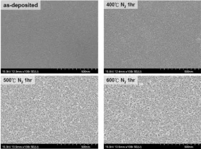
Figure 5. SEM image of as-deposited, 400, 500, 600◦C-annealed BTO films.
400◦C-annealed BTO thin films are amorphous. However, the peaks of BTO thin films appear after 500◦C thermal treatment, showing that the crystalline structure is transformed from amorphous into polycrystalline. To observe the surface morphology of BTO thin films annealed at various temperatures, the top view images of BTO thin films were observed by scanning electron microscopy (SEM) as shown in Fig. 5. The SEM images show that the grain size of BTO thin films increases with increasing annealing temperature, which agrees with the results of XRD analysis.
Before the resistive switching is observed, the original-state current is much lower than high resistance state (OFF-state) current owing to the excellent insulating properties
Figure 6. Typical resistive switching I-V curves of as-deposited BTO thin film. The inset is the
resistance ratio.
34 Meng-Han Lin et al.
Figure 7. Effect of thermal treatment on I-V characteristics of the films. (See Color Plate VI)
of BTO thin film. When applied voltage is swept to forming voltage, the original-state current is suddenly increased and switched to low resistance state (ON-state). The first resistive switching process is called the forming process, which is needed to activate the BTO memory device by performing an electrical stress with proper current compliance. Fig. 6 depicts the typical resistive switching I-V characteristics of as-deposited BTO thin film. When the negative voltage is applied on the top electrode from 0 to−6 V, the memory state of BTO memory device is switched from OFF-state to ON-state at about−3.5 V (turn-on voltage). Then, the bias voltage sweeps from 0 V to−2 V and the memory state is changed from ON-state to OFF-state at about−1 V (turn-off voltage). The resistive switching properties of the BTO memory device altered by either positive or negative bias voltage are called nonpolar resistive switching characteristics. The resistance ratio between ON-state and OFF-state is more than 104.
Figure 8. Statistics of switching voltages for as-deposited, 400, 500, 600, 700◦C-annealed BTO thin films.
Bismuth Titanate Oxide Thin Film 35
Figure 9. Distribution of switching voltages of as-deposited BTO thin films.
Figure 7 shows that the OFF-state current is increased with increasing annealing tem-perature. The increase in OFF-state current might be due to better crystallinity of BTO thin film based on the results of XRD and SEM analyses. However, no obvious influence of thermal treatment on switching voltage is observed in Fig. 8. The switching voltage distributions during continuously 100-cycle operation in the Pt/BTO/LNO/Pt device are shown in Fig. 9. The resistive switching behavior of our device is reproducible and can be traced over 100 times as shown in Fig. 10. It was reported that the resistive switching behavior was caused by the formation and rupture of the conducting filaments [12]. There-fore, the variations present in the ON-state, OFF-state, turn-on voltage, and turn-off voltage of the Pt/BTO/LNO/Pt device, which might be due to the random formation and rupture of the conducting filaments.
As illustrated in Fig. 11, the non-destructive readout characteristics of both ON-state and OFF-state for the BTO memory device is stable over 104s at room temperature (RT)
Figure 10. Endurance test of as-deposited BTO thin film.
36 Meng-Han Lin et al.
Figure 11. Nondestructive readout characteristics of as-deposited BTO thin film at RT and 85◦C. (See Color Plate VII)
and 85◦C, indicating that the two memory states demonstrate good stability under read voltage stress at RT and 85◦C. The retention time, an important characteristics for NVM application, were also measured at RT and 85◦C. Both memory states in the Pt/BTO/LNO/Pt device are stable over 2× 10⁶s and maintain their resistance ratios at least 103 as shown
in Fig. 12.
Conclusions
The physical properties and resistive switching characteristics of sol-gel derived BTO-based memory device are studied in this work. The as-deposited and 400◦C-annealed BTO
Figure 12. Retention behaviors of as-deposited BTO thin film at RT and 85◦C. (See Color Plate VIII)
Bismuth Titanate Oxide Thin Film 37
thin films are amorphous, but the polycrystalline structure is formed for BTO thin films annealed over 500◦C. The as-deposited BTO thin film memory device shows nonpolar switching properties, and the resistance ratio between two memory state is more than 104.
The thermal treatment affects the electrical characteristics of BTO thin films. However, no obvious influence of thermal treatment on switching voltage is observed. The variations in ON-state, OFF-state, turn-on voltage, and turn-off voltage of the Pt/BTO/LNO/Pt device can be attributed to the random formation and rupture of the conducting filaments. The BTO memory device, which shows the stable resistance ratio over 104 s under 0.3 V voltage stress, and long retention behavior (more than 2× 10⁶s), is a good candidate for next-generation NVM application.
Acknowledgments
This work was supported by the National Science Council, Taiwan, under project No. NSC96–2628-E-009–166-MY3.
References
1. A. Chen, S. Haddad, Y.-C. Wu, T.-N. Fang, Z. Lan, S. Avanzino, S. Pangrle, M. Buynoski, M. Rathor, W. Cai, N. Tripsas, C. Bill, M. VanBuskirk, and M. Taguchi, Tech. Dig.-Int. Electron
Devices Meet. 746 (2005).
2. C.-C. Lin, C.-Y. Lin, M.-H. Lin, C.-H. Lin, and T.-Y. Tseng, IEEE Trans. Electron Devices. 54, 3146 (2007).
3. C.-Y. Liu, A. Wang, W.-Y. Jang, and T.-Y. Tseng, J. Phys. D, Appl. Phys. 39, 1156 (2006). 4. J.-W. Park, J.-W. Park, M.-K. Yang, K. Jung, D.-Y. Kim, and J.-K. Lee, J. Vac. Sci. Technol. A,
Vac. Surf. Films. 24, 970 (2006).
5. C.-C. Lin, B.-C. Tu, C.-C. Lin, C.-H. Lin, and T.-Y. Tseng, IEEE Electron Device Lett. 27, 725 (2006).
6. A. Beck, J. G. Bednorz, C. Gerber, C. Rossel, and D. Widmer, Appl. Phys. Lett. 77, 139 (2000). 7. H. Sim, D. Choi, D. Lee, S. Seo, M.-J. Lee, I.-K. Yoo, and H. Hwang, IEEE Electron Device
Lett. 26, 292 (2005).
8. M. Fujimoto, H. Koyama, Y. Hosoi, K. Ishihara, and S. Kobayashi, Jpn. J. Appl. Phys. 45, 310 (2006).
9. M. Fujimoto, H. Koyama, M. Konagai, Y. Hosoi, K. Ishihara, S. Ohnishi, and N. Awaya, Appl.
Phys. Lett. 89, 223509 (2006).
10. S. Seo, M.-J. Lee, D.-H. Seo, E.-J. Jeoung, D.-S. Suh, Y.-S. Joung, I.-K. Yoo, I.-R. Hwang, S.-H. Kim, I.-S. Byun, J.-S. Kim, J.-S. Choi, and B.-H. Park, Appl. Phys. Lett. 85, 5655 (2004). 11. D. Lee, H. Choi, H. Sim, D. Choi, H. Hwang, M.-J. Lee, S.-A. Seo, and I.-K. Yoo, IEEE Electron
Device Lett. 26, 719 (2005).
12. Y. Jin, H. Sakai, and M. Shimada, Jpn. J. Appl. Phys. 45, 3243 (2006).
13. C.-Y. Lin, C.-Y. Wu, C.-Y. Wu, T.-C. Lee, F.-L. Yang, C. Hu, and T.-Y. Tseng, IEEE Electron
Device Letters. 28, 366 (2007).