Quasisuperlattice storage: A concept of multilevel charge storage
T. C. Chang, S. T. Yan, P. T. Liu, C. W. Chen, H. H. Wu, and S. M. Sze
Citation: Applied Physics Letters 85, 248 (2004); doi: 10.1063/1.1772873 View online: http://dx.doi.org/10.1063/1.1772873
View Table of Contents: http://scitation.aip.org/content/aip/journal/apl/85/2?ver=pdfcov Published by the AIP Publishing
Articles you may be interested in
2-bit operation based on modulated Fowler-Nordheim tunneling in charge-trapping flash memory cell Appl. Phys. Lett. 100, 052107 (2012); 10.1063/1.3681145
Formation of silicon germanium nitride layer with distributed charge storage elements Appl. Phys. Lett. 88, 112105 (2006); 10.1063/1.2178868
Trap generation in cycled hot-electron-injection-programed/hot-hole-erased silicon-oxide-nitride-oxide-silicon memories
J. Appl. Phys. 99, 044502 (2006); 10.1063/1.2172724
Inverted sidewall spacer and inner offset oxide process for excellent 2 - bit silicon-oxide-nitride-oxide-silicon memory under 100 nm gate length
J. Vac. Sci. Technol. B 22, 2493 (2004); 10.1116/1.1800354
Three-dimensional self-consistent simulation of the charging time response in silicon nanocrystal flash memories J. Appl. Phys. 92, 6182 (2002); 10.1063/1.1509105
This article is copyrighted as indicated in the article. Reuse of AIP content is subject to the terms at: http://scitation.aip.org/termsconditions. Downloaded to IP: 140.113.38.11 On: Wed, 30 Apr 2014 07:58:29
Quasisuperlattice storage: A concept of multilevel charge storage
T. C. Changa)
Department of Physics and Institute of Electro-Optical Engineering, National Sun Yat-Sen University, Kaohsiung, Taiwan, Republic of China and Center for Nanoscience & Nanotechnology,
National Sun Yat-sen University, 70 Lien-hai Road, Kaohsiung 804, Taiwan, Republic of China
S. T. Yan
Institute of Electronics, National Chiao Tung University, Hsin-Chu, Taiwan, Republic of China
P. T. Liu
Department of Photonics and Display Institute, National Chiao Tung University, Hsin-Chu, Taiwan, Republic of China and National Nano Device Laboratory, 1001-1 Ta-Hsueh Road, Hsin-Chu, Taiwan, Republic of China
C. W. Chen
Institute of Electronics, National Chiao Tung University, Hsin-Chu, Taiwan, Republic of China
H. H. Wu
Department of Physics and Institute of Electro-Optical Engineering, National Sun Yat-Sen University, Kaohsiung, Taiwan, Republic of China
S. M. Sze
National Nano Device Laboratory, 1001-1 Ta-Hsueh Road, Hsin-Chu, Taiwan, Republic of China
(Received 8 December 2003; accepted 19 May 2004)
A concept of the quasisuperlattice storage has been demonstrated in this study. Under suitably operated voltage, two apparent states of charge storage can be distinguished. The memory effects are due to the multilevel storage in the quasisuperlattice. Also, the a-Si quantum wells provide a feasible design for the 2 bit per cell nonvolatile memory devices. The operation of the 2 bit per cell needs to be performed by Fowler–Nordheim tunneling instead of conventional channel hot electron injection. Additionally, the dual read operation of the source and drain sides for conventional SONOS 2 bit/ cell device is not necessary, which simplifies the circuit design engineering. © 2004
American Institute of Physics. [DOI: 10.1063/1.1772873]
Recently, portable electronic devices such as digital cameras, laptops, smart cards, mp3 players, USB Flash, have caught much attention in the market and significantly im-pacted the semiconductor industries. All of the above-mentioned products are based on the device of Flash non-volatile memory. The commercially available Flash memory contains the structure of a poly-Si floating gate(FG), which is served as a charge-trapping layer.1Since the difficulties of consecutive scaling have been faced, a candidate, SONOS nonvolatile memory device, arose and positioned an impor-tant part of the industry.2–5 SONOS possesses a structure similar to FG memory device but silicon nitride is adopted as the charge-trapping layer rather than poly-Si layer.6,7 The SONOS structure has a great potential of scaling the thick-ness of the tunnel oxide down to 1.6 nm and reducing the programming voltage below 5 V.6,8 That, hence, improves the performance of speed of the memory device. However, the SONOS memories hardly reach a data retention for 10 years. This is why the actual use of SONOS memories is limited to military applications needing high radiation hardness.9 In this study, both Si and silicon nitride are uti-lized as the charge-trapping layers and a Si/ silicon nitride quasisuperlattice structure is proposed as the multilevel charge storage. Through the electrical measurements, 2 bit per cell Fowler–Nordheim(FN) tunneling operation has been proposed.
Single-crystal, 6 in. in diameter, 共100兲 oriented p-type silicon wafers were used in the present study. The wafers were chemically cleaned by a standard RCA cleaning, fol-lowed by a dry oxidation in an atmospheric pressure chemi-cal vapor deposition furnace at 925 ° C to form a 3 nm tun-nel oxide. Subsequently, silicon nitride 共Si3N4兲 and
amorphous Si 共a-Si兲 quasisuperlattice of two periods were deposited by low pressure chemical vapor deposition (LPCVD) at 780 and 550 °C, respectively. Each of the four LPCVD layers was controlled to be about 2 nm. A 10-nm-thick tetraethyl orthosilicate (TEOS) oxide was de-posited on the quasisuperlattice as the control oxide layer. To densify the control oxide layer, a steam densification was performed at 982 ° C.10 Via the TEOS oxide deposition and steam densification, the two a-Si layers will be crystallized into micro-crystal or poly-crystal, which depends on the grain size of the Si layers. After the Al electrodes were pat-terned and sintered, capacitance–voltage measurements were performed to investigate the memory effects of the quasisu-perlattice storage共QS2兲 memory device.
Figure 1 shows the ideal energy band diagram of the QS2 memory device at V = 0. The quasisuperlattice of Si3N4 and
a-Si clearly shows the band offsets that can easily trap
elec-trons as the memory elements. The undoped a-Si layers are with a wider band gap than that of the Si substrate. To write the memory device, a positive gate voltage has to be applied to make electrons directly tunnel through the tunnel oxide by FN tunneling. The tunneling electrons may be trapped in the
a)Electronic mail: tcchang@mail.phys.nsysu.edu.tw
APPLIED PHYSICS LETTERS VOLUME 85, NUMBER 2 12 JULY 2004
0003-6951/2004/85(2)/248/3/$22.00 248 © 2004 American Institute of Physics
This article is copyrighted as indicated in the article. Reuse of AIP content is subject to the terms at: http://scitation.aip.org/termsconditions. Downloaded to IP: 140.113.38.11 On: Wed, 30 Apr 2014 07:58:29
trap states of the nitride layers, the interface states between Si3N4and a-Si layers, or the quantum wells of the a-Si
lay-ers. The trapped electrons cause a threshold voltage shift 共⌬Vt兲, memory window, of the memory device, which can be
defined as “1” or “0” according to the different threshold voltages. To erase the memory device, negative gate polarity is applied to make the trapped electrons tunnel back to the channel. The control oxide is utilized to prevent the carriers of gate electrode from injecting into the charge trapping sites by FN tunneling.
Figure 2 exhibits C – V hysteresis after the bi-directional voltage sweeping. The voltage is swept between 4 and 共−7兲 V or 7 and 共−7兲 V. The erasing voltage is fixed at 共−7兲 V. Under the programming voltage of 4 and 7 V, the memory window is 0.1 and 0.93 V, respectively, and increas-ing with the programmincreas-ing voltage. It is worth notincreas-ing that the hysteresis is counterclockwise, which is due to substrate in-jection from the electrons of the deep inversion layer and holes of the deep accumulation layer of Si substrate.11
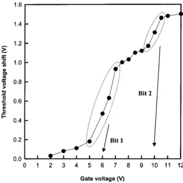
Under varied programming voltages and fixed erasing voltage, the relationship between threshold voltage shift and programming voltage is of special interest. Figure 3 exhibits the gate voltage dependence of the memory window. The threshold voltage shift is increased with the gate voltage. However, there are two sudden rises of the threshold voltage
shift observed, which take place at around 5 and 9.5 V. As the memory device is written with different programming voltages, the tunneling electrons will be captured at the trap states of the Si3N4 layer, the interface states between Si3N4
and a-Si layers, and/or the quantum well of a-Si. During low-voltage programming, the electrons are captured at the charge-trapping sites of trap states of the Si3N4layer and the
interface states between Si3N4 and a-Si layers. The sudden rise implies the charge storage of the a-Si quantum well. Figure 4 shows the band diagram of the memory device un-der programming. The first sudden rise in Fig. 3 is attributed to the charge storage in the a-Si quantum well between two nitride layers. The second sudden rise is deduced that under high-voltage programming the electrons may be written into the a-Si quantum well between nitride and control oxide lay-ers. It is also observed that in Fig. 3 the increments of the two sudden rises are obviously different from each other. The
FIG. 1. The ideal energy band diagram of the QS2memory device at V = 0.
FIG. 2. C – V hysteresis after the bi-directional voltage sweeping. The eras-ing voltage is fixed at共−7兲 V.
FIG. 3. Gate voltage dependence of the memory window. There are two sudden rises of the threshold voltage shift observed, which take place at around 5 and 9.5 V.
FIG. 4. The band diagram of the memory device under programming. Under suitably operated voltage, two apparent states of charge storage can be distinguishable.
Appl. Phys. Lett., Vol. 85, No. 2, 12 July 2004 Changet al. 249
This article is copyrighted as indicated in the article. Reuse of AIP content is subject to the terms at: http://scitation.aip.org/termsconditions. Downloaded to IP: 140.113.38.11 On: Wed, 30 Apr 2014 07:58:29
increment of the second sudden rise is smaller than that of the first one. The threshold voltage shift is due to the elec-trons trapped in the gate dielectrics and the trapped elecelec-trons away from the channel influence the threshold voltage less. Therefore, more considerable threshold voltage shift is ob-served among the first low-voltage charge storage in the a -Si quantum well. In this work the quasisuperlattice storage implies a 2 bit per cell operation by FN tunneling.12 In the design of the multilevel storage, bit-1 can be operated in the
a-Si quantum well between the nitride layers at low voltage
about 5 – 7 V, e.g., 6 V. Bit-2 can be operated in the a-Si
quantum well between nitride and control oxide layers at around 10 V. The 2 bit per cell operation is performed by FN tunneling instead of the conventional channel hot electron injection. Also, the dual read operation of source side and drain side for conventional SONOS 2-bit/ cell device is not necessary, which simplifies the circuit design engineering. To examine the reliability issues of the quasisuperlattice struc-ture, the retention and endurance characteristics have been investigated. As shown in Fig. 5(a), the retention character-istics of the two programming states were strictly performed at the environment of 150 ° C. For each programming state, the memory window remains distinguishable up to 20 h at 150 ° C. Also, the low-voltage programming exhibits a more stubborn retention performance than that of the high-voltage programming. Figure 5(b) shows the endurance characteris-tics of the memory device for low- and high-voltage pro-gramming states. Even 105write/ erase cycles are conducted,
both programming states possess sufficient memory window for a typical sense amplifier to detect and define “1” and “0,” which implies the feasibility of the 2 bit per cell quasisuper-lattice nonvolatile memory devices.
In summary, quasisuperlattice storage has been demon-strated for the concept of multilevel charge storage. In the relationship between threshold voltage shift and gate pro-gramming voltage, two sudden rises were observed. The ob-vious memory effects from the measurements of C – V hys-teresis exhibited two distinguishable charge storages, which can be utilized as a memory device of 2 bit-per cell.
This work was performed at National Nano Device Laboratory and was supported by National Nano Device Laboratory under Contract No. 92A0500001 and the Na-tional Science Council of the Republic of China under Con-tract Nos. NSC92-2112-M-110-020 and NSC92-2215-E-110-006.
1
D. Kahng and S. M. Sze, Bell Syst. Tech. J. 46, 1288(1967). 2
Z. Liu, C. Lee, V. Narayanan, G. Pei, and E. C. Kan, IEEE Trans. Electron Devices 49, 1606(2002).
3
J. J. Welser, S. Tiwari, S. Rishton, K. Y. Lee, and Y. Lee, IEEE Electron Device Lett. 18, 278(1997).
4
J. D. Blauwe, IEEE Trans. Nanotechnology, 1, 72(2002).
5
M. H. White, Y. Yang, A. Purwar, and M. L. French, IEEE International Memory Technology Conference, 1996, p. 52.
6
M. H. White, D. A. Adams, and J. Bu, IEEE Circuits Devices Mag. 16, 22 (2000).
7
D. F. Bentchkowsky, Proc. IEEE 58, 1207(1970).
8
B. Eitan, P. Pavan, I. Bloom, E. Aloni, A. Frommer, and D. Finzi, IEEE Electron Device Lett. 21, 543(2000).
9
H. E. Maes, J. Witters, and G. Groeseneken, Proceedings of the 17th European Solid State Devices Research Conference, Bologna, 1987, p. 157.
10
M. H. White, Y. Yang, A. Purwar, and M. L. French, IEEE International Nonvolatile Memory Technology Conference, 1996, p. 52.
11
D. N. Kouvatsos, V. L. Sougleridis, and A. G. Nassiopoulou, Appl. Phys. Lett. 82, 397(2003).
12
W. J. Tsai, N. K. Zous, C. J. Liu, C. C. Liu, C. H. Chen, T. H. Wang, S. Pan, C. Y. Lu, and S. H. Gu, Tech. Dig. - Int. Electron Devices Meet.
2001, 719(2001). FIG. 5.(a) The retention and (b) endurance of the quasisuperlattice memory
device. Two different programming states were performed and the erasing voltage was fixed at共−7兲 V.
250 Appl. Phys. Lett., Vol. 85, No. 2, 12 July 2004 Changet al.
This article is copyrighted as indicated in the article. Reuse of AIP content is subject to the terms at: http://scitation.aip.org/termsconditions. Downloaded to IP: 140.113.38.11 On: Wed, 30 Apr 2014 07:58:29