行政院國家科學委員會專題研究計畫 期中進度報告
總計畫(1/3)
計畫類別: 整合型計畫
計畫編號: NSC91-2216-E-009-025-
執行期間: 91 年 08 月 01 日至 92 年 07 月 31 日
執行單位: 國立交通大學材料科學與工程學系
計畫主持人: 郭正次
共同主持人: 吳耀銓,陳三元,張立,陳家富,謝宗雍
報告類型: 精簡報告
處理方式: 本計畫涉及專利或其他智慧財產權,2 年後可公開查詢
中 華 民 國 92 年 6 月 2 日
2
行政院國家科學委員會專題研究計畫期中進度
報告
光資訊關鍵性材料製程與性質研究-總計畫(1/3)
計畫編號:NSC91-2216-E009-025
執行期限:91 年 8 月 1 日至 92 年 7 月 31 日
主持人:
郭正次 國立交通大學 材料科學與工程學系
共同主持人:張立、謝宗雍、陳三元、吳耀銓、陳家富
一、摘要
此「系所特色群體計畫」乃以多媒體
時代三個重要光資訊科技:FED、白光 LED、
及光儲存等為整合主題,其未來所需之關
鍵材料及製程是本計畫研究重點。總計畫
下共有 8 個子計畫,個別支援 1~2 個主
題,子計畫之間藉由主題而互相聯繫。各
子計畫大約於第 1~3 年之間分別研發各個
關鍵材料,於第 4~5 年進入組合階段,共
同做成 FED,白光 LED 的原型以及建立高密
度光儲存技術,以驗證材料實際性能並作
回饋改進。以下是各整合主題所含之子計
畫序號及主要工作目標:
FED:(1) 研發低溫下在陰極板上選擇
性成長垂直且均勻的導電性柰米管材料(2)
研發低溫下於陰極板上成長陣列式高導電
性鑽石及類鑽尖端材料(3)研發高亮度、低
電壓電子激發型 RGB 三色螢光粉(8) 研發
FED 真空封裝/結合製程及可靠性分析。
白光 LED:(3)研發高效率、高 CRI 值
光子激發型 RGBY 四色螢光粉 (4)研發 n/p
型 ZnO 磊晶材料做成高效率之 ZnO UV LED
(5)研發以晶圓接合製程達到低缺陷高效
率之 GaN LED。
光儲存:(4)研發 n/p 型 ZnO 磊晶材料
做成高效率之 ZnO UV 光源 (5)研發以晶
圓接合製程達到低缺陷高效率之 GaN 雷射
光源 (6)研發先進光碟材料與結構,及遮
罩層與光開關層材料 (7)研發一維及三維
ZnO 柰米線材做成之 UV 雷射光源 (8)研發
低損耗之光傳輸材料與近場光學讀寫頭製
程。
關鍵詞:光資訊,FED,白光 LED,光儲
存
Abstract
In this program project, we will focus on key materials and processes related to important
optical information technologies in the
multimedia age, FED, white LED and optical storage, as three main themes. There are eight subprojects, each of which involves one or two main themes, and are related to each other through the main themes. Subprojects will investigate independently the critical materials of their interest in the first three years, and work out together prototypes of FED, white LED and optical storage in the 4th and 5th years. The actual properties of the critical materials will be evaluated according to the performance of the prototypes and will be improved through the feedback processes.
The following are the sequence number and aims of the subprojects involving in each main themes:
FED : (1) Selective growth of uniform, vertical, conductive nano-tubes on cathode substrates at low temperature (2) Growth of high conductive diamond or diamond like tip arrays on cathode substrates at low temperature (3) High-brightness and low-voltage RGB phosphors for cathodoluminescence. (8) Vacuum packaging, bonding process, and reliability for FED.
White LED : (3) High-efficiency,
high-CRI-value RGBY phosphors for
photoluminescence (4) n/p type ZnO epitaxial materials for high-efficiency ZnO UV LED (5) Low-defect density, high-efficiency GaN LED fabricated by wafer bonding technology.
Optical storage : (4) n/p type ZnO epitaxial materials for high-efficiency ZnO UV
light source (5) Low-defect density,
high-efficiency GaN laser fabricated by wafer bonding technology. (6) Materials and structures for advanced optical disc, mask layer, and photo-switch layer (7) One- and three-dimension ZnO nano wire materials for UV laser (8) Low loss materials for optical transmission, and
fabrication process of near-field optical
read-write head.
Keywords: optical information technology,
FED, White LED, optical storage
二、前言及研究目的
我國電子產業自民國 60 年代以來,在
產、官、學、研等積極投入經營下,至今
卓然有成。其中尤其以半導體產業(含設
計、晶圓代工、封裝)在過去 10 年間發展
快速,在 2000 年國內產值達 5000 億台幣。
同時帶動相關產業成長,促成國內上一波
的經濟發展。光電科技在其帶動之下突飛
猛進,產品推陳出新,應用層面涵蓋通訊、
資訊、生化、醫療、工業、能源與民生等
領域。光電產業因而被視為我國繼半導體
之後的另一明星產業。其優異表現具體反
映在其產值的快速成長;依光電科技工業
協進會之統計資料,我國在 2000 年之光電
產值為 3,426 億元,預計到 2004 年可達
7300 億,將與半導體產業媲美相等,甚至
超前。吾人可以預期它將帶動國內下一輪
經濟的大幅成長。本計畫的具體工作以
FED、白光 LED、及高密度光儲存等為整合
主題,研發其關鍵性材料,含製程創新與
特性研究。此三個整合主題兼具學術前瞻
性與應用價值。
顯示 FED 構想已經逐漸可行。但要達
到上述理想品質,在材料及製程方面還有
很大空間可以改進,如:
(a). CNT 可在很低的電場下即能發射電子
(~1 V/μ
m)
,且電流密度甚高(mA/cm
2~A/
cm
2)
,耐久性良好,是目前備受注意的尖端
材。其他種導電柰米管也有潛力作為尖端
材。如何利用催化媒使在低溫下(< 500℃)
於陰極板上特定陣列微區內,以垂直方向
成長出均勻長度且具有導電性之柰米管
(NT)
,乃是未來要努力的研發主題。
(b). 以 CVD 方式成長鑽石尖端材比鉬、
鎢、或矽更具耐久性,且有相類似的電流
密度。如何在低溫下於陰極板上選擇性成
長具有高導電性之鑽石及類鑽尖端材是一
個重要的研發主題。
(c). 尖端材與螢光粉之間距約為 1 mm,相
對跨接電壓為~ 5 kV,比 CRT 的電壓(15 kV
~30 kV)降低甚多。由於傳統用螢光粉均
以硫化物為主,在 5000 V 雖然有足夠的亮
度,但會釋放含硫氣體,沈積污染附近的
尖端材料使其劣化。氧化物螢光粉是可能
的替代品,但亮度比硫化物低甚多。若在
低壓運作則需要大為增加電流以達到相同
亮度。此大電流將使螢光粉快速劣化。因
此,RGB 三色高效率的氧化物螢光粉是未來
亟需要突破的研發主題。
(d). FED 的真空封裝有不少課題有待研
發,包含:基板玻璃與微型 spacer 之間接
合(玻璃膠,低溫金屬膠,陽極接合)製
程反應及相容性;基板內各種材料在長久
真空操作環境下將釋放微量氣體,其與尖
端材表面反應而改變 work function 之分
析。
高亮度藍光 GaN LED 已於 1993 年日本
日亞公司研發成功,接著該公司於 1996 年
量產白光 LED(15 lm/W, CRI~75)後,吸
引全球 LED 業者注意,紛紛將白光 LED 列
為研發重點。如何降低價格及提高發光品
質(CRI > 80)及效率(未來達到~50 lm/W)
是未來主要的課題。在材料及製程方面仍
有很大的改進空間,略述如下:
(a). 由於 GaN 磊晶與成長基板 Al
2O
3單晶
間的晶格匹配差為~13%,有相當高的錯位
4
缺陷(dislocations)密度出現於磊晶內
部,導致發藍光效率降低。如何利用晶圓
接合製程以消除 GaN 錯位的研究是一重要
的題目。
(b). 目前對 UV LED 的研究較集中於 ZnO
磊晶(Eg = 3.37 eV)的製程開發,其成
長用的基板可直接採單晶 ZnO,而可得品質
良好的晶格。ZnO 因內部常有氧缺陷而成為
n 型半導體。但是 LED 所必須的另一 p 型
ZnO 截至目前卻是難以成長。如何選擇控制
dopant 以做成 p 型達到高效率的 ZnO UV
LED 是一個重要的題目。
(c). 螢光粉受藍光或 UV 光激發後產生螢
光的能量轉換效率是影響整體效率的重要
一環,此部分受制於 Stokes Shift,材料
組成,純度,製程等因素。目前最有效率
的藍光轉化為黃光之螢光粉為日亞公司開
發 的 釔 鋁 石 榴 石
YAG
系 列
(YGd)
3(AlGd)
5O
12:Ce
3+garnet。研發高效率
黃色(藍光激發)及 RGB 三色(UV 光激發)
螢光粉是另一個重要的題目。
目前全球光碟讀寫頭技術與生產被日
系廠商所主控,我國光碟機廠商的產量均
受制於此關鍵組件,此實為我國光資訊產
業亟待掌握之技術。國內雖有宏景,亞洲
化學等廠商引進技術,作組裝少量產出,
然讀寫頭所需之紅光雷射 LD 仍須進口。國
聯光電最近將已可量產紅光雷射,因此短
波長雷射及其讀寫頭是未來國內下一步努
力之目標。
(a). 藍光或 UV 等短波長雷射是高密度光
碟讀寫頭之要件,它們的開發是光儲存的
重要研究子題之一。如何在材料製程改進
以得到高功率、高可靠度的 GaN 藍光雷射
二極體,ZnO UV 光源,以及柰米結構 ZnO UV
雷射光源是本主題的研究重點。
(b). 近場光學記錄技術也是目前提升光
記錄密度的熱門技術之一。使用近場光學
記錄技術必須儘可能使讀寫頭靠近光碟
片,如此才能使光點縮小的效應耦合進入
碟片而產生近場光學的效果,在如此微小
的工作距離下,光碟機讀寫頭的設計及其
與光碟之間的磨潤學(Tribology)也就變
得極為重要,也是目前近場光學記錄技術
實用化最大的困難。此外,若使用光纖在
進行訊號存取,目前最大的困難則是光纖
的能量消散效應會損耗雷射光之訊號強
度,而使訊號偵測變得極為困難,因此近
場光學讀寫頭組件與低損耗光傳輸材料之
研發為光儲存另一重要研發題目。
(c). 新型結構的碟片、材料以及能突破現
行光繞射極限的資料存取技術亦是重要的
研究子題。包含下列工作:遮罩層(Mask
Layer) 材 料 、 光 開 關 層 (Photo-switch
Layer)材料研究,以突破光繞射極限及光
碟 容 積 。 以 及 提 升 光 碟 之 覆 寫 性 質
(Cycleability) , 研 製 高 密 度 光 碟 母 模
(Mastering)。
三、目前研究進度
子計畫:碳基柰米結構材料之製程及其在
場效顯示器上之應用
有效的選擇性控制碳奈米管成長的位
置對奈米元件的未來應用是一項重要的論
點,本研究將提出一個以自我組裝分子層
N-(2-aminoethyl)-3-aminopropyltrimet
hoxsilane 的技術來控制碳奈米管選區成
長的方法。圖 1 為以自我組裝分子層技術
成長碳奈米管的實驗流程圖。首先為了達
到選區沉積分子層的目標,矽晶片將以低
壓化學氣相沉積法與微影蝕刻技術製備出
非晶質矽/氮化矽的圖案分佈。由於化學選
擇性上的不同,分子層表面活性的前端官
能基反應性與非晶質矽作用會大於與氮化
矽 的 作 用 , 因 此 分 子 層 可 達 到 選 區 的 分
佈。形成選區分佈的分子層末端官能基乙
二胺會先鉗合住鐵離子,之後鐵離子由化
學還原劑還原成奈米粒子。結果,鐵的奈米
粒子選擇性沉積在想要的微圖案上。最後,
選擇性圖案分佈的碳奈米管將可由微波電
漿化學氣相沉積法成長出。
如圖 2 所得接觸角量測儀的資料顯
示,此分子層在非晶質矽晶片表層所形成
的 2-D 界 面 具 有 相 很 強 的 親 水 性 質
(~30o)。由於分子層末端的乙二安化學官
能基具有較強的親水性的效果,因此在分
子層的製備上可很容易作初步的判斷。另
外,分子層的表面與固化沉積後的鐵基奈
米粒子的化學成分鑑定可由化學分析電子
能譜儀(ESCA)得到確認。由圖 3(a)中的資
料顯示氮 1s 的訊號峰值出現在 402ev 左
右,而氮的峰值強度隨著自我組裝分子層
的沉積時間而增強。另外,圖 3(b)中之
Fe3+離子固化後的鐵基奈米粒子呈現的
Fe2p3/2 訊號峰值約落於 713 ev,這顯示
被固化後的鐵離子並無法達到金屬態而是
以氧化態的形式沉積在自我組裝分子層的
表面。
圖 4(a)-4(c) 為擇區成長碳奈米管後
的掃描式電子顯微鏡圖(SEM),在圖 4(a)
中可看出梳形圖案分布的碳奈米管。在圖
4(b)、4(c)中碳奈米管僅成長在非晶質矽
的表面而非氮化矽的表面,這表示以自我
組裝分子層之技術來達到碳奈米管擇區成
長具有很高的效率。而圖中不規則碳奈米
管方向? 符合文獻中不加偏壓所成長的碳
奈米管形貌。的圖 5 所呈現的是碳奈米管
在穿透式電子顯微鏡下(TEM)的碳奈米管
的影像,由 TEM 的照片中可清楚看出圖中
似竹節狀的碳奈米管之末端包覆著一顆鐵
奈米觸媒,因此碳奈米管的成長機制可被
確認是由觸媒頂端開始成長的模式。
Fig.1 以自我組裝分子層技術成長碳奈米
管的實驗流程圖
Fig.2 以接觸角測量儀量測自我組裝分子
層 APTMS 沉積在基材表面後的表面親水性
之結果
Fig.3 化學分析電子能譜儀(ESCA)鑑定分
子層與鐵基粒子的化學成分。 (a)自我組
裝分子層 APTMS 之 N
1s的訊號。(b)鐵基奈
米粒子之 Fe
2p3/2之訊號
6
Fig.4 擇區成長碳奈米管後的 SEM 照片
(a)10um。(b)2um。(c)0.5um
Fig.5 碳奈米管的 TEM 照片
子計畫:磊晶氧化鋅之製程及特性研究
在這個子計畫內容中,成長磊晶之 ZnO
薄膜為主要目標,我們嘗試以 CVD 機台成
長 ZnO 在 GaN/ Sapphire 上,主要考量因
素為 ZnO 和 GaN 之晶格常數相當皆近,其
差異僅約為 2.1%。
圖一為成長 ZnO 薄膜於 GaN 基材上之
AFM 影像,由結果知,CVD 可成長相當平整
之 ZnO 薄膜,其表面粗糙度平均為 8 nm。
XRD rocking curve 之結果則顯示於圖
二,經量測 ZnO(0002)之半高寬量值為 291
arcsec,顯示 CVD 可成長結晶及方向性相
當高之 ZnO 薄膜。
經 10 K 量測之冷激光光譜結果如圖三
所示,於能量 3.37eV 處可得一相當陡峭之
band edge emission 波峰(圖 3a),量測其
半高寬值僅為 18 meV 且其 deep level
emission 顯示相當少,表示 CVD 成長之 ZnO
薄膜其內部缺陷或雜質含量相當少。我們
也嘗試了解溫度變化對 ZnO 薄膜之發光特
性影響,結果顯示於圖 3b,發現隨著溫度
增加其 band edge emission 將往低能量移
動,主要因素為 donor-bound-excitions.
之 thermal dissociation 造成。
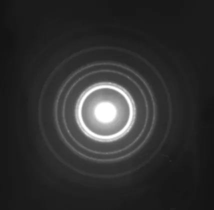
圖四為 TEM 影像觀察之結果,典型之
ZnO 成長於 GaN 上之 TEM 明視野影像如圖
4a 所示,可顯示 ZnO 薄膜內存在對比相當
明顯之 grain size,我們亦嘗試以繞射圖
譜(DF)(4b)探討 ZnO 成長於 GaN 基材上之
結晶順向性,結果顯示,CVD 可直接成長磊
晶之 ZnO 薄膜於 GaN 基材上,且 ZnO 及 GaN
之介面是相當平坦化。
圖一 成長 ZnO 於 GaN 之 AFM 表面影像
16.8 16.9 17.0 17.1 17.2 FWHM 291 arcsec In te n si ty 2 Theta
(0002) ZnO
圖二 XRD rocking curve 結果
圖三 ZnO 於 GaN 基材上之冷 激光光譜
(a)10 K and (b)Temperature Dependence
圖四 TEM 影像觀察結果 (a)TEM Bright
Image、(b)Diffraction Pattern
子計畫:用晶圓接合與溼式蝕刻方式來剝
離側向覆蓋生長之氮化鎵磊晶層
本子計畫主要的目的在於解決氮化鎵
(GaN)薄膜異質磊晶(heteroepitaxial)
於藍寶石(sapphire)基材所衍生的許多
問題。期望藉由晶圓接合(wafer bonding)
搭配濕式蝕刻(wet etching)於側向覆蓋生
長磊晶片(ELOG GaN)上,轉移氮化鎵磊晶
層於它種基板上。
本實驗室在上一期的計畫中,已利用
雷射剝離技術成功的將氮化鎵薄膜轉移到
導熱性質良好且具導電性的銅基板上。然
而,雷射移除法雖然能成功的轉移氮化鎵
磊晶基板,但仍有很多缺點有待改進。其
中最難克服的因素是雷射分離法是一種利
用物理(局部加熱氮化鎵)方式作用於氮
化鎵磊晶層上達到分離氮化鎵磊晶層與基
板目的的方法。這個分離方法本身即是一
種破壞磊晶層的步驟。此外,對於大面積
的磊晶層,其也無法大量生產。為了能成
功轉移氮化鎵磊晶層,並避免使用物理方
式來去除氧化鋁基板,我們利用化學原
理,於不損害氮化鎵磊晶層的前提下分離
氮化鎵磊晶層與生長基板。利用化學選擇
性 蝕 刻 技 術 ( chemical selective
etching)搭配側向覆蓋生長法生長之氮化
鎵磊晶層與晶圓接合技術來轉移氮化鎵磊
晶層的新方法。氮化鎵側向覆蓋成長磊晶
層的圖示如圖一(b),其側向覆蓋成長法
有別於傳統磊晶成長方式【圖一(a)
】
。
在氮化鎵側向覆蓋成長法當中,會鍍
覆數百至一千埃(Å)的非晶系薄膜材料 ,
由於該遮罩層(mask)通常採條 狀方式塗
佈,選擇適當化學蝕刻液,將晶圓接合後
之試片浸泡於蝕刻遮蔽層,但不蝕刻氮化
鎵磊晶層的蝕刻液中。藉由不同的方式促
進選擇性濕式蝕刻的進行至遮罩層完全去
除。在去除遮罩層之後的試片,其磊晶層
與下方緩衝層中即產生條狀的簍空區域,
3.24 3.30 3.36 3.42 (c) In ten si ty (a .u .) Energy (eV) 10k 20k 30k 40k 50k 60k 80k 100k 120k 140k 160k 180k 200k 230k 260k 290k T 2.0 2.2 2.4 2.6 2.8 3.0 (b) P L In te n s ity ( a .u .) Energy (eV) 2.0 2.2 2.4 2.6 2.8 3.0 3.2 3.4 3.6 EX-3LOEX-2LO EX-1LO EX D0X (b) P L I nte n si ty ( a. u.) Energy (eV) 2.0 2.2 2.4 2.6 2.8 3.0 3.2 3.4 3.6 EX D0X (b) P L Int e n si ty (a .u.) Energy (eV)(a)
100nm8
亦即,氮化鎵磊晶層與下方緩衝層的接觸
面積隨之減少。此時即可利用應力集中之
物理特性直接藉拉伸的方式將氮化鎵磊晶
層與基板分離。
試片依其材質,可分為二組。第一種
是尤其他單位提供的 ELO GaN,另一種適用
其他材質來模仿晶圓接合及剝離過程。
(1) ELO GaN 之晶圓接合及分離
其中遮罩層是由 SiO2 所構成。在長
ELO GaN 前,其原始的厚度為 1000 埃。在
與矽晶圓接合後,以這樣的遮罩層厚度,
應可藉著化學蝕刻液將 SiO2 遮罩層去除
掉,並分離 ELO GaN 與 sapphire 基板。如
圖二所示,我們是可在局部地區,得到局
部剝離的 ELO GaN。可惜的是,這只是局部
剝離的 ELO GaN,我們一直都無法有效完整
的剝離整個 ELO GaN 層。檢視其原因,主
要是因為在長完 ELO GaN 後,1000 埃的 SiO2
遮罩層只剩下 300-500 埃(Å)。大部分的
SiO2 層,在長完 ELO GaN 時,都被消耗光
了。由於毛細現象,蝕刻液無法有效的進
去被挖空(腐蝕)的 SiO2 層(通道)
,以
繼續去除 SiO2。而只能形成局部的 under
cut。所以剝離時,只能得到局部剝離的 ELO
GaN。且由於應力的關係,所剝離的 ELO GaN
性質有一點下降。
這部分解決的方法有二。一方面我們
正在與合作的單位商談,希望他們可以提
供較厚的 SiO2 遮罩層之 ELO GaN。一方面,
我們也想辦法聯若廠商,SiO2 遮罩層之厚
度大於 1000 埃之 ELO GaN。
(2) 其他材質來模仿晶圓接合及剝離過程
在未得到夠厚的 SiO2 遮罩層之 ELO
GaN 前,由於 ELO GaN 不易成長且價格昂
貴,我們因此就用其他材質來模仿晶圓接
合 及 剝 離 過 程 。 藉 著 一 系 列 的 SiO2 ,
amorphous Si (α-Si)與 Glass 模擬試片的
製備與實驗流程如圖三所示。
a. 先在 SiO2/α-Si/Glass 試片上利用微影
製程定義出寬度 500µm 的長條形圖案(圖
三 1)
,隨後移除第一層暴露的 SiO2(圖三
2)。
b. 將上步驟的試片浸入複晶蝕刻液用作
除去
α-Si(圖三 3)。
c. 除去最上層光阻(圖三 4)
。再將試片浸
入溶液移除殘餘 Poly-Si(圖三 5)
。此時
試片結構僅剩 Patterned α-Si/Glass 兩
層。
d. 利用高分子膠將上述試片與另一玻璃
基板接合,完成模擬試片。
其中高分子膠的部份為模擬 ELO GaN
的區域,α-Si 則是用作模擬遮罩層材料,
玻璃基板則是模擬氧化鋁基板。
礙於 ELO GaN 之 SiO2 遮罩層的厚度甚
薄(500Å),毛細現象具有很大程度的影
響。因此實驗上的首要目的,除了等待較
厚的 SiO2 遮罩層之 ELO GaN 時,即為移除
遮罩層在遭受蝕刻後殘留在 500Å 通道上
的產物。這將不易在一般條件下完成,因
此必須改變實驗的環境與參數,以下分別
為各種不同環境下的實驗:
(a) 單純利用 KOH:
經過 20 小時後的蝕刻,
α-Si 通道的清
除如圖四所示。雖經過 20 小時的蝕刻,也
僅有靠近表面的
α-Si 被蝕刻。主要的原因
應是 KOH 蝕刻液與蝕刻產物進出通道的不
易。也再次的證明毛細作用是我們蝕刻
α-Si 通道的最大障礙。
(b) 利用超音波震盪器:
將浸泡在 KOH 蝕刻液的試片,放在超
音波的振盪器中。在經過 1.5 小時後,如
圖五,我們確實可看到部分
α-Si 通道的清
除。但當我們拉長振盪時間,並未發現有
更好的效果。也就是說,超音波振盪也有
其限制,要更深入
α-Si 通道需要更長的時
間。這樣的結果,表示整個
α-Si 的蝕刻,
也許已經變成是擴散 control。若是這樣,
KOH 蝕刻液與蝕刻產物,要經過擴散分別到
達
α-Si 或排到通道外,蝕刻的速度當然很
慢。
(c) 利用電場:
為了加強 KOH 蝕刻液與蝕刻產物在
α-Si 通道上的流通,我們也嘗試用電場來
加強其擴散過程。可惜的是,其效果尚未
明朗化。試片不容易用 OM 觀察。效果尚未
定論。
氮化鎵 Mask ( )a 傳統氮化鎵磊晶 ( )b 氮 化鎵側向覆蓋成長
圖一 氮化鎵側向覆蓋成長磊晶層示意
圖二 局部剝離的 ELO GaN
光 阻 SiO2 其他 基 板 高 分 子 膠 Amorphous Glass圖三 模擬氮化鎵側向覆蓋成長遮罩層示
意
圖四 經過 20 小時的 KOH 蝕刻後,α-Si
通道的蝕刻不多,α-Si 通道的寬度為
500μ
m
圖五 經過 1.5 小時的 KOH 的超音波的振
盪,部分 α-Si 通道清除
子計畫:光記錄媒體材料、性質及其應用
於光碟記錄容量提升之研究
本計畫第一年度之研究包含光碟覆寫
性質之提升與光遮罩/光開關層材料之開
發。我們以介電層摻雜 N2O 的方法提升其
機械性質來增加光碟抗雷射之加熱之能
力,目前已建立最佳之摻雜條件,將其植
入光碟之製作後即可驗證其對覆寫性質之
提 升 能 力 。 微 晶 玻 璃 (Semiconductor-
doped Glass,SDG)被應用於光遮罩/光開
關 層 材 料 之 製 備 , 本 計 畫 以 溶 凝 膠
(Sol-gel)與貼靶濺鍍法在 SiO2 中長成奈
米分佈之 CdSe 微粒,藉尺寸縮小造成之藍
位移效應調整其能階值以符合光遮罩/光
開關層之應用。
(一) ZnS 摻雜 N2O 之實驗結果:不同
N2O 摻雜濃度的 ZnS 薄膜表面粗糙度、n&k
值(波長 633 nm)、及其對應之硬度值分別
如圖 1 至 3 所示。由圖 1 可知 15%之摻雜以
下,表面粗糙度隨摻雜濃度之變化不大,
大於 20%的摻雜濃度其表面粗操度增加且
有不規則變化;圖 2 顯示除摻雜濃度為 10%
之外,其餘摻雜濃度之 n&k 值大致相同並
無變化,其光學特性大致與未摻雜 N2O 之
10
ZnS 介電層無明顯差異。圖 3 顯示摻雜濃度
為 15%時,其 ZnS 薄膜具有最高的硬度值,
圖 1 亦顯示此一條件之薄膜表面粗糙度亦
低,故其具有較未摻雜 N2O 之 ZnS 介電層
更強的機械性質,而能提高光碟在覆寫時
產生反覆的熱應力。未來擬將此一條件植
入光碟製備之過程中,再以動態試驗等驗
證其對覆寫能力之提升效果。
(二) CdSe-SiO2 微晶玻璃薄膜之製備
與性質:圖 4(a)至 4(d)分別為不同貼靶面
積、不同濺鍍功率的吸收光譜,其結果顯
示隨著參雜濃度的減少吸收邊緣會有藍位
移的現象,功率的影響則不大。
光激發光光譜(PL)量測試片的能隙大
小結果如圖 5(a)至 5(d)所示。CdSe 塊材能
階為 1.74 eV、配合尺寸縮小所造成之藍位
移效應(量子點)可將其能階調整至接近
入射雷射光能量 1.9 eV(= 654 nm)以符合
光碟之應用。實驗結果顯示摻雜濃度的降
低確實會使能隙擴大。此外,由圖亦可知
貼靶組在摻雜濃度大於 12.5%的樣品其能
隙大小適合於量測儀器所使用的雷射波長
(654nm)
,另一組的能隙皆過大不適用。
EPMA 定量成分分析目前已完成貼靶濺
鍍組,其結果如表 1.,其顯示隨貼靶面積
增加,摻雜濃度隨之提升且 CdSe 的化學計
量比偏移甚少。
表 1 CdSe 貼靶面積與試片濃度關係。貼靶比例 Cd/Se O/Si CdSe(Mole%)
5%,center 1.03 2.479 24.30 10%,center 1.046 2.74 46.80 5% 0.92 2.19 18.02 7.5% 1.12 2.44 32.16 12.5% 1.04 2.54 46.85 17.5% 1.06 2.01 55.91 22.5% 1.06 2.207 6.83
圖 6 顯示貼靶濺鍍 7.5%之微晶玻璃
試片中具有直徑介於 4-10 nm 之 CdSe 顆
粒,繞射圖顯示其為多晶結構,故證實確
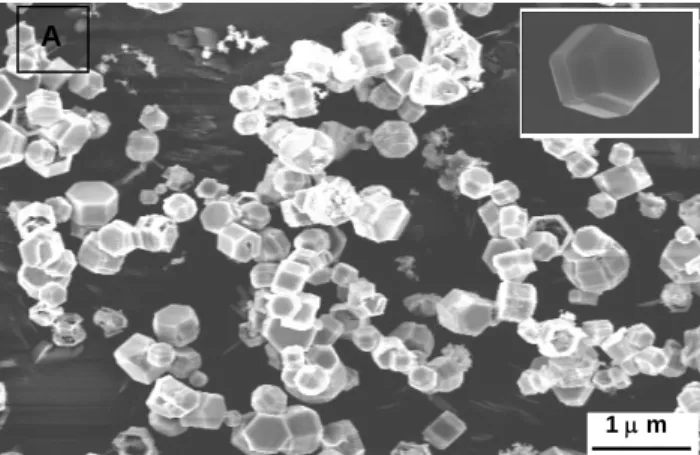
實濺鍍法可製成 CdSe 微晶析出的薄膜。
圖 1 不同 N2O 摻雜之表面粗糙度變化。 圖 2 不同 N2O 摻雜之 n&k 曲線。 圖 3 不同 N2O 摻雜之硬度。 200 300 400 500 600 700 800 900 0 1000000 2000000 3000000 4000000 5000000 6000000 7000000 8000000 9000000 10000000 5%,center 10%,center 5% 7.5% 12.5% 17.5% 22.5% (m -1) wavelength (nm) 圖 4(a) 不同貼靶面積、位置的吸收光譜(濺鍍 功率 150W)。 0.0 0.2 0.4 0.6 0.8 1.0 1.2 1.4 Ro u gh n e s s (n m ) Rms Ra 0 5 10 15 20 25 30 35 40 0.0 0.5 1.0 1.5 2.0 2.5 3.0 3.5 4.0 4.5 n. k N2O/Ar ratio % n k 0 5 10 15 20 25 30 35 40 85 90 95 100 105 110 115 120 125 130 135 G P a N2O/Ar ratio %200 400 600 800 0 1000000 2000000 3000000 4000000 5000000 6000000 7000000 8000000 9000000 10000000 5%,center 10%,center 5% 7.5% 12.5% 17.5% 22.5% (m -1) Wavelength (nm) 圖 4(b) 不同貼靶面積、位置的吸收光譜(濺鍍 功率 200W)。 200 300 400 500 600 700 800 900 0 2000000 4000000 6000000 8000000 10000000 5%,center 10%,center 5% 7.5% 12.5% 17.5% 22.5% (m -1) w avelength (nm ) 圖 4(c) 不同貼靶面積、位置的吸收光譜(濺鍍 功率 250W)。 400 600 800 0 1000000 2000000 3000000 4000000 5000000 (m -1) 4% 16% 32% wavelength (nm) 圖 4(d) 不同摻雜量之吸收光譜圖(溶膠-凝膠法 製靶)。 500 550 600 650 700 750 0 1000 2000 3000 4000 5000 6000 7000 586 nm 569 nm EM wavelength (nm ) 150W 200W 250W 圖 5(a) 貼靶濺鍍 5%之 PL 光譜。 550 600 650 700 750 400 600 800 1000 1200 1400 1600 1800 2000 2200 620 nm 596 nm E M wavelength (nm ) 150W 200W 250W 圖 5(b) 貼靶濺鍍 7.5%之 PL 光譜。 550 600 650 700 750 400 500 600 700 800 900 1000 1100 1200 1300 1400 1500 1600 1700 1800 1900 2000 2100 2200 2300 709 nm E M wavelength (nm) 150W 200W 250W 圖 5(c) 貼靶濺鍍 12.5%之 PL 光譜。 500 550 600 650 700 750 0 500 1000 1500 2000 2500 3000 3500 4000 4500 574 nm 608 nm 561 nm EM wavelength (nm) 4% 16% 32% 圖 5(d) 不同摻雜量之 PL 光譜(溶膠-凝膠法製 靶)。
12
圖 6(a) 貼靶濺鍍 7.5%之微晶玻璃試片之
TEM 影像。
圖 6(b) 貼靶濺鍍 7.5%之微晶玻璃試片之
TEM 繞射影像。
子計畫:奈米結構氧化物光子晶體材料製
程與光電特性研究
A novel hierarchical polygon prismatic nano-structure of hexagonal ZnO and Zn has been successfully grown on silicon by thermal vapor transport and condensation method. Thus, in this work, the organic solvent with zinc chemical compound was first coated and used as seeds on the silicon substrate. Subsequently, it was grown by thermal vapor transport with ZnO powder at 250°C (substrate) in Ar atmosphere. The samples were characterized using X-ray diffraction, scanning and transmission electron microscopy, and photoluminescence spectroscopy. The as-synthesized ZnO polygon prismatic nano-structure consisted of hexagonal metallic nuclei (Zn) covered with an oxidation outer thin film (ZnO). Depending on the different annealing temperature and reaction atmosphere, Zn polygon prismatic structure having various morphologies can be developed. The dimension and crystal phase can be controlled by temperature, time, kinetic surface energy, and capping molecules. The possible formation mechanism for the Zn-ZnO polygon prismatic crystal structure is identified and proposed as the Zn-ZnO mineral
bridge mechanism. Although the present
non-prefect Zn-ZnO polygon prismatic structure shows weakly UV emission and strongly deep-level emission, the PL properties and crystallization of Zn-ZnO prismatic nanocrystals could be improved by suitable post-treatment
Figure 1 shows typical scanning electron microcopy (SEM) and TEM image of the Zn polygon prismatic crystals. The diameter of the crystals can be tuned from 30 nm to 2m by increasing the concentration of the Zn(ClO4)2 solution. As the concentration of the Zn(ClO4)2 solution increases, the amount of Zn particles would increase. The Zn particles behave as the nucleus sites of the larger Zn crystals. The amount of Zn nucleus sites would be proportional to the concentration of the Zn(ClO4)2 solution. In the highly concentration solution, the large and sharp Zn polygon prismatic crystals (~2m) were synthesized on the substrate by thermal vapor process (Fig. 1A). On the contrary, as the amount of nucleus sites decreases, the crystal size of Zn polygon prismatic structure shrinks to ~30 nm scale (Fig. 1C). Figure 2A illustrates the schematic mechanism of such a process. In this case, the initial nucleus sites were prepared by Zn(ClO4)2 solution. When Zn sources were transported by thermal evaporation process, these nucleus sites would cap these Zn molecules to develop the nanocrystals. In the following step, some of the fine Zn nanocrystals would get together to form the large crystals. According to above statement, it was found that the concentration of the Zn(ClO4)2 solution could determine the nucleus sites. Therefore, the amount of nucleus sites would determine the size of the Zn polygon prismatic crystals. It was found that the initial nuclei of Zn polygon prismatic crystals were emerged into the small Zn polygon prismatic crystals by themselves and its diameter is less than 10 nm, as seen in Fig. 2B. Figure 2C shows the special distribution pattern of Zn polygon prismatic nanocrystals (~30 nm) formed in the initial stage of crystal growth. The spreading region of these distributed Zn nanocrystals has diameter around 150 nm that is close to the composing-crystals obtained in our experiments (Fig. 2D). It suggests that the spatial distribution region of Zn nanocrystals would develop the base for the larger size crystals. After the suitable growth time, the Zn polygon prismatic crystals will be formed on that base (Fig. 2E).
The shape of the Zn polygon prismatic nanocrystals would vary with the growth time. Figure 3 presents the growth of the Zn polygon prismatic nanocrystals as a function of time. The prefect Zn nanocrystals are observed for the growth time of 2 hours. When the growth time exceeds 2 hours, the shape of the Zn polygon
prismatic nanocrystals would begin to
disintegrate (Fig. 3B). It is well known that metal state will become unstable when the temperature
13 reaches around its melting point. The apparent melting point (Zn: mp 410˚C) would be reduced for nanocrystal with size small enough. The balance between the thermodynamic and kinetics would be influenced by the growth time. It implies that if the growth time exceeds the critical time, the equilibrium status would be destroyed. It could be due to the unstable lattice-site of zinc atom in the Zn polygon prismatic crystals, long time thermal heating will make the crystal structure destructible. To keep the stability of grown crystals, the oxidation treatment to modify the surface status of Zn polygon prismatic crystal is applied. Both Zn and ZnO have the hexagonal (hcp) structure. From the growth kinetics point of view, when ZnO is formed, rearrangement of the sublattices of zinc from hcp (Zn) to hcp (ZnO) has to occur only at Zn reaction front. Therefore, the nucleating ZnO grain has a template to follow the orientation of Zn exactly. Figure 4 shows the surface
morphology of Zn polygon prismatic
nanocrystals after thermal treatment at 550˚C for 3 hours. It is obvious that Zn polygon prismatic crystals with surface treatment could retain the complete crystals structure (Figure 4B). It is due to the ZnO layer formed by surface treatment that prohibits the zinc atoms leaving away lattice and prevents the crystals from being destroyed.
Figure 5 shows the X-ray diffraction (XRD) spectrum of the nanostructures, where the intensity of zinc crystalline phase is different for
different treatment. In contrast with
crystallization of Zn polygon prismatic
nanocrystals, the sample that undergoes the oxidation treatment presents the stronger XRD peak intensity than the other. For the Zn polygon prismatic nanocrystals subjected to oxidation treatment on Zn surface, the ZnO crystalline phase can be developed as identified from the
XRD (Fig. 5B). Chemical composition
microanalysis by energy-dispersive spectrometry (EDS) reveals that the Zn polygon prismatic nanocrystals with surface oxidation are composed of more content of zinc compared to those without surface treatment (with an atomic ratio of = 15:1). This is in a good agreement with the XRD analysis result.
The photoluminescence (PL) measurements of the synthesized Zn polygon prismatic nanocrystals are performed at room temperature, using a He-Cd laser line of 325 nm as the excitation source. As shown in Figure 6, UV and green emission with peaks at 380 nm and 530 nm are observed for the Zn polygon prismatic nanocrystals with surface treatment. The PL spectrum is different from that of Zn. Zn polygon
prismatic nanocrystals without oxidation
treatment. No emission peak is found because the Zn polygon prismatic nanocrystal is only composed by pure zinc metal in this case. On the contrary, as the Zn nanocrystals have undergone oxidation treatment, the surface will form a thin oxide layer. According to the XRD analysis, the oxide layer is basical zinc oxide. ZnO usually
displays two major PL peaks, UV
(near-band-edge) emission peak and green (or red) emission peak (deep-level). The deep-level emissions are generally associated with defects in
ZnO lattice. Besides, the near-band-edge
transition could not effectively exist in the non-crystalline ZnO. Although the developed Zn
polygon prismatic nanocrystals are well
crystalline, the interface between Zn and ZnO surface layer usually results in large lattice mismatch (17%). The kind of interface becomes the defect generator to support the deep-level emissions. In addition to lattice mismatch, the incomplete oxidation of zinc produces the defects inside surface layer and gives deep-level emission too. A 1 m B 200 nm C
14 Fig. 1. SEM images of the Zn polygon prismatic crystals synthesized by liquid solution and vapor transport method. A) Zn polygon prismatic crystals of 2-μm diameter. B) Zn polygon prismatic crystals of 300-nm diameter. C) TEM images of the Zn polygon prismatic nanocrystals of 30-nm diameter.
Fig.2. (A) Schematic illustration of growth mechanism of Zn polygon prismatic nanocrystals. (B) TEM image of the nuclei of Zn polygon prismatic nanocrystals (~7 nm) (C) TEM image of Zn polygon prismatic nanocrystals (30 nm) formed by thermal vapor process. (D) Growing Zn polygon prismatic nanocrystals (0.6μm). (E) SEM image of Zn polygon prismatic crystals (0.7 μm) formed by the collection of the ultra-fine Zn nanocrystals.
Fig. 3. SEM images of Zn polygon prismatic nanocrystals growing as a function of time. (A) 2 hours. (B) more than 3 hours.
150 nm 15 0 30 nm 20 0 11 0 100 010 010 11 0 (100) (010) ( 1 ( 1 ( 1 ( 0 1 m A B 1 m B A 500 nm A B B A
350 400 450 500 550 600 650 P L int en s ity ( a. u. ) 380 W avelength (nm) Zn nanocrystals ZnO /Zn nanocrystals
Fig. 4. SEM images of Zn polygon prismatic nanocrystals were thermally heated at 550˚C and kept for 3 hours (A) without and (B) with oxidation treatment.
Fig. 5. X-ray diffraction (XRD) spectrum of Zn polygon prismatic nanocrystals were thermally heated at 550˚C and kept for 3 hours (A) without and (B) with oxidation treatment.
Fig. 6. Room-temperature photoluminescence spectra recorded from Zn polygon prismatic nanocrystals with and without oxidation treatment.
子計畫:各種型態之奈米碳基材料開發及場發射元件之製作
2 0 3 0 4 0 5 0 6 0 Z n (0 0 2 ) Z n (1 0 2 ) Z n (1 0 1 ) Z n (1 0 0 ) 2 C ou n t A 2 5 3 0 3 5 4 0 4 5 5 0 5 5 6 0 Z n (1 02 ) Z n (10 1) Z n (10 0 ) Z n (0 02 ) Z n O (1 02 ) Z n O (11 0 ) Z n O (10 1 ) Z n O (1 00 ) Z n O (00 2 ) C o u n t 2 B16