262 IEEE ELECTRON DEVICE LETTERS, VOL. 27, NO. 4, APRIL 2006
Improvement of Electrical Characteristics
for Fluorine-Ion-Implanted
Poly-Si TFTs Using ELC
Chun-Hao Tu, Ting-Chang Chang, Po-Tsun Liu, Che-Yu Yang, Hsin-Chou Liu,
Wei-Ren Chen, Yung-Chun Wu, and Chun-Yen Chang, Life Fellow, IEEE
Abstract—The fluorine ion implantation applied to the
polycrys-talline silicon thin-film transistors (poly-Si TFTs) is investigated in this letter. Experimental results have shown that fluorine ion implantation effectively minimized the trap state density, lead-ing to superior electrical characteristics such as high field-effect mobility, low threshold voltage, and highON/OFF current ratio. Furthermore, the fluorine ions tended to segregate at the interface between the gate oxide and poly-Si layers during the excimer laser annealing, even without the extra deposition of pad oxide on the poly-Si film. The presence of fluorine obviously enhanced electrical reliability of poly-Si TFTs.
Index Terms—Fluorine ion implantation, polycrystalline silicon
thin-film transistors (poly-Si TFTs).
I. INTRODUCTION
T
HE EXCIMER laser crystallization (ELC) method is widely adopted in the thin-film transistor–liquid crystal display (TFT–LCD) industries for fabricating high-quality polysilicon films with very few in-grain defects [1], [2]. The un-desirable leakage current, however, has been the main issue for the application of ELC to polycrystalline silicon TFTs (poly-Si TFTs). To address the issue, the defect passivation method was proposed in the poly-Si TFT manufactures. The hydrogen plasma treatment was the widely used method to passivate the trap states at the grain boundaries [3], but it is not easy to control the hydrogen concentration in the poly-Si films. The formed Si–H bonds after hydrogen plasma treatment are not effectively immune against the impact of driving current, and thereby alternative technologies should be developed further. The fluorine-ion-incorporation technology has been applied in many electronic manufactures such as the improvement of Si/SiO2 interface hardness against the hot carrier impactManuscript received November 28, 2005; revised January 11, 2006. This work was supported in part by the National Science Council of China under Contracts NSC94-2215-E009-063, NSC94-2215-E009-031, and NSC94-2120-M-110-005, in part by ChungHwa Picture Tubes, Ltd. (CPT), and in part by MOEA Technology Development for Academia under Project 94-EC-17-A-07-S1-046. The review of this letter was arranged by Editor J. Sin.
C.-H. Tu, C.-Y. Yang, H.-C. Liu, W.-R. Chen, Y.-C. Wu, and C.-Y. Chang are with the Institute of Electronics, National Chiao-Tung University, Hsinchu 300, Taiwan, R.O.C.
T.-C. Chang is with the Department of Physics and Institute of Electro-Optical Engineering, National Sun Yat-Sen University, Kaohsiung 804, Taiwan, R.O.C. and also with the National Nano Device Laboratories, Hsinchu 300, Taiwan, R.O.C. (e-mail: [email protected]).
P.-T. Liu is with the Department of Photonics and Display Institute, National Chiao-Tung University, Hsinchu 300, Taiwan, R.O.C.
Digital Object Identifier 10.1109/LED.2006.870420
[4]–[7], the enhanced breakdown voltage of device, and the passivation of trap centers. In previous studies [8], [9] on the fluorine-implanted poly-Si TFTs, the formed Si–F bond can eliminate the trap state density to obtain higher field-effect mobility, superior electrical reliability, and lower threshold voltage for n-channel TFTs. However, the prior art needed additional pad oxide deposition during TFT fabrication, leading to a complex process.
In this letter, a new manufacture method using fluorine ion implantation for poly-Si TFTs was proposed. The proposed process is simple and does not need additional pad oxide deposition. The electrical characteristics of the proposed poly-Si TFT will be reported in this letter, including theI−V transfer curves and direct current (dc) stress reliability.
II. EXPERIMENTAL
A 50-nm-thick undoped amorphous silicon (a-Si) layer was deposited on a 500-nm-thick oxide-coated silicon wafer by low-pressure chemical vapor deposition (LPCVD) system. Then, the fluorine ion implantation was performed to the a-Si layer. The ion implantation dose was5 × 1013cm−2with an accelerating energy of 11 keV. The recrystallization procedure was realized by a KrF excimer laser with an energy density of 300 mJ/cm2 under a vacuum ambient (∼ 10−3 torr) at room temperature. After the crystallization of the a-Si layer, the silicon-active regions were patterned by photolithography and etch processes. The tetraethylorthosilicate (TEOS) precursor was used for the formation of the gate dielectric and was performed by the LPCVD system at 700◦C. The poly-Si gate was also deposited by the LPCVD system. After the poly-Si gate pad definition, the P31+ion implantation was implemented as the source–drain regions. The activation of the source–drain regions was realized by the thermal budget of the passivation TEOS oxide layer deposited at 700◦C for 3 h. The contact holes were then defined and etched by the buffer oxide etching (BOE) solution. The aluminum layer was deposited, defined, and etched to form the metal pads. Finally, the finished poly-Si TFT devices were sintered in a thermal furnace at 350◦C for 30 min.
III. RESULTS ANDDISCUSSION
Fig. 1 shows the secondary ion mass spectrometry (SIMS) depth profile of the fluorine-implanted a-Si/buffer oxide struc-ture after ELC. The inset is the cross section of the proposed
TU et al.: IMPROVEMENT OF ELECTRICAL CHARACTERISTICS FOR FLUORINE-ION-IMPLANTED POLY-Si TFT 263
Fig. 1. SIMS depth profile of fluorine in the poly-Si channel/buffer oxide structure. The inset plot shows the cross section of fluorine-ion-incorporated poly-Si TFTs.
Fig. 2. Comparison ofID−VG characteristics for conventional TFTs and fluorine-ion-implanted TFTs (W/L = 10 µm/10 µm and VD= 0.1 V).
poly-Si TFT device. It is observed that a high level of fluorine concentration is present at the surface of the poly-Si film and at the interface between the poly-Si and buffer oxide layers. The fluorine ions tended to pile up at the interface between the poly-Si and SiO2layers, whereas the implantation project range targeted the middle of the a-Si layer. Compared with previous studies, in this letter, the high concentration of flu-orine ions at the poly-Si interface is still observed after the crystallization process, even without extra deposition of the pad oxide layer on the a-Si layer. This indicates that the fluorine ions diffused into the oxidized surface of the a-Si layer in the excimer laser annealing step. During the ELC process, the fluorine ions segregated at the oxidized surface of the poly-Si film and at the interface between the poly-poly-Si and buffer oxide layers. Based on a previous study [10], the fluorine ions were also found to segregate in the oxide layer during excimer laser annealing. The high concentration of fluorine ions at the poly-Si surface and at the interface between the poly-Si and buffer oxide layers was capable of eliminating the
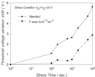
Fig. 3. Threshold voltage variation versus stress time for the conventional TFT and the fluorine-implanted TFT.
Fig. 4. On-current degradation versus stress time for the conventional TFT and the fluorine-implanted TFT.
strain bonds in the poly-Si during the excimer laser annealing [10]. In this letter, we have confirmed that the fluorine ions moved toward the poly-Si interface because of the sequent postimplant thermal annealing, even without any pad oxide deposition. The fluorine ions passivated the strain bonds and the dangling bonds in the poly-Si film, leading to the enhanced electrical characteristics. The electrical characteristics of the fluorine-ion-implanted poly-Si TFTs were also investigated in this letter. The ID−VG transfer characteristics are shown in Fig. 2. The key parameters were summarized in the inset table in Fig. 2. It was found that the electrical characteristics of the poly-Si TFT were improved effectively by the implementation of fluorine ion implantation. The fluorine-incorporated poly-Si TFTs exhibited higher field-effect mobility, higherON/OFF
current ratio, lower trap state density, superior subthreshold swings, and lower threshold voltage for n-channel poly-Si TFTs with an implantation dose of5 × 1013cm−2.
The dc voltages were applied to the devices for the study of electrical reliability. The stress condition was set atVD= VG= 20 V, and the stress times were 100, 200, 600, 1000, 2000,
264 IEEE ELECTRON DEVICE LETTERS, VOL. 27, NO. 4, APRIL 2006
6000, and 10 000 s. The threshold voltage variations and the on-current degradation that resulted from the broken Si–Si and Si–H bonds during the electrical operation [11], [12] are shown in Figs. 3 and 4, respectively. It was found that the poly-Si TFTs without fluorine implantation gained the maximum ∆VTH and ∆ION/ION after dc stress. The Si–Si and Si–H bonds suffered from serious hot carrier stress, causing the largest ∆VTH and∆ION/ION. In contrast, the fluorine-incorporated
poly-Si TFT has high immunity against the hot carrier stress and thereby exhibited minimum ∆VTH and ∆ION/ION as compared to a typical poly-Si TFT. Therefore, the significant improvement in the electrical reliability can be attributed to the formation of stronger Si–F bonds in place of weaker Si–Si and Si–H bonds in the poly-Si.
IV. CONCLUSION
We have successfully demonstrated the fluorine-incorporated poly-Si TFTs in this letter. The field-effect mobility for fluorine-implanted poly-Si TFTs was twice as large as that of the conventional poly-Si TFT using the ELC method. The improvement of threshold voltage was from 3.07 to 1.19 V with the incorporation of fluorine ions. In addition, the fluorine-incorporated poly-Si TFTs can possess higher hot carrier endurance. This is presumably due to the formation of stronger Si–F bonds instead of the weak Si–Si and Si–H bonds in the poly-Si layer. Furthermore, the manufacturing process is simple and compatible with the conventional poly-Si TFT fabrication processes.
REFERENCES
[1] T. Sameshima, S. Usui, and M. Sekiya, “XeCl excimer laser annealing used in the fabrication of poly-Si TFT’s,” IEEE Electron Device Lett., vol. EDL-7, no. 5, pp. 276–278, May 1986.
[2] M. Miyasaka and J. Stoemenos, “Excimer laser annealing of amorphous and solid-phase-crystallized silicon films,” J. Appl. Phys., vol. 86, no. 10, pp. 5556–5565, Nov. 1999.
[3] I. W. Wu, A. G. Lewis, T. Y. Huang, and A. Chiang, “Passivation kinetics of two types of defects in polysilicon TFT by plasma hydrogenation,”
IEEE Electron Device Lett., vol. 12, no. 4, pp. 181–183, 1993.
[4] Y. Nishioka, Y. Ohji, K. Mukai, T. Sugano, Y. Wang, and T. P. Ma, “Dielectric characteristics of fluorinated ultradry SiO2,” Appl. Phys. Lett., vol. 54, no. 12, pp. 1127–1129, Mar. 1989.
[5] Y. Nishioka, K. Ohyu, Y. Ohji, N. Natuaki, K. Mukai, and T. P. Ma, “Hot-electron hardened Si-gate MOSFET utilizing F implantation,” IEEE
Electron Device Lett., vol. 10, no. 4, pp. 141–143, Apr. 1989.
[6] Y. Nishioka, K. Ohyu, Y. Ohji, and T. P. Ma, “Channel length and width dependence of hot-carrier hardness in fluorinated MOSFET’s,” IEEE
Electron Device Lett., vol. 10, no. 12, pp. 540–542, Dec. 1989.
[7] P. J. Wright and K. C. Saraswat, “The effect of fluorine in silicon dioxide gate dielectrics,” IEEE Trans. Electron Devices, vol. 36, no. 5, pp. 879– 889, May 1989.
[8] H. N. Chern, C. L. Lee, and T. F. Lei, “The effects of fluorine passivation on polysilicon thin-film transistors,” IEEE Trans. Electron Device, vol. 41, no. 5, pp. 698–702, May 1994.
[9] J. W. Park, B. T. Ahn, and K. Lee, “Effects of F implantation on the characteristics of poly-Si films and low-temperature n-ch poly-Si thin-film transistors,” Jpn. J. Appl. Phys. 1, Regul. Rap. Short Notes, vol. 34, no. 3, pp. 1436–1441, Mar. 1995.
[10] C. L. Fan and M. C. Chen, “Performance improvement of excimer laser annealed poly-Si TFTs using fluorine ion implantation,” Electrochem.
Solid-State Lett., vol. 5, no. 8, pp. 75–77, Mar. 2002.
[11] S. Banerjee, R. Sundaresan, H. Shichijo, and S. Malhi, “Hot-electron degradation of n-channel polysilicon MOSFET’s,” IEEE Trans. Electron
Devices, vol. 35, no. 2, pp. 152–157, Feb. 1988.
[12] M. Hack, A. G. Lewis, and I. W. Wu, “Physical models for degradation effects in polysilicon thin-film transistors,” IEEE Trans. Electron Devices, vol. 40, no. 5, pp. 890–897, May 1993.