This content has been downloaded from IOPscience. Please scroll down to see the full text.
Download details:
IP Address: 140.113.38.11
This content was downloaded on 25/04/2014 at 03:52
Please note that terms and conditions apply.
The influences of device geometry and p-type doping on a solution-processed polymer
space-charge-limited transistor
View the table of contents for this issue, or go to the journal homepage for more 2010 J. Phys. D: Appl. Phys. 43 205101
(http://iopscience.iop.org/0022-3727/43/20/205101)
J. Phys. D: Appl. Phys. 43 (2010) 205101 (6pp) doi:10.1088/0022-3727/43/20/205101
The influences of device geometry and
p-type doping on a solution-processed
polymer space-charge-limited transistor
Yu-Chiang Chao
1, Chun-Yu Chen
1, Hsiao-Wen Zan
2,3and
Hsin-Fei Meng
1,31Institute of Physics, National Chiao Tung University, Hsinchu 300, Taiwan 2Deparment of Photonics, National Chiao Tung University, Hsinchu 300, Taiwan E-mail:[email protected]@mail.nctu.edu.tw
Received 17 December 2009, in final form 25 March 2010 Published 4 May 2010
Online atstacks.iop.org/JPhysD/43/205101 Abstract
A polymer vertical transistor with an on/off current ratio higher than 104is demonstrated. The proposed space-charge limited transistor (SCLT) uses a metal-grid base containing
high-density submicrometre openings to modulate the vertical space-charge-limited current (SCLC). The key to obtaining a high on/off current ratio is to reduce the leakage current of SCLT. In this paper, an improved device structure that isolates the grid metal by using both top and bottom insulating layers is demonstrated. Then, with an identical proposed structure, the geometric design is also found to significantly influence the on/off ratio over 3 orders of magnitude. The competition between the SCLC and the grid to collector leakage current is analysed. Finally, the influence of tetrafluoro-tetracyano-quinodimethane doping on the transistor characteristics is investigated. The results are important for the design of polymer vertical transistors with high on/off ratios.
(Some figures in this article are in colour only in the electronic version)
1. Introduction
Polymer transistors have been studied extensively due to their applications on low-cost large-area transistor arrays or on flexible electronics. A conventional polymer field-effect transistor (FET) is a horizontal device with source and drain electrodes in the same plane. Low mobility conjugated polymers and long channel length seriously limit the performance of the polymer FET. As a result, the polymer FET usually exhibits high operation voltage and low operation frequency. To circumvent these limitations, polymers with high mobility are synthesized [1,2] and various vertical transistors with short channel length perpendicular to the substrate are proposed [3–14]. However, even with high turn-on current under low operatiturn-on voltage, the turn-on/off current ratio for most vertical transistors is as low as a few hundred. The off current control is a key issue for the development of vertical transistors.
3Authors to whom any correspondence should be addressed.
In our previous reports, a vertical space-charge-limited transistor (SCLT) with high turn-on current density is demonstrated [11,12]. Analysis for reducing its off current density is given below. The SCLT functions similarly to the vacuum tube triode, the carriers are injected from the emitter into the semiconductor, passing through the openings on the metal-grid base and finally arriving at the collector. The on and off states of the SCLT are determined by whether carriers encounter a potential barrier between emitter and collector or not. The magnitude of the potential barrier is controlled by the voltages of grid and collector. The potential at the centre of the opening is expressed by a linear combination of grid and collector voltages as λVGE+ VCE [15], the factor λ
depends on the device geometry. The minimum off current density comes from the competition of two current sources, they are the current density from emitter to collector JC1
and the leakage current density from grid to collector JC2,
as indicated in figure 1(a). Theoretically, for a fixed VCE,
J. Phys. D: Appl. Phys. 43 (2010) 205101 Y-C Chao et al
Figure 1. (a) The schematic device structure. Two transistor off current sources are indicated. JC1is the current density from emitter to collector, while JC2is the leakage current density from grid to collector. (b) The schematic curves of the transistor off current as a function of VGunder various conditions. Red dotted lines represent
JC1for the devices with different λ, while blue dashed lines represent JC2for the devices with or without Al2O3on grid. The black curve (i) demonstrates the total JCas a sum of JC1and JC2for devices with low λ and without Al2O3on grid, while the black curve (ii) demonstrates the JCfor devices with high λ and with Al2O3on grid. (Colour online.)
barrier (that is by increasing the VGE) to reduce JC1, as shown in
figure1(b). However, when JC1decreases with increasing VGE, JC2increases due to the increasing voltage drop between grid
and collector. In previous reports, including for our SCLT and the static-induction transistor (SIT) reported by Kudo et al [10],
JC2is large because the grid is only blocked by the Schottky
barrier between the grid metal and the organic semiconductor. As a result, an insulating layer surrounding the grid metal is essential to reduce JC2. Besides, better grid control on the
potential barrier is beneficial for reducing JC1. For a fixed VCE, higher λ represents better grid control on the potential
barrier. In a device with high λ, a small increase in VGE will
cause JC1 to decrease dramatically, as shown in figure 1(b).
For this reason, optimizing the device geometric structure to maximize λ is also needed for increasing the grid control on the potential barrier and hence reducing JC1. Therefore, adding an
insulating layer surrounding the grid metal and optimizing the device geometric structure are both essential to reduce the off current of the transistor and hence increase the on/off ratio of the SCLT, as indicated by the black curves (ii) in figure1(b).
In this paper, we present a SCLT with an insulating polymer between Al grid and emitter, and an O2plasma grown
Al2O3 layer on top of the Al grid. The operating voltage is
as low as 2 V, output current density is 5.15 mA cm−2 and the on/off ratio is as high as 10775. The on/off ratio is two orders of magnitude higher than those in previous results [3–
14]. In our experiment, we also found a strong dependence
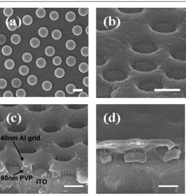
Figure 2. SEM images with 0.2 µm white scale bar. (a) Top view of two-dimensional colloidal arrays on PVP. (b) The 400 Å Al grid with random 2000 Å openings on PVP. (c) Openings form at sites without Al grid. (d) Device image before Al collector deposition. The thickness of P3HT is 1338 Å, Al grid is 400 Å and PVP is 600 Å. (Colour online.)
between device geometry and device performance to support the above analysis. Changing the thickness of Al grid metal and the thickness of P3HT layer considerably influences the on/off current ratio. The influence of controllable tetrafluoro-tetracyano-quinodimethane (F4-TCNQ) doping on the transistor characteristics is studied to demonstrate the dopant screening effect. The optimized SCLT is demonstrated by using the non-photolithography method. Since the emitter– collector distance is shorter than the channel length in horizontal polymer FET, high current output and high speed can be achieved even for relatively low carrier mobility materials. Besides, the fabrication procedure is simpler than FET as no photolithography is needed. Furthermore, since the current of SCLT is uniformly distributed in the bulk, SCLT is free from the unpredictable conditions at the dielectric interface in FET. The proposed high on/off ratio SCLT can easily be applied to flexible and low-cost array applications.
2. Experimental
The schematic device structure of SCLT and scanning electron microscopy (SEM) images of each device fabrication stage are shown in figures 1(a) and 2. The device is fabricated on an indium-tin-oxide (ITO) glass substrate. After flatten-ing the ITO surface with 150 W O2 plasma for 30 min, the
cross-linkable poly(4-vinyl phenol) (PVP) is spin coated on the ITO substrate to form the 600 Å PVP layer and then an-nealed at 200◦C for 60 min in vacuum. The cross-linkable PVP solution consists of 3 wt% PVP polymer (Aldrich,
Mw∼ 20 000), 1.1 wt% poly(melamine-co-formaldehyde)
methylated (Aldrich, Mw∼ 511) as a cross-linking agent and
propylene glycol monomethyl ether acetate as a solvent. After treating the PVP surface with 50 W O2plasma for 5 s to turn the
PVP surface into hydrophilic, the substrate is submerged into 2000 Å positively charged polystyrene spheres (Merck, K6-020) dilute ethanol solution with 0.8 wt% for 3 min and then transferred into a beaker with boiling isopropanol solution for 10 s. The substrate is immediately blown dry in a unidirec-tional nitrogen flow to form two-dimensional colloidal arrays without aggregation as shown in figure2(a). Then, Al with dif-ferent thicknesses from 200 to 800 Å is evaporated as grid with polystyrene spheres as shadow mask, the polystyrene spheres are removed by an adhesive tape (Scotch, 3M). Figure 2(b) shows the SEM image of Al grid with random 2000 Å openings on PVP. The substrate is then treated with 150 W O2plasma
for 10 min to remove PVP at sites without Al grid coverage. After O2plasma treatment, ITO is disclosed to serve as emitter
as shown in figure2(c). An Al2O3layer on top of the Al grid
is also formed after O2plasma treatment [16] which prevents
current flow from Al grid to collector. P3HT with different thicknesses is then spin coated from 2.5 wt% chlorobenzene solution at 600, 1000, 1500, 2000, 3000 and 7000 rpm. The thickness of P3HT is determined to be 1794, 1338, 1081, 1011, 678 and 480 Å by measuring another O2 plasma treated ITO
glass with P3HT spin coated at the same spin speed. Alu-minium collector is finally deposited to complete the SCLT with an active area of 1 mm2. Figure2(d) shows the SEM im-age of the device before Al collector deposition. It is observed that the cross-linked PVP keeps its conformation without being dissolved by chlorobenzene. The P3HT surface is not totally flat, sinks can be found at the position of openings. The depth of the sink depends on the thickness of grid, PVP and P3HT. Its influence on the device performance will be discussed later. To study the doping effect, the dopant F4-TCNQ is utilized to dope P3HT and poly(9,9-di-n-octylfluorene-alt-(1,4-phenylene-((4-sec-butylphenly)-imino)-1,4-phenylene)) (TFB). The thick-ness of TFB is 1200 Å which is prepared from 2 wt% xy-lene solution. The F4-TCNQ dopant is blended with poly-mer at various percentages. SEM images are obtained with a field-emission scanning electron microscopy (JEOL JSM-7401). Transistor characteristics are recorded using an Agilent E5270B modular parameter analyzer.
3. Results and discussion
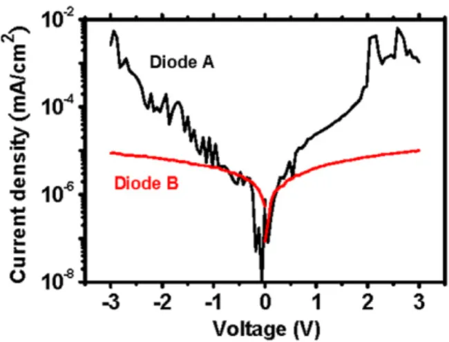
The influence of the existence of Al2O3 on Al grid is
demonstrated by comparing current density–voltage curves of two diodes. Diode A has the structure Al/P3HT/Al and diode B has the structure Al/Al2O3/P3HT/Al. For diode B, the Al2O3
on the Al electrode bellow P3HT is grown by 150 W O2plasma
treatment for 10 min. The thickness of P3HT is 1000 Å for both diodes. As shown in figure3, the current of diode A is higher than that of diode B. The existence of Al2O3 indeed helps
reduce the leakage current. Because it has been demonstrated that O2plasma treatment on Al film of no longer than 15 min
will not cause an Al2O3 layer thicker than 50 Å [16,17], the
thickness of Al2O3on Al grid in our work is believed to be in
the range between 50 and 100 Å. Since the thickness of Al grid
Figure 3. J –V curves of diodes in the structure Al/P3HT/Al (diode A) and Al/Al2O3/P3HT/Al (diode B). (Colour online.)
Figure 4. (a) Collector current density and (b) grid current density in absolute value as a function of collector voltage at various grid voltages of the device with 2000 Å opening on Al grid. The On/off ratio of 10775 is obtained at VC= −2 V. The inset in (a) shows emitter–collector diode characteristics. The inset in (b) shows the value of the grid current density as a function of collector voltage. (Colour online.)
is 4–8 times larger than 50 Å, the influence of the Al2O3layer
on the electrical characteristics of Al grid is not significant. The optimal transistor characteristics of polymer SCLT with opening diameter of 2000 Å on Al grid are shown in figure 4. The thicknesses of Al grid and P3HT are 400 Å and 1338 Å, respectively. The PVP film exhibits good insulating property without breakdown in the voltage
J. Phys. D: Appl. Phys. 43 (2010) 205101 Y-C Chao et al
range from −2 to 2 V. Leakage current in ITO/PVP/Al is around 0.0003 mA cm−2at 2 V. The ITO emitter is commonly grounded and the Al collector is negatively biased at VCE.
Negative collector current density (JC) means that holes are
driven towards the collector through the grid. The definition of the on/off ratio is JC(VGE = −1 V) divided by JC(VGE =
2.3 V). Figure 4(a) demonstrates an apparent modulation of
JCby VGEfrom−1 to 2.3 V. The on/off ratio is 763 as VCEis
−1 V, 6143 as VCEis−1.5 V and 10775 as VCE is−2 V. The
magnitude of the on/off ratio around 104is two orders higher
than those in previous reports. Insulating layers surrounding Al grid indeed allow a high VGE(2.3 V) to turn off the transistor
while keeping JG still low as shown in figure 4(b) and the
inset in figure 4(b). When VCE is −2 V and VGE is −1 V,
the transistor output current density is 5.15 mA cm−2 and the current gain (JCE/JGE) of the transistor is around 104. The inset
in figure4(a) is the J –V curve of the emitter–collector diode (ITO/P3HT/Al) without applying voltage on the grid. This curve is similar to that of transistor electronic characteristics in on state, which confirms our assumption that the function of Al grid is to modulate the vertical space-charge-limited current (SCLC) in ITO/P3HT/Al diode. Transistor characteristics better than previously reported [10] may come from many aspects. First, the Al2O3 on top of the Al grid reduces the
leakage current from grid to collector and hence reduces the transistor off current and increases the on/off ratio. Second, the distance between Al grid and emitter is only 600 Å which facilitates the grid control on the potential barrier between emitter and opening, and hence results in a high on/off ratio.
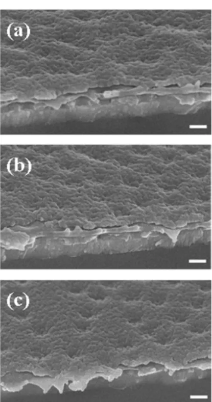
The improvement of the grid control on the potential barrier can be further investigated as follows. It was reported in previous studies that the grid control was enhanced by substituting the grid electrode with 2000 Å openings [8,10] for the grid electrode with 1 µm gaps [9]. In this study, we found that the device geometry also plays an important role in influencing the grid control and hence the device on/off ratio. As shown in the SEM images in figure5, sinks can be observed on the P3HT surface at the positions of openings. It is found that the depth of sinks, which is determined by the thickness of Al grid, PVP and P3HT, is strongly related to the device on/off ratio. The underlying mechanisms can be explained as follows. For the potential at the centre of the opening expressed by λVGE+ VCE, the geometric factor λ
is proportional to the device on/off ratio and is dependent on the depth of sinks. When the depth of sinks is small (shallow sinks), collector metal is well above the channel. Carriers from emitter to collector pass through openings surrounded by grid. Grid potential strongly influences carrier transport, λ is large and the device exhibits a high on/off ratio. When the depth of sinks is large (deep sinks), the distance between emitter and collector in the centre of the openings is short and the collector inserts into the region surrounded by the grid. Carriers passing through the centre of the openings arrive at the collector before encountering the grid potential field. As a result, λ is small. Moreover, deep sinks usually reduce the P3HT film thickness at grid corners and therefore produce a leakage path between grid and collector. The device on/off ratio becomes poor. The following experiments reveal the proposed geometry effect.
Figure 5. SEM images of devices with sinks on the collector surface. The thickness of PVP is 600 Å, while the thickness of Al grid is 400 Å. The thickness of P3HT in devices are (a) 1011 Å, (b) 678 Å, (c) 480 Å. White scale bar is 0.2 µm.
Firstly, transistors are fabricated with fixed P3HT thickness, fixed PVP thickness and various Al grid thicknesses. The Al grid thicknesses are 200, 400, 600 and 800 Å. The P3HT thickness is fixed at 1081 Å and the PVP thickness is fixed at 600 Å. On/off ratios shown in figure 6 are defined by dividing JC(VGE = −1 V) by JC(VGE = 2 V) while VCE
is fixed at−1.5 V. As shown in figure 6(a), on/off ratios of the devices with Al grid thickness in the range 400–600 Å are around 2800. For devices with 200 Å Al grid, on/off ratio is lower than 220. This is because, when carriers pass through openings, increasing Al grid thickness enhances the influence of grid potential on carriers. When Al grid thickness reaches 800 Å, deep sinks are produced because the thickness of P3HT becomes much smaller than the total thickness of Al grid and PVP. Large leakage current from Al grid to collector occurred and the on/off ratio is almost zero. Secondly, transistors with fixed Al grid thickness, fixed PVP thickness and various P3HT thicknesses are fabricated. The P3HT thicknesses are 1794, 1338, 1081, 1011, 678 and 480 Å. The Al grid thickness is fixed at 400 Å and PVP thickness is fixed at 600 Å. We choose Al grid as 400 Å rather than 600 Å to optimize the P3HT thickness so as to facilitate the process control. With 600 Å Al grid, thin P3HT at grid corner easily causes the leakage current between grid and collector. Therefore, the P3HT thickness was optimized with the device with 400 Å Al grid. When varying P3HT thicknesses as shown in figure6(b), on/off ratios of transistors with the P3HT thickness higher than 1000 Å are higher than 103. In these conditions, the thickness of P3HT is equal to or larger than the total thickness of Al grid and PVP. The highest on/off ratio is obtained for transistors with 1338 Å 4
Figure 6. On/off ratios obtained at VC= −1.5 V. (a) On/off ratios of transistors with 200, 400, 600 and 800 Å Al grid, while the P3HT thickness is fixed at 1081 Å. (b) On/off ratios of transistors with 1794, 1338, 1081, 1011 and 678 Å P3HT, while the Al grid thickness is fixed at 400 Å.
P3HT. Shallow sinks are observed on the transistor with the 1011 Å P3HT surface as shown in figure5(a). For transistors with P3HT as thin as 678 or 480 Å, deep sinks appear on the P3HT surface as shown in figures5(b) and (c). A large leakage current from Al grid to collector makes the on/off ratio almost zero. In conclusion, an optimal control of the thickness of P3HT, Al grid and PVP is necessary to obtain a high on/off ratio SCLT.
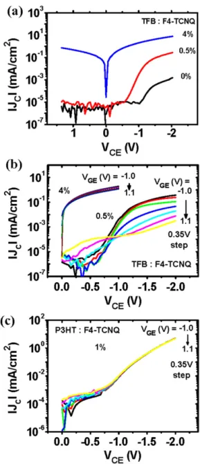
Finally, in order to demonstrate the influence of controllable doping on the transistor characteristics, the dopant F4-TCNQ, which is commonly used for controlled p-doping of small molecule organic materials [18,19] and polymers [20,21], is utilized to dope P3HT and TFB. P-doping might occur via electron transfer from the highest occupied molecular orbital level (HOMO) of the polymer to the lowest unoccupied molecular orbital (LUMO) of the dopant. Doping not only increases bulk conductivity but also enhances hole injection. For the SCLT made by F4-TCNQ-doped TFB, the J –V curves of the emitter–collector diodes without applying voltage on the grid are shown in figure 7(a). With increasing doping concentration, the on current increases and the turn-on voltage decreases. The results indicate that F4-TCNQ effectively increases the conductivity in TFB and lowers the injection barrier as in previous reports [20]. The characteristics of SCLT made by F4-TCNQ-doped TFB are shown in
Figure 7. (a) The J –V curves of the emitter–collector diodes of the SCLT made by F4-TCNQ-doped TFB. No voltage is applied on grid. (b) Collector current density in absolute value as a function of collector voltage at various grid voltages of the device with 2000 Å opening on Al grid. The transistors are made by TFB doped with various F4-TCNQ concentrations. (c) Collector current density in absolute value as a function of collector voltage at various grid voltages of the device with 2000 Å opening on Al grid. The transistor is made by P3HT doped with 1% concentrations. (Colour online.)
figure7(b). With 0.5% F4-TCNQ doping concentration, TFB SCLT exhibits an on/off ratio of about 120 under a VCEof 2 V.
However, when F4-TCNQ doping concentration increases to 4%, the on/off ratio turns to a low value regardless of the high output current. A similar result is obtained for the SCLT made by F4-TCNQ-doped P3HT in a low dopant concentration (1%) as shown in figure7(c). It seems that the grid loses control of the potential barrier between emitter and collector when the dopant concentration is high. This behaviour can be explained as follows. When the dopant concentration is high enough, the doping level is increased and the Debye screening length
J. Phys. D: Appl. Phys. 43 (2010) 205101 Y-C Chao et al
is decreased. The electric field provided by the grid voltage is therefore screened and hence the current control is lost. In SCLT and other similar vertical transistors [10], grid control is essential to turn off the channel. Even doping can effectively enhance the conductivity and the hole injection, the dopant screening effect seriously blocks the grid control and degrades the device performance.
4. Conclusions
In summary, a vertical polymer SCLT with low operation voltage, high on/off ratio and high current gain is demonstrated. With the analysis of the current competition phenomenon in SCLT, the off current is successfully suppressed by reducing grid leakage current and by enhancing grid control simultaneously. The effect of the device’s geometric structure on transistor characteristics is also investigated. With an identical device structure, changing grid metal thickness or polymer thickness causes the on/off current ratio to vary over 3 orders of magnitude. This result reveals that in addition to isolating the grid metal to reduce the leakage current, optimization of the device’s geometric design is also the key to obtaining a high on/off ratio for polymer SCLTs. The effect of controllable F4-TCNQ doping on the transistor characteristics is studied to demonstrate the dopant screening effect. The proposed high on/off current ratio SCLT opens a possibility for high-performance organic electronics with an easy large-area solution process.
Acknowledgment
This work is supported by the National Science Council of Taiwan under Contract No NSC97-2628-M-009-016.
References
[1] McCulloch I et al 2006 Nature Mater.5 328
[2] Hamadani B H, Gundlach D J, McCulloch I and Heeney M 2007 Appl. Phys. Lett.91 243512
[3] Yang Y and Heeger A J 1994 Nature372 344
[4] da Silva W J, H¨ummelgen I A, Mello R M Q and Ma D 2008
Appl. Phys. Lett.93 053301
[5] Chao Y C, Yang S L, Meng H F and Horng S F 2005 Appl.
Phys. Lett.87 253508
[6] Chao Y C, Xie M H, Dai M Z, Meng H F, Horng S F and Hsu C S 2008 Appl. Phys. Lett.92 093310
[7] Kudo K, Wang D X, Iizuka M, Kuniyoshi S and Tanaka K 2000 Synth. Met.111–112 11
[8] Fujimoto K and Nakamura M 2005 e-J. Surf. Sci.
Nanotechnol.3 327
[9] Watanabe Y and Kudo K 2005 Appl. Phys. Lett.87 223505
[10] Fujimoto K, Hiroi T, Kudo K and Nakamura M 2007 Adv.
Mater.19 525
[11] Chao Y C, Meng H F and Horng S F 2006 Appl. Phys. Lett.
88 223510
[12] Chao Y C, Meng H F, Horng S F and Hsu C S 2008 Org.
Electron.9 310
[13] Cheng S S, Yang C Y, Chuang Y C, Ou C W, Wu M C, Lin S Y and Chan Y J 2007 Appl. Phys. Lett.90 153509
[14] Chen C Y, Chao Y C, Meng H F and Horng S F 2008 Appl.
Phys. Lett.93 223301
[15] Kwok K N 2002 Complete Guide to Semiconductor Devices 2nd edn (New York: Wiley)
[16] Kim K D and Song C K 2006 Appl. Phys. Lett.88 233508
[17] Kang H, Han K K, Park J E and Lee H H 2007 Org. Electron.
8 460
[18] Walzer K, Maennig B, Pfeiffer M and Leo K 2007 Chem. Rev.
107 1233
[19] Gao W and Kahn A 2003 J. Appl. Phys.94 359
[20] Yim K H, Whiting G L, Murphy C E, Halls J J M,
Burroughes J H, Friend R H and Kim J S 2008 Adv. Mater.
20 3319
[21] Zhang Y, de Boer B and Blom P W M 2009 Adv. Funct. Mater.
19 1901