國 立 交 通 大 學
材料科學與工程研究所
碩士論文
觸媒前趨物輔助合成單壁奈米碳管
之製程及其性質
Processes and properties of the catalyst precursor-assisted
single-walled carbon nanotubes
中華民國九十五年七月
研
究
生
:
洪 蔡 豪
National Chiao Tung University
Processes and properties of the catalyst precursor -assisted
single-walled carbon nanotubes
A Thesis
Submitted to Institute of Materials Science and Engineering College of Engineering
National Chiao Tung University In Partial
Fulfillment of the Requirements For the Degree of Master of Science
In
Materials Science and Engineering
Student : Tasi-Hau Hang
Advisor : Cheng-Tzu Kuo
July 2006
觸媒前趨物輔助合成單壁奈米碳管
之製程及其性質
研究生:洪蔡豪 指導教授:郭正次 教授 國立交通大學材料科學與工程研究所 摘要 為了探討觸媒前趨物,前處理方法與基材再成長對於成長單壁奈米 碳管製程之影響,本研究在矽基材上鍍上CoCrPtOx與CoCrOx為觸媒前趨 物,在氫氣與甲烷氣氛下以微波電漿輔助化學氣相沈積法(MPCVD)成長單 壁奈米碳管。製程首先濺鍍緩衝層及觸媒前趨物在矽基材上。接著使用氫 電漿前處理(在MPCVD系統中)或局部雷射加熱前處理(在DVD動態測試機 中)使觸媒變成均勻分佈的奈米觸媒顆粒,然後在MPCVD系統中沈積碳奈米 結構。前處理後的奈米觸媒顆粒與沈積後的碳奈米結構使用掃描電子顯微 技 術 (SEM) 、 穿 透 電 子 顯 微 技 術 (HRTEM) 、 拉 曼 光 譜 技 術 (Raman spectroscopy)、光電子能譜儀(XPS)、熱重分析儀(TGA)以及場發射J-E測量 法加以分析探討。從本研究的結果可獲得下列結論。使用CoCrPtOx觸媒前趨物並配合氫電漿前處理可基底成長出準直的單
壁奈米碳管。其直徑為2~3奈米,長度為40微米。觸媒前趨物的爆炸式化學 還原反應有效的使奈米觸媒顆粒變小。其機制為PtO2的高能量還原反應使觸
媒前趨物薄膜爆散成奈米觸媒顆粒,而Cr2O3則有效的阻止奈米觸媒顆粒的 聚集。 將成長後的單壁奈米碳管使用超音波震盪取下後,其矽基材可以再一 次的使用來成長單壁奈米碳管。此矽基材再一次經過氫電漿前處理與化學 沈積後,成長出的單壁奈米碳管之形貌與性質幾乎與第一次成長出單壁奈 米碳管的完全相同,具有高品質高密度。此製程提供一個量產單壁奈米碳 管的方法。 若我們使用局部雷射加溫前處理來幫助觸媒前驅物爆散為奈米觸媒顆 粒,可以降低我們整體製程的溫度,並且在373 oC的低溫下成長出單壁奈米 碳管。相對於氫電漿前處理,局部雷射加熱只是局部的單點加熱使PtO2還原 反應進行,讓觸媒爆散成奈米顆粒,整個矽基材並沒有經過高溫的處理, 提供了一個在低溫下觸媒前處理與成長單壁奈米碳管的方法。 關於成長出的準直單壁奈米碳管的性質,場發射分析指出其起始電壓 為 4.6 V/μm (在電流密度 0.01 mA/cm2時)而電流密度為 6 mA/cm2 (在 7.2 V/μm 的電壓時)。拉曼分析結果顯示其 IG/ID比高達 43。而熱重分析顯示其 在空氣中的抗氧化溫度高達 586°C ~ 691°C,此結果與雷射法成長出並且純 化過的單壁奈米碳管相似。
Processes and properties the catalyst precursor-assisted
single-walled carbon nanotubes
Graduated Student : Tsai-Hau Hong Advisor : Cheng-Tzu Kuo Institute of Materials Science and Engineering
National Chiao Tung University Abstract
To examine effects of catalyst precursors, pretreatment methods and substrate recycling on the single-walled carbon nanotubes (SWNTs) formations, the processes were developed to synthesize various carbon nanostructures on Si wafer by the microwave plasma chemical vapor deposition (MPCVD) with CH4
and H2 as source gases, with CoCrPtOx and CoCrOx as catalyst precursors.
The processes include; First, the buffer layer (AlON) and then catalyst precursors or catalysts (Co) were deposited on Si wafer by sputtering. The coated substrates were followed by H-plasma (in MPCVD system) or scanning local laser heating (in air by DVD dynamic tester) pretreatments to produce the well-distributed catalyst nanoparticles before nanostructures deposition by MPCVD method. The microstructures at each processing step and the as-deposited nanostructures and their properties were characterized by FE-SEM, TEM, HRTEM, Raman spectroscopy, XPS, TGA and I-V measurements. From
the experimental results, the following conclusions can be drawn.
The results indicate that the well-aligned and base-growth SWNTs can be synthesized by using CoCrPtOx as catalyst precursor under H-plasma
pretreatment. The as-deposited SWNTs are about ~ 2.6 nm in diameter and 40 μm in length. The function of the catalyst precursor is essentially to promote miniaturization of the sizes of the catalyst nanoparticles down to about ~ 2.4 nm in diameter due to explosive chemical reactions during pretreatment process. This mechanism is based on the explosion associated with the reduction of PtOx
in the CoCrPtOx film, and Cr2O3 is employed to inhibit the agglomeration of
nanoparticles during pretreatment and the initial stage of nanostructure deposition.
Effect of substrate recycling process was studied by removing the as-deposited nanostructures from the substrates, and the substrates were then pretreated in H-plasma to reactivate the catalyst particles on the substrate. The well-aligned SWNTs can be obtained by substrate recycling for several times. In other words, the process gives the advantage to synthesize SWNTs in mass production by cycling the catalyst-coated substrates like a template.
Regarding to the effect of the precursor-coated substrate pretreatment methods, the results show that the scanning local laser heating method gives rise to lower deposition temperatures ( ~ 373oC) for SWNTs formation. By
comparing with the traditional H-plasma pretreatment method, it has advantages of promoting the miniaturization of the catalyst particles at local area without high temperature heating on the whole substrate.
About properties of the well-aligned SWNTs, field emission properties indicate a turn on voltage of 4.6 V/μm (for current density 0.01 mA/cm2
) and the current density of 6 mA/cm2 (for field strength 7.2 V/μm). The Raman spectra display the IG/ID ratio of the synthesized SWNTs can be reached to a value of ~
43. The results of TGA analysis in air show that the as-deposited SWNTs can resist oxidation up to 586°C ~ 691°C, which are much higher than the reported temperatures (~ 350°C) in the literature, and are comparable with that for the purified SWNTs synthesized by a laser-oven method.
Acknowledgements
首先一定要感謝 郭正次老師兩年來的指導,讓我獲益良多。並提供眾多的資源與 經費,讓我有自由的空間可以盡情的發揮做實驗。同時也感謝成大機械 李驊登教授、 北科大機械 林啟瑞教授以及交大材料 陳家富教授等口試委員,有了您們寶貴的意見與 指導,使得本論文更加完整。 感謝威翔學長,在您的大力協助與英明的指導下,我得到了許多專業知識並獲得良 好的實驗成果,在整個學術觀與產業觀上也有進一步認知,希望您工作順利,家庭生活 幸福美滿,並儘快拿到博士學位!感謝必愷學長、貞君學姐實驗與生活上的協助,真的 是超感謝啦!在此也希望你們明年畢業順利!也請通知我、一定回來幫你們助威!謝謝 伊茹學姐、玉容學姐、佑君學長的經驗傳承與實驗協助,實在是讓我感動的痛哭流涕對 著電腦鯁噎的說不出話來,希望你們未來都可以在研究上事業上有大大的成就。感謝兆 焄學長、柏林學長、至忠學長、安亞學長、立群學長、文授學長您們的經驗談以及工作 上的相關訊息讓我少走了很多冤枉路也得到了很多關於業界的傳聞。謝謝崇獻、煌凱這 樣的好夥伴一起走過這兩年,天阿!真是製造了許多歡樂回憶,也希望未來我們都可以 找到好工作,有好的人生。感謝宜學、傳恕、盈君、凱齡在生活及實驗上的協助,希望 你們未來實驗順利。也感謝淑筠及系辦蕙馨在行政公文上的幫助。 除此之外,我也要特別感謝我的家人,父親從小對我的身教與言教,讓我更了解為 人處事的道理。母親從小的叮嚀與督促,讓我平平安安順順利利的念到研究所。大哥、 二哥、三哥在家庭上的無私奉獻與寬大的包容心,包容我這不成熟的弟弟,讓我唸完研 究所。還有一群93的好兄弟們,一起為這六年寫下精彩的回憶。當然還有盈妘,有你的 陪伴讓我倍感溫馨。還有太多太多需要感謝的人,真的是感謝不完,那就謝天吧,感謝 天。 碩士班兩年真的過的很快,這兩年發生了許多事情,南台國際奈米研討會、日月潭 鍍膜研討會這兩次的旅程都充滿樂趣,相當的值得令人回憶。小黑、實驗室搬家、賣銅 吃王品、南寮放風箏、草根廚房、崇先、Keroro、我傻眼、你好煩喔、哎呀、羽球無敵 吊球、二餐的咖哩猪排與素食、每一件事,都是那麼值得細細品味。現在知道自己即將 離開這裡,在這裡打著致謝,真的感到十分的不捨。 畢業,是另一個四年的開始,四年之後又兩年,兩年之後又四年,我想這就是人生 吧。以後的工作地點就在交大旁邊,應該可以常常回來跟大家打羽球,但在那之前我得 先去保衛國家三個月,然後我將會帶著滿滿的回憶去開拓全新的人生,這回憶中將永遠 有大家的身影。Contents
Chinese abstract
………...IEnglish abstract
……….…...IIIAcknowledgements
...VIContents
...VIIList of symbols
……….………..IXTable captions
...XIFigure captions
………...XIIChapter I Introduction
………...11.1 Introduction to single-walled carbon nanotubes (SWNTs)……...…1
1.2 Motivation of this research………...….…...2
Chapter II Literture review…...
.52.1 Structures and properties of CNTs………....………5
2.2 Synthetic methods of SWNTs……….…..….……..10
2.3 Growth mechanisms of SWNTs……….……...21
2.4 Process parameters of SWNTs growth in MP-CVD.……….…….28
2.5 Structure analyses of SWNTs………..………….………….……....30
2.6 Applications of SWNTs……….…………...……….………...37
Chapter III Experimental methods
………...453.1 Flow chart………45
3.2 Raw materials………..…………47
3.3 Strategy of self-assembly CoCrPtOx catalyst precursor...……….…48
3.4 Catalyst precursor and buffer layer deposition procedures…………48
3.5 Microwave plasma chemical vapor deposition system (MPCVD)…49 3.6 Pretreatment methods……….52
3.6.1 H-plasma pretreatment by MPCVD…………..………..52
3.6.2 Scanning local laser heating pretreatment……..………..52
3.8 Structure analyses………..…….………57
3.8.1 Scanning electron microscopy (SEM)……….……..….……..57
3.8.2 Transmission electron microscopy (TEM)……..……...…..….57
3.8.3 Raman spectroscopy (Raman)……….……..…..…..58
3.8.4 X-ray photoelectron spectroscopy (XPS)….……….……59
3.8.5 Energy-dispersive X-Ray analyses (EDX)…………...…..…….59
3.9 Properties analyses………..60
3.9.1 Field emission measurements (J-E)…………..….…..………60
3.9.2 Thermal gravimetric analysis (TGA)………..…..………..61
Chapter IV Results and discussions
……….…574.1 Microstructures and XPS spectra of the H-plasma-pretreated catalysts.63 4.1.1 Effect of catalyst precursor thickness and buffer layer….……63
4.1.2 Effect of catalyst precursor oxygen content………....67
4.1.3 XPS spectra………..……..………….…….69
4.1.4 Morphology differences among various catalyst precursors..72
4.2 Morphologies and Raman spectra of the carbon nanostructures……….74
4.2.1 Morphologies and Raman spectra of carbon nanostructures…....74
4.2.2 Effect of specimen stacking sequences on carbon nanostructures.79 4.2.3 Morphologies of the two-step grown carbon nanostructures….…80 4.3 Effect of scanning local laser heating pretreatment on CNTs growth...81
4.3.1 Morphologies of the laser-pretreated catalyst precursors………81
4.3.2 Morphologies and Raman spectra of carbon nanostructures...….83
4.4 Growth mechanisms of SWNTs……….……...……..84
4.4.1 High temperature growth mechanism………..………..84
4.4.2 Low temperature growth mechanism……..………….………….84
4.5 Properties of carbon nanostructures………..……..86
4.5.1 Field emission properties……….………..…86
4.5.2 Oxidation resistance…...………...……...…….87
Chapter V Conclusions..
………...………...……..89Chapter VI Future Prospects…
………...…….……….91References
………..…...92List of symbols
AES Auger electron spectra
AFM Atomic force microscopy BSE Backscattered electron α Effective emission area
β Field enhancement factor c Speed of light
Ch Chiral vector
CNTs Carbon nanotubes CRT Cathode-ray tube
CVD Chemical vapor deposition DWNT Double-walled carbon nanotubes E Electron field
ECRCVD Electron cyclotron resonance chemical vapor deposition ED Electron diffraction
EDX Energy-Dispersive X-Ray FED Field emission display
FE-SEM Field emission scanning electron microscopy FET Field effect transistor
FIB Focused ion beam
FN Fowler-Nordheim h Planck constant θ Chiral angle
HRTEM High resolution transmission electron microscopy I Field emission current
J Field emission current density LCD Liquid crystal display
MWNTs Multi-walled carbon nanotubes
MPCVD Microwave plasma chemical vapor deposition NIP Nano-indentation probe
PDP Plasma display panel PVD Physical vapor deposition RBM Radial breathe mode RF Radio frequency
SE Secondary electron SEM Scanning electron microscopy
STM Scanning tunneling microscope SWNTs Single-walled carbon nanotubes
TEM Transmission electron microscopy TGA Thermal gravimetric analysis V Voltage
XPS X-ray photoelectron spectroscopy
Table captions
Table 3.1 Specimen designation and pretreatment and growth conditions...56 Table 4.1 CoCrPtOx film thickness versus H-plasma pretreated average
Figure captions
Fig. 1.1 (a)Graphite sheet (b)formed CNT rolled by the graphite sheet
1
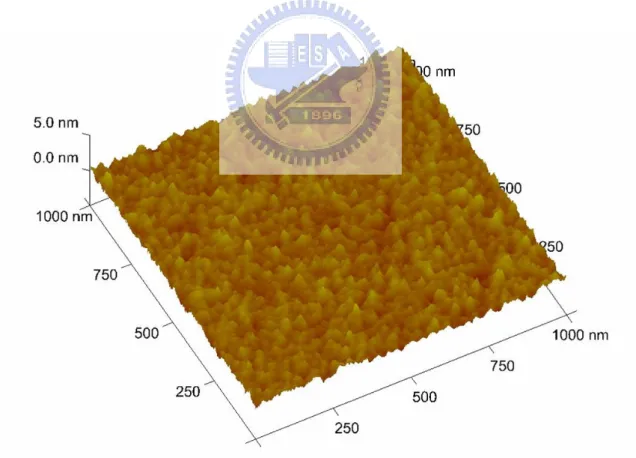
Fig. 2.1 CNT structures of armchair, chiral and zigzag tubules 7 Fig. 2.2 The construction of CNT from a single graphite sheet 7 Fig. 2.3 The relation between properties and structure of CNTs 8 Fig. 2.4 Schematic diagram of arc-discharge system 12 Fig. 2.5 Schematic diagram of laser ablation system 12 Fig. 2.6 Schematic drawings of thermal CVD system 14 Fig. 2.7 Schematic drawing of MPCVD apparatus 16 Fig. 2.8 Schematic drawing of PE-HF-CVD apparatus 16 Fig. 2.9 Schematic drawing of MPCVD apparatus 17 Fig. 2.10 AFM image of AlON buffer layer of 10 nm where shows
rough surface. The rms value of surface roughness is about 1.0 nm
18
Fig. 2.11 Schematic diagram of the growth processes of SWNTs networks assisted by buffer layer
19
Fig. 2.12 TEM images of (a) PtOx thin film and (b) self-assembled Pt
nanoparticles after laser pretreatment
20
Fig. 2.13 Thermo-optical properties of PtOx single layer 20
Fig. 2.14 Schematic diagram of ball-and-stick scooting model 22 Fig. 2.15 TEM image of radiate sea-urchin-like SWNTs 24 Fig. 2.16 Schematic diagram of root growth mechanism -1 24 Fig. 2.17 TEM image of the interface between the multilayered cage
and the single-walled tubes
25
Fig. 2.18 Schematic diagram of root growth mechanism -2 26 Fig. 2.19 Schematic diagram of Yarmulke mechanism 27
Fig. 2.20 Schematic diagram of Solid–liquid–solid growth mechanism 28 Fig. 2.21 Schematic diagram of state change of Raman scattering 31 Fig. 2.22 Raman-active normal mode eigenvectors and frequencies for
a (10,10) nanotube
34
Fig. 2.23 Raman spectra of SWNTs 34 Fig. 2.24 Schematic diagram of Raman vibrational modes of CNTs (a)
G-band mode(b)D-band mode (c)Radial breath mode
35
Fig. 2.25 (a) SWNTs (b) SWNT bundles (c) DWNT (d) MWNT 36 Fig. 2.26 STM image of various chiral angles SWNTs 36 Fig. 2.27 FED display at color mode with red, green, and blue
phosphor column
38
Fig. 2.28 Schematic drawing (a) and physical object (b) of a longitudinal cross section of a CRT fluorescent display with a field emission cathode composed of carbon nanotubes
39
Fig. 2.29 Two probe I-Vbias curve for various values of the gate voltage from a CNTs-based FET
40
Fig. 2.30 Atomic Force Microscopy (AFM) image shows the design of the voltage inverter. (b) Characteristics of the resulting intramolecular voltage inverter
40
Fig. 2.31 SWNT attached to the pyramidal tip of a silicon cantilever for AFM
43
Fig. 2.32 (a)Tapping mode AFM image of a 400-nm-wide, 800-nm-deep trench taken with a bare pyramidal tip. (b) The image taken with a nanotubes attached to the pyramidal tip with the same specimen
44
Fig. 3.1 Flow Chart of the experiment 45 Fig. 3.2 Schematic drawing of MPCVD system 51 Fig. 3.3 Schematic drawing of MPCVD reactor 51 Fig. 3.4 Schematic drawing of scanning local laser heating
pretreatment
Fig. 3.5 Schematic diagram of specimen stacking sequences 55 Fig. 3.6 Schematic diagram of the field emission measurement setup 61 Fig. 4.1 Top-view SEM images of the pretreated catalyst precursor
on silicon wafer without application of buffer layer and with various CoCrPtOx catalyst precursor thicknesses: (a) 10 nm,
(b) 5 nm, (c) 3 nm, (d) 2 nm, (e) 1 nm and (f) 1 nm, respectively, except Fig. 4.1(f) is the catalyst precursor morphology with 10 nm AlON as buffer layer
64
Fig. 4.2 HRTEM micrographs: (a) Top-view and (b) cross-section of pretreated 1 nm catalyst precursor without buffer layer. (c) Cross-section of pretreated 1 nm catalyst precursor with buffer layer. (d) Schematic diagram of Fig. 4.2(c)
66
Fig. 4.3 EDX spectra of the H-plasma pretreated catalyst precursors on Si substrates: (a) 1 nm catalyst precursor without buffer layer and (b) with buffer layer
67
Fig. 4.4 Top-view SEM images of 10-nm-thick (a) oxidized (Ar:O2 =
10:30) and (b) non-oxidized catalyst precursors with H-plasma pretreatment at 515°C for 8 min; and 10-nm-thick (c) oxidized and (d) non-oxidized catalyst precursor with H-plasma pretreatment at 591°C for 10 min. Other conditions: microwave power 600 W, working pressure 30 Torr and H2 100 sccm
6 8
Fig. 4.5 XPS spectra of as-deposited CoCrPtOx film (upper curve) by
PVD and after H-plasma pre-treated CoCrPtOx film (lower
curve)
70
Fig. 4.6 Top view SEM images of after H-plasma pretreated 5-nm-thick (a) Co, (b) CoCrOx and (c) CoCrPtOx films
73
Fig. 4.7 SEM images of the as-grown SWNTs on silicon wafer with different catalyst precursor thickness: (a) 10 nm, (b) 5 nm (c) 3 nm, (d) 2 nm, (e) 1 nm and (f) 1 nm with buffer layer
75
Fig. 4.8 Raman spectra of the as-grown SWNTs film on silicon wafer with different catalyst precursor thickness: (a) 10 nm, (b) 5 nm (c) 3 nm, (d) 2 nm and (e) 1 nm. The RBM peaks and very high intensity ratio of G-band / D-band (43:1) are found
in the (f) 1-nm-thick catalyst precursor with buffer layer Fig. 4.9 HRTEM images of the typical as-grown SWNTs where the
tubes are mainly bundle type and their diameters are ranged from 2~3 nm
76
Fig. 4.10 Typical SEM micrographs of extremely dense and vertically aligned SWNTs film on silicon wafers: (a), (b) tilt-view, (c) is the high magnification image of (b), (d) cross-sectional view, (e) shows very flexible morphology and (f) a fragment of Si substrate, respectively
78
Fig. 4.11 Top-view SEM image of short and entangled SWNTs of sample C
79
Fig. 4.12 (a) Top-view SEM image of re-grown SWNTs with insufficient pretreatment time. (b) Raman spectrum of re-grown SWNTs with suitable pretreatment time
81
Fig. 4.13 Top-view SEM images of catalyst precursor (a)(b) after laser ablation pretreatment and (c) after 10 min. 350 °C H-plasma pretreatment
82
Fig. 4.14 (a) Top-view SEM image and (b) Raman spectrum of low temperature grown SWNTs at 373 °C
83
Fig. 4.15 EDX analysis of as-grown SWNTs removed substrate 86 Fig. 4.16 Field emission current density as a function of electric field
for the SWNTs
87
Fig. 4.17 Thermo-gravimetric properties of a 5-mg as-grown SWNTs. (ramp rate, 10°C/min)
ChapterⅠ
Introduction
1.1 Introduction to single-walled carbon nanotubes
CNTs are one dimension nanostructure of carbon bonded mainly by sp2 bond and crooked by sp3 bonds with hollow and cylindrical construction. We can simply image that it is a graphene sheet [Fig. 1.1(a)] shaped like a roll in nano-scale [Fig. 1.1(b)]. The single-walled CNTs (SWNTs) and multi-walled CNTs (MWNTs) are defined whether the number of the rolled graphene layers is one or more. It is well known that the CNTs have extremely high aspect ratio just because the diameters of CNTs only from 1-2 nm to 8-90 nm, but the length of a tube could be from several nanometers to several micrometers.
(a) (b)
Fig. 1.1 (a) Graphite sheet (b) formed CNT rolled by the graphite sheet
SWNTs have attracted considerable attention in recent years. Various methods have been used for synthesizing SWNTs, e.g. arc discharge [Saito-1995-33], laser ablation[Guo-1995-49] and chemical vapor deposition (CVD)[Lee-2001-245], where the CVD methods are the most effective way to synthesize SWNTs. The SWNTs with random distribution can be easily synthesized. [Delzeit-2001-368] However, the actual growth mechanisms of SWNTs are still a controversy question.
Due to many unique properties of SWNTs, such as high aspect ratio, small radius of curvature, extraordinary mechanical strength and chemical stability, undoubtedly, SWNTs are being developed for many applications like field emission display (FED) [Sander-1998-49], biology technology [Dai-1996-147], fuel cell
[Liu-1999-1127], etc.
1.2 Motivation of this research
SWNTs have recently been considered to be a promising candidate material for use in field emitters, nano-electronic devices (such as single electron transistors) [Collins-2001-706] [Bachtold-2001-1317], and others. In such applications, one of the key issues is to effectively manipulate the nanostructures at lower deposition temperatures in order to be compatible with the IC processes. Recently, low temperature processes to synthesize the catalyst-assisted SWNTs by CVD methods have been widely studied [Qin-1998-3437] [Kurt-2001-1723] [Tsai-2001-NCTU].
However, most of these deposited SWNTs show morphologies in randomly entangled fashions [Delzeit-2001-368]. The methods to grow the well-aligned SWNTs on the desired locations are not quite successful so far.
The treatment of the catalyst to minimize the catalyst particle sizes before CNTs growth represents another technological challenge in SWNTs growth. Physical vapor deposition (PVD) is the most popular approach for depositing catalytic materials, because it is highly compatible with the IC process. The catalyst films are typically treated with H-plasma to become well-distributed nano-particles, and CNT are subsequently grown from these pre-treated catalystic nano-particles. However, the agglomeration of nano-particles is unavoidable during the heating process, which does not particularly favor the fabrication of SWNTs. One way to minimize the catalyst particle size is to use the ultra-thin catalytic film, but the agglomeration effect during H-plasma pretreatment makes it difficultly to form SWNTs[Delzeit-2001-368]. Although Zhong et al. [Zhong-2005-1558] recently reported using Al2O3/Fe/Al2O3 with a sandwich-like
structure to fabricate vertically aligned SWNTs, in which the Al2O3 buffer layer
can inhibit the coarsening of Fe catalyst particles, the presence of the buffer layer on the top or bottom of catalyst layer raises other problems when SWNTs are used in electrical devices, such as adhesion, electrical conductivity and impurities. Accordingly, the purpose of this work was to develop a process to
fabricate the well-aligned SWNTs at low temperatures without buffer layer application. The idea is to use the catalyst precursor (CoCrPtOx) to promote the
miniaturization of nanoparticles and to prevent the agglomeration effect during pretreatment and the initial stage of CNTs growth.
Chapter Ⅱ
Literature review
2.1 Structures and properties of CNTs
Since discovery of CNTs in 1991 [Iijima-1991-56] , many superior properties of CNTs have attracted much attention of the scientists. The excellent properties of CNTs must be closely related to its unique structure. It was proposed that a graphene sheet of (0001) plane can be rolled to become various forms of CNTs structures: armchair, zigzag and chiral CNTs. The CNTs can be pictured as the fullerene-related structures with the end caps containing pentagon and hexagon rings. As shown in Fig.2.1 [Dresselhaus-1996-p756], if a C60 structure is bisected normal
to a five-fold axis, the “armchair” tubule can be formed. ‘Zigzag’ tubule is formed in the way of bisecting C60 structure normal to a three-fold axis. The
other ways of bisecting C60 structure can form the chiral CNTs. The caps of C60,
C70 and C80 [Fig. 2.1(a)] are corresponding to the CNTs structures in armchair,
zigzag and chiral, respectively [Figs. 2.1(c) and 2.1(d)]. In mathematics, scientists proposed a vector to define CNTs [Saito-92-2204]:
Ch = na1+ma2 ≣ (n,m)
(2-1)
while a1 and a2 denoted the unit vectors of graphene sheet. As shown in Fig. 2.2,
the structures of CNTs in zigzag, armchair or chiral form are classified by the θangle or range, i.e. 0o, 30o or 0o<θ<30o, respectively. The chiral vector is expressed as a pair of integers (n, m) for mapping planar graphene sheet. The zigzag, armchair and chiral CNTs are corresponding to the chiral vectors of (n, 0), (n, n) and (n, m), respectively.
In 1992, Hamada and Saito [Hamada-1992-1579] [Saito-1992-2204] proposed theoreticallythat the CNTs can be a conductor or a semiconductor depending on its chirality. Their theories were proved experimentally by Wildoer and Odom
[Wildoer-1998-59] [Odom-1998-62] in 1998, using STM. They indicated that the two
parameters, helicity and diameter, can be adopted to distinguish the metallic from semi-conducting properties of CNTs, i.e. the differences in the band gap and the Fermi energy shift. Among them, the armchair CNTs have two integers n and m equal to each other, thus have bands that cross the Fermi level and therefore are truly metallic. The chiral and zigzag nanotubes had two possibilities: (a) If n-m = 3k, where k is a integer except zero, then it was metallic with an energy gap of about 1.7 - 2.0 eV; (b) If n-m ≠ 3k, then it was semiconducting with an energy gap of about 0.5 - 0.6 eV [Fig. 2.3]. These show the nanotubes electrical properties are very sensitive to the wrapping angle and the tube diameter.Ballistic transport in the CNT channel was assumed.
Fig. 2.1CNT structures of armchair, chiral and zigzag tubules.[Dresselhaus-1996-p756]
Fig. 2.3 The relation between properties and structure of CNTs[Saito-1992-2204]
In addition to the special features on electrical properties of CNTs, another key point of what scientists concerned is their field emission properties. The field emission is an electron emission phenomenon through tunneling effect when an electric field is applied on the surface of a material with negative potential. Due to suitable geometric contours, high thermal stability, good mechanical strength and high chemical stability, CNTs becomes a good field emission material. The field emission is much more fascinating than thermal emission since it just needs to apply a low electrical field (~V/μm) at room temperature. Usually, the field emission properties can be expressed by Fowler-Nordheim equation [Spindt-1976-5248]:
(2-2) (2-3) (2-4) with A=1.54×10⁻⁶ ,B=6.87×10⁷ (2-5)
where I , V , φ, α and β are the field emission current (A), an applied
voltage (V), a work function of material (eV), the effective emission area (m2), and the field enhancement factor, respectively. Base on Eq. 2-2, one can obtain:
(2-6)
The ln( 12)
V versus V
1 curve is called F-N plot. A material with good field
emission properties often shows a negative slope on the F-N plot. Base on Eq. (2-2), the ways to improve the field emission properties of a material can be achieved by increasing the effective emission area, α, and the field emission factor, β, which is related to the aspect ratio or geometric factor of emitter. Furthermore, the too-close distance between emitters can deteriorate their emission properties, which is often called the screen-effect. [Gröning-2000-665] This
signifies that the manipulation of the tube number density is also an important issue in field emission studies.
(
)
⎥ ⎥ ⎦ ⎤ ⎢ ⎢ ⎣ ⎡ × = − 2 1 7 2 1.44 10 exp 1 . 1 φ φ β αA B a ⎟ ⎠ ⎞ ⎜ ⎝ ⎛ − = V b aV I 2exp β φ32 95 . 0 B b= ⎟ ⎠ ⎞ ⎜ ⎝ ⎛ − = ⎟ ⎠ ⎞ ⎜ ⎝ ⎛ V b a V I 1 ln ln 2In addition to special marvelous electrical properties, the mechanical properties, e.g. the reported Young’s modules may reach over 1 TPa [Eric-1997-1971] which makes CNTs the stiffest material in the world. CNTs also behave elongation to failure of 20-30% [Pan-1999-3152] with a high tensile strength about 60 GPa[Yu-2000-637]. These experiment values enable the CNTs to become the highest strength/weight ratio material on earth, and to be used for potential applications in reinforcement of the composites.
Furthermore, thermal manage is now a very hot research in the world and the thermal conduction of CNTs are also excellent. Che et al. [Che-2000-65] evaluated thermal conductivity of 10-nm-long CNTs are great than 2800 W/mK, almost equal to diamond. Berber et al. [Berber-2000-4613] predicted the thermal conductivity of (10,10) SWNT is about 6600 W/mK at room temperature. This is a very important support for their electronic and thermal applications.
2.2 Synthetic methods of SWNTs
There are many methods being developed to synthesize SWNTs, where arc-discharge, laser ablation and chemical vapor deposition (CVD) are the most popular methods [Lee-2001-245]. In those methods, carbon sources can be in gas or solid phases. The morphology and properties of SWNTs are often controlled by manipulating the following process parameters: substrate temperature, precursor
gases and gas ratio, catalyst, pretreatment conditions, applied bias, etc. However, the proposed methods still suffer the following problems: low yielding, low uniformities in structure and property, etc.
(a) Arc-discharge method[Saito-1995-33]
Arc-discharge method is believed to be the earliest way to synthesize CNTs. When CNTs were first identified by Iijima[Iijima-1991-56], it was produced by this method. Figure 2.4 shows the schematic diagram of the arc-discharge system
[Saito-1995-33]. There are two graphitic rods as anode and cathode. Between these
two electrodes, arcing occurs when DC voltage is applied. In the situation of anode containing small amount of catalyst such as Fe, Co, Ni and Y, the SWNTs can be synthesized[Bethune-1993-605], and MWNTs can be fabricated by using pure graphite as two electrodes. Generally, the discharge is operated at a voltage range between 20 and 40 V with current from 40 to 100 A under He or Ar atmosphere of 10-500 Torr. Carbon clusters collided out from the anodic graphite rod by electron bombardment are deposited on the cathode surface. The production on cathode may include amorphous carbon, fullerenes, carbon cluster, carbon nanotubes and varieties of other carbon structures. Therefore, purification of the nanostructures is generally an important issue for applications. Another drawback of this process is its low yielding in producing CNTs.
Fig. 2.4 Schematic diagram of arc-discharge system [Saito-1995-33]
(b) Laser ablation[Guo-1995-49]
Laser ablation method was first reported by Guo’s group in 1995[Guo-1995-49], as shown schematically in Fig. 2.5. There is an incident laser beam for vaporizing graphite target under helium or argon gas atmosphere at pressure of 500 Torr. The productions are swept out by the flowing gas and to be deposited on the water cooled collector. Therefore, it is also called laser vaporization method. The graphite target containing Co, Ni, Fe, or Y is a more favor condition to form SWNTs.
(C) Chemical vapor deposition (CVD)
The CVD method is a mature technique in thin film processes. Most of films can be fabricated by CVD method, including metals, semiconductors and insulators. It is essential for CVD process to introduce some forms of the energy to decompose precursor gases and deposit the reaction product on the substrate surface. The introduced energy may include thermal, microwave, RF, or others. Thus, it gives rise to different process names, depending on the source of the applied energy.
(1) Thermal chemical vapor deposition: [Lee-2001-245]
Figure 2.6 shows a schematic diagram of thermal CVD apparatus in the synthesis of carbon nanotubes. The method was used pyrolysis of hydrocarbon source to synthesize the SWNTs. This method is also catalyst assisted SWNTs growth method and the quality of SWNTs is sensitive to the pyrolysis temperature. The specimen is placed in a quartz boat with coated transition metals or theirs alloy on a substrate, and then the boat is positioned in a CVD reaction furnace, and nano-size fine catalytic metal particles are formed after an additional etching of the catalytic metal film with NH3 gas at a temperature in
750 to 1050°C. Reaction gas is supplied in one end of the apparatus, and gas outlet in the other. The merit of this method is easily to deposit large area, uniform and good quality of SWNTs. However the drawback is not compatible
with IC (integrated circuit) process due to working temperature over 600°C.
Fig. 2.6 Schematic drawings of thermal CVD system [Lee-2001-245]
(2) Plasma enhanced CVD (PECVD): [Qin-1998-3437]
PECVD system was employed to deposit the SWNTs with many merits comparing with other methods, e.g. compatible process with IC process, cheaper, less contamination, high yielding and controlled alignment of SWNTs, thus current attention has focused on developing new techniques for the preparation of vertically aligned SWNTs by using CVD methods.
According to the methods of plasma excitation can be classified the different plasma system such as microwave plasma CVD (MPCVD), RF or DC bias excited plasma CVD (PECVD), microwave plasma assisted hot filament CVD (MP-HFCVD) and electron cyclotron resonance CVD (ECR-CVD) and so
fourth. Generally, the power supplies for discharge of plasma CVD are DC bias; radio frequency (RF) (13.56 MHz) and microwave (2.47 GHz) are typical of high frequency power supply. Using the plasma CVD process to produce SWNTs can be prepared by applying decomposition of hydrocarbon (such as CH4, C2H2, C2H4 and C6H6) or monoxide and even decomposed of metal
complex on various substrates that coated transition-metal film.
The common used of microwave plasma CVD, such as MP-CVD, PE-HF-CVD, and ECR-CVD, to synthesize SWNTs can be ranked in terms of their working pressure, where MP-CVD or PE-HF-CVD and ECR-CVD were operated with the pressure range of P < 10-3 Torr and 10-1 < P < 100 Torr, respectively. The MP-CVD system [Qin-1998-3437] as shown in Fig. 2.7, with the high density of plasma ball permits a contamination-free and a modification of plasma shape through tuning of the cavity. The PE-HF-CVD system applied the current on the tungsten filament to efficiently increase temperature in the chamber [Kurt-2001-1723] as shown in Fig. 2.8 The ECR-CVD as shown in Fig. 2.9 is known for its own advantages of high dissociation percentage of the precursor gas, high uniformity of plasma energy distribution and large area of CNTs deposition [Tsai-2001-NCTU].
Fig. 2.7 Schematic drawing of MPCVD apparatus [Qin-1998-3437]
Fig. 2.9 Schematic drawing of MPCVD apparatus [Tsai-2001-NCTU]
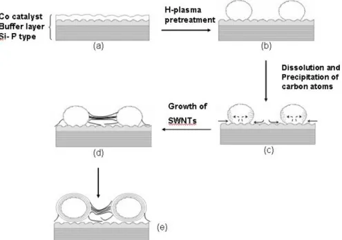
(d) Buffer layer-assisted growth of SWNTs
Buffer materials are most effectively to promote SWNTs formation. Wang et al. [Wang-2006-in press] demonstrate that AlON buffer layer is the best material for SWNTs fabrication. Moreover, the results also indicate that the favorable conditions for synthesizing SWNTs networks are a high substrate temperature, low CH4/H2 ratio and thin catalyst thickness with AlON as the buffer layer
material. The roughness of AlON film is presenting a rough (~1 nm) surface [Fig. 2.10], whereas Si wafer surface is quite neat. These results suggest the protrusion on rough buffer layer (e.g., AlON) can cause instabilities on Co
Plasma 2.45 GHz Microwave Heater DC Bias Pump Gas Inlet Quartz dome Magnetic coil Sample
catalyst surface and form nuclei sites for tubes growth afterwards. They also have measured the roughness of other buffer materials, such as AlN, TiN, and TiO2. The results show their surface are quite smooth and roughness (Rrms) are
on the order of angstroms at most, show hardly effect to enhance SWNTs. Figure 2.11 shows the growth processes of buffer layer assisted growth of network SWNTs.
Fig. 2.10 AFM image of AlON buffer layer of 10 nm where shows rough surface. The rms value of surface roughness is about 1.0 nm. [Wang-2006-in press]
Fig. 2.11 Schematic diagram of the growth processes of SWNTs networks assisted by buffer layer. [Wang-2006-in press]
(e) Alloy catalyst-assisted growth of SWNTs
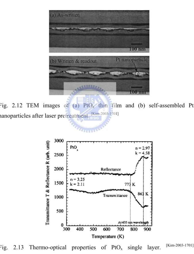
Alloy catalysts were recently employed to growth CNTs like CoMo, FeNi, CoPt, FePt [Kuo-2003-799] and so on. But no extremely dense vertically aligned SWNTs were grown by alloy catalysts in the past. PtOx has been recentlyused in
optical storage media and nonvolatile memory technology because of its explosive effect of the decomposition of PtOx at an appropriate process
temperature. Kim et al. [Kim-2003-1701] proposed that PtOx film will decompose to
Pt nano-particles and O2 by laser thermal pretreatment. The decomposition
temperature is approximately 500°C (1 atmosphere in air). Figures 2-12(a) and 2-12(b) show that PtOx film was self-assembled to nano-particles by laser
the decomposition of PtOx film to Pt nano-particles and O2 [Fig. 2.13]. Thus, it
is so interesting to adopt PtOx with other metals, like Co and Cr, to be
alloy-catalyst for synthesis of SWNTs.
Fig. 2.12 TEM images of (a) PtOx thin film and (b) self-assembled Pt
nanoparticles after laser pretreatment. [Kim-2003-1701]
Fig. 2.13 Thermo-optical properties of PtOx single layer. [Kim-2003-1701]
2.3 Growth mechanisms of SWNTs
Regarding the use of CVD methods for SWNTs growth, many growth mechanisms have been proposed[]. However, most of the mechanisms are based on the original model of carbon nanofibres proposed in 1970s by Backer.
[Backer-1978-14] It is believed that nanotubes grow as carbon precipitates from a
supersaturated metal catalyst that resides at either the base or the tip of a growing nanotube. Catalyst/substrate interactions and temperature gradients across the catalyst particle are considered to be important factors that determine the growth mechanism. Catalyst size was believed to determine the CNT diameter, and SWNT was synthesized when catalyst size is about 1~2 nm. However, most of these models were proposed without sufficient and systematic supporting experimental evidence, and they often lacked details about the physical mechanisms and the effects of various process parameters. Thus, the kinetics of nanotube nucleation and growth are not well known yet. Other growth mechanisms are described as follows:
(a) Ball-and-stick catalyst scooting model [kuo-2004-p.9-10]
Birkett et al. [Birkett-1997-111] proposed that transition metals show a high propensity for decoration fullerene surfaces. A carbon fragments bind to the metal clad fullerene and they may self-assemble as a surrounding circular hexagonal chicken-wire-like fence. Once formed as a belt, the network could
propagate as a cylinder, so called open edge growth. This model predicts the SWNT diameter will be d(C60) + 2*d(Interplanar distance), i.e. 0.7 nm + 2(0.34)
nm = 1.38 nm ,which is in excellent agreement with observation. Another possible model was scooter mechanism[Thess-1996-483] which considered that a few metal atoms chemisorbed and scooted around the open edge of the sheet and kept tube open and grow. When metal atoms aggregated and lost its kinetic energy for scooting, SWNT growth will stop. Figure 2.14 shows the schematic diagram of ball-and-stick scooting model.
Fig. 2.14 Schematic diagram of ball-and-stick scooting model [Birkett-1997-111]
(b) Root growth mechanism
diameter are much smaller than catalyst, this is called root growth mechanism. Saito et al.[saito-1994-L526] proposed that when catalyst metal is evaporated together with carbon by arc discharge, carbon-metal alloy particles are formed on the cathode surface. Since the carbon-metal compound soot was produced in a carbon-rich at atmosphere, the initial alloy particles in a liquid phase contained more carbon than solubility limit in a solid state. Therefore, with the decrease of temperature of the cathode, the liquid alloy particles begin to segregate excess carbon on their surfaces. When the cooling of particles proceeded at a moderate rate and the supersaturation of carbon in metal particles was not so high, the carbon gradually segregated on the surface and formed graphitic layers one by one. When cooling was rapid and the initial content of carbon in a particle was high compared with that in the process mentioned above, the supersaturation of carbon became rather high. According to the classical nucleation theory, high supersaturation would bring about nucleation of graphite at numerous sites on the surface of a particle. Since the formation of flakes of graphitic occurs suddenly, a large number of tiny graphitic flakes are formed. These flakes curl and then close their open ends in order to saturate dangling bonds at their periphery. Among this random assembly of graphitic flakes, seeds of SWNTs may be formed [Figs. 2.15 and 2.16].
Fig. 2.15 TEM image of radiate sea-urchin-like SWNTs [saito-1994-L526]
Fig. 2.16 Schematic diagram of root growth mechanism -1 [saito-1994-L526] Zhou et al.[zhou-1994-1593] proposed another model that SWNTs was separated from catalyst surface by graphite layers, as shown in Fig. 2.17. Furthermore,
Gavillet et al[Gavillet-2001-275504] suggest a common growth mechanism based on a vapor-liquid-solid model. The first step of the process is the formation of a liquid nanoparticle of metal supersaturated with carbon [Fig. 2.18(a)]. And then there is a competition between the formation of a graphitic sheet [Fig. 2.18(b)] and the nucleation of single-wall nanotubes [Fig. 2.18(c)]. In order to obtain long nanotubes [Fig. 2.18(d)], the root-growth process should continue for a sufficiently long time, until local temperatures are too low, leading to the solidification of the nanoparticles. Figures 2.18(e) and 2.18(f) show that nucleation did occur but growth did not take place so that carbon has partly condensed into amorphous carbon flakes or into a few graphitic layers.
Fig. 2.17 TEM image of the interface between the multilayered cage and the single-walled tubes [zhou-1994-1593]
Fig. 2.18 Schematic diagram of root growth mechanism -2 [Gavillet-2001-275504]
(c) Yarmulke mechanism
This model was proposed by Dai et al.[Dai-1996-471] that SWNTs are formed on molybdenum nanoparticles in the size range of 1~4 nm by the disproportionation of CO at 1200°C, indicates that there can be a slight variation in the size. And they observed that SWNTs were close end and the catalysts were on the top of tubes. So yarmulke mechanism was supposed that carbon atoms were chemisorbed on the catalyst to form yarmulke firstly. And then carbon source decomposed and diffused into catalyst, so that SWNTs grew longer. In the case of organometallic precursors, it seems that SWNTs of ~1 nm diameter are produced under controlled conditions. When the organometallic concentration is high, MWNTs are formed around the catalyst particles with sizes in the range of 5~20 nm. In the larger size range, >50 nm, graphite-covered metal particles are predominantly formed [Fig. 2.19].
Fig. 2.19 Schematic diagram of Yarmulke mechanism [Dai-1996-471]
(d) Solid–liquid–solid growth mechanism
Gorbunov et al.[Gorbunov-2002-113] proposed that a molten catalyst nanoparticle penetrates an amorphous carbon aggregate dissolving it and precipitating carbon atom [Fig. 2.20(a)]. These atoms arrange in a graphene sheet [Fig. 2.20(b)], whose orientation parallel to the supersaturated metal-carbon melt is not
energetically favorable. Any local defect of this graphene sheet will result in its buckling [Fig. 2.20(c)] and formation of a SWNT nucleus [Fig. 2.20(d)]. Further precipitating carbons incorporate in edges of growing nanotube [Fig. 2.20(e)] which are anchored to the catalyst nanoparticle by overlapping its unsaturated sp2 orbitals with the metal orbitals of the catalyst nanoparticles.
Fig. 2.20 Schematic diagram of Solid–liquid–solid growth mechanism
[Gorbunov-2002-113]
2.4 Process parameters of SWNTs growth in MP-CVD
morphology, growth mechanism, tube number density, structure, etc. (a)Catalyst:
Different catalysts own distinct properties and the growth of SWNTs can be affected. If a catalyst particle is tightly sintered, it becomes harder to melt during reduction or pretreatment process. In other words, to form nano-scaled liquid droplets which provides the embryo of SWNTs is more difficult, so the same catalyst leads to the growth of nano-sheet instead of nanotube with lower growth temperature.[Lin-2002-922] The ways of depositing catalyst also cause influences as well.
(b)Growth temperature:
Besides the above-mentioned influence of catalyst reduction, temperature can also affect the diffusion rate of carbon atoms inside the catalyst. With higher growth temperature, the diffusion rate within catalyst becomes quickly and direct affects the growth rate, length and tube number density of CNTs. Also, the precursor gases decompose amount can be different with different temperature. It changes the mixing concentrations of precursors. In addition, the crystalline of graphene layer becomes better with higher growth temperature.
(c)Gas
This condition includes precursor type, flow rate and gas ratio. In literature, many carbon source and reducing gas has been used. [Yun-2003-6789] [Lin-2002-922] Different gas types have distinct pyrolysis temperature and different
bombardment effect in plasma environment. (d)Working pressure:
When the inlet and pumped out gas flow reach a steady state, the pressure in chamber is called working pressure. The main effects of this parameter are the plasma behavior. With higher pressure, the mean free path of radical decrease but collision probability increase. The plasma induced self-bias will change with different pressure.
(e)Growth time:
Growth time usually changes the length of SWNTs. But after catalyst is poisoned, the growth time won’t affect it any more.
2.5 Analyses of SWNTs
(a) Raman spectroscopy analysis
(1)Measurement principle[Rao-1997-187]
Raman spectroscopy provides information about molecular vibrations that can be used for sample identification and quantitation. The Raman effect arises when a monochromatic light (laser) shines on a sample and excites molecules in the sample, which subsequently scatter the light. While most of this scattered light is at the same wavelength as the monochromatic light, some (±0.0001%) is scattered at a different wavelength. This in elastically scattered light is called
Raman scatter. It results from the molecule changing its molecular motions. The energy difference between the monochromatic light and the Raman scattered light is equal to the energy involved in changing the molecule’s vibrational state. This energy involved in changing the molecule’s vibrational state. This energy difference is called the Raman shift. Several different Raman shifted signals will often be observed; each being associated with different vibrational or rotational motions of molecules in the sample. Figure 2.21 shows the schematic diagram of state change of Raman scattering.
(2)Raman shifts of SWNT[Raravikar-2002-235424]
SWNT has 15 or 16 Raman-active modes, but some of their Raman scattering are difficult to detect, so only 7 Raman-active modes can be observed in measurement, as shown in Fig. 2.22.
Figures 2.23(a) and 2.23(b) show a typical Raman spectrum of SWNT sample taken at room temperature. The two prominent peaks with a peak position of 182 and 264 cm-1 in Fig. 2.23(a) are the two RBM (radial breath mode,A1g) peaks. The two peaks from Fig. 2.23(b) at peak positions ~1590 and
~1350 cm-1 belong to the G-band (tangential stretching mode,E2g) and D-band
( from amorphous carbon,A1g), respectively.
Figures 2.24(a), 2.24(b) and 2.24(c) show the G-band, D-band vibrational modes and the RBM’s in SWNTs respectively. In graphite and CNTs, the G-band Raman vibrational modes are present due to the in-plane vibrational movement of carbon atoms, which involves a combination of stretching and bending of the carbon-carbon (C-C) bonds. The disorder-induced D-band Raman vibrational mode, which is a highly dispersive spectral feature, is also present in these materials due to the collective in-plane vibrational movement of atoms towards and away from the center of the hexagons formed by the covalently (sp2) bonded carbon atoms. Therefore, the D-band mode involves stretching and bending of C-C bonds.
The RBM is a unique feature in the Raman spectrum of SWNTs and involves a collective vibrational movement of the carbon atoms towards and away from the central axis of a SWNT. The RBM oscillations are associated with a periodicity imposed on a graphene sheet by wrapping it into a finite-size (small diameter) tube. Consequently, the associated RBM Wavelength and frequency are directly related to the perimeter of the nanotube. Base on this relationship, as the diameter of the nanotube increases, the RBM frequency shifts to lower wave numbers. For larger and, particularly, MWNTs, the RBM frequency becomes very small and, at the same time, the intensity of the radial breathing mode decreases and ultimately becomes undetectable by Raman spectroscopy measurements. Hence Dresselhaus et al. [Dresselhaus-2002-2043]proposed that the frequency of the RBM are:
ω = ä(cm-1 nm)/d(nm) (2-7)
where ä for the Si /SiO substrate is experimentally found to be 248 cm-1nm for isolated SWNTs, ω is the peak position, d is the SWNT diameter and RBM is independent of chiral angle. Furthermore, Tuinstra et al. [Tuinstra-1970-1126] proposed that the Raman spectra of single crystals of graphite shows only one mode at 1575cm-1 and as the increase of defects and disorder, D-band will show, so the IG/ID ratio can be used to determine the graphitized degree of SWNTs.
Fig. 2.22 Raman-active normal mode eigenvectors and frequencies for a (10,10) nanotube [Rao-1997-187]
Fig. 2.24 Schematic diagram of Raman vibrational modes of CNTs (a) G-band mode (b)D-band mode (c)Radial breath mode [Raravikar-2002-235424]
(b) High-resolution transmission electron microscope (HRTEM) [Flahaut-2000-249] HRTEM is the most direct method to analyze the structure of SWNT, however it is not easy to obtain a clear image of one SWNT. The main reasons are the structure of SWNT will be destroyed easily by high energy electron beam and electron scattering are not apparent because of SWNT is composed of so few carbon atoms. Furthermore, SWNT is hard to be built on stilts to avoid the background interference from copper grid and SWNTs dispersion are also an important problem. Figure 2.25 shows the HRTEM images of (a) SWNTs (b) SWNT bundles (c) DWNT (d) MWNT.
Fig. 2.25 (a) SWNTs (b) SWNT bundles (c) DWNT (d) MWNT [Flahaut-2000-249]
(c) Scanning tunneling microscope (STM)
STM can directly observe surface carbon atoms of SWNTs, providing information of carbon atoms site and arrangement. So we can measure length and chiral of SWNTs, as shown in Fig. 2.26.
2.6
Applications of SWNTs
Many researchers and engineers have been devoted to combine the CNTs with living. There are a lot of possible applications of CNTs products such as FED, field effect transistor (FET), hydrogen storage, etc. Until now, lots of prototypes of these applications have been published. Thus, it is believed that more and more commercial products will be published soon in the feature. (a) Electron field emission elements:
The electron field emission elements, as implied by the name, utilized the field emission properties of CNTs. Among all of them, the closest to our life is FED. It is a next generation display after plasma display panel (PDP) and liquid crystal display (LCD) technologies. The theorem of formation of image is to use CNTs as cathode, then applies the potential between cathode and anode. Electrons emits from cathode to anode with phosphors which generate illumination. Ultra thin, wider view angle, superior brightness and low operation power are main advantages of FED. Samsung corporation had been public the
4.5” FED prototype in 1999 [Fig. 2.27].[Choi-1999-3129] And the electron source like SEM filament[Chow-1992-1] or X-ray tube[Yue-2002-355] can also employ the CNTs as electron emitters, which possess longer life, small energy spreading and power-saving significantly. Another field emission application related to general public is cathode-ray tube (CRT) lighting elements. The original has been published in 1998 by Ise Electronics corporation, Japan.[Saito-1998-L346] The fabricated CRTs are of a triode type, consisting of a cathode (nanotubes field emitter arrays), a grid and an anode (phosphor screen) [Figs. 2.28(a) and 2.28(b)]. The maxima brightness with anode at 200μA is 64000 cd/cm2. Stable electron emission, adequate luminance and long life (over 10000 hours) are demonstrated. It can be applied to a giant outdoor display or ultra-high quality color CRT displays.
Fig. 2.27 FED display at color mode with red, green, and blue phosphor column.
(a) (b)
Fig. 2.28 Schematic drawing (a) and physical object (b) of a longitudinal cross section of a CRT fluorescent display with a field emission cathode composed of carbon nanotubes. [Saito-1998-L346]
(b)FET
FET is a very important electronic device in history. The overwhelming majority of FET is silicon or Ⅲ-Ⅴ based just because these materials are semiconductors. But some of CNTs also have semiconducting properties, it makes researchers want to fabricate the CNTs based FET. In 1998, Sander reported the room-temperature transistor based on a single SWNTs FET.
[Sander-1998-49] Fig. 2.29 shows the I-V curve of the CNT-FET. In 2001, Derycke in
IBM corporation prepared both p-type and n-type nanotubes transistors to build the first nanotubes-based logic gates: voltage inverters [Figs. 2.30(a) and
2.30(b)].[Derycke-2001-453] Surely, it still have lots of complicated problems to mass production above-mention devices, but these results have told that the nano-electronics is not hollow words any more.
Fig. 2.29 Two probe I-Vbias curve for various values of the gate voltage from a
CNTs-based FET. [Sander-1998-49]
(a) (b)
Fig. 2.30 (a) Atomic Force Microscopy (AFM) image shows the design of the voltage inverter. (b) Characteristics of the resulting intra-molecular voltage inverter. [Derycke-2001-453]
(c) Lithium intercalation
The basic principle of rechargeable lithium batteries is electrochemical
intercalation and de-intercalation of Li in both electrodes. An ideal battery has a high-energy capacity, fast charging time and long cycle time. The capacity is determined by the Li saturation concentration of the electrode material. The SWNTs have shown to possess both high reversible and irreversible capacities
[Gao-1999-153].
(d) Hydrogen storage material
Face to possible energy-crisis of gasoline, people has started to find the substitution methods for many years. Fuel cell was considered to have potential among all of solutions. Once it does be generated, its use as a fuel that creates neither air pollution nor greenhouse gas emissions. But it needs a huge hydrogen storage capability material. SWNTs just can play this role.SWNTs can absorb higher hydrogen than conventional materials. A H2 uptake of 4.2 weight %,
which corresponds to a H/C atom ratio of 0.52, was obtained by these SWNTs with an estimated purity of 50 weight %. Also, ~80% of the adsorbed H2 can be
released at room temperature. These results indicate that SWNTs are highly promising for H2 adsorption even at room temperature [Liu-1999-1127]. The hydrogen
storage mechanisms of CNTs are still not well known yet, and these properties usually occur at high pressure or low temperature environment. It remains
impossible to apply on commercial product so far. (e) Composite materials
The SWNTs may be used as reinforcements in high strength, Low weight, and high performance composites due to their excellent mechanical properties. A main advantage of using SWNTs for structural polymer composites is that SWNT reinforcements will increase the toughness of the composites by absorbing energy during their highly flexible elastic behavior. Other advantages are the low density of the nanotubes, an increased electrical conduction and better performance during compressive load, or induced high thermal conductivity reinforced material.
(f) Otherapplications
Atomic Force Microscope (AFM) is employed to obtain the surface morphologies and roughness. It uses a probe scanning the surface of sample, and an incident laser beam irradiates the arm of probe reflecting to a detector which passes signals to computer and draws the images. In order to obtain a high resolution images, the tip must be ultra thin, extremely sharp and high strength. General type of AFM tip is made of Si3N4. The first article that utilized SWNTs
as AFM tip was reportedin 1996[Fig. 2.31]. [Dai-1996-147] From Fig. 2.32, one can clearly see the SWNTs tip shows the better image resolution. At the same time, SWNTs with excellent mechanical properties can make the damage ratio of tip
decrease as low as possible. It has been some commercial products of SWNTs AFM tip at present.
In 1998, Wong demonstrated that CNTs tip can be used for chemical and biological discrimination.[Wong-1998-52] Another possible application applied to biotechnology of medicine carriers are developing as well. In the feature, people will easily get to know what disease that we get. Also, people can use CNTs filled with drags injecting into body, then induce it to the proper position relaxing the medicine to destroy the etiology without hurting normal cell nearby.
Fig. 2.31 SWNT attached to the pyramidal tip of a silicon cantilever for AFM.
(a) (b)
Fig. 2.32 (a)Tapping mode AFM image of a 400-nm-wide, 800-nm-deep trench taken with a bare pyramidal tip. (b) The image taken with a nanotubes attached to the pyramidal tip with the same specimen.[Dai-1996-147]
Chapter III
Experimental Methods
3.1 Flow chart
Fig. 3.1 Flow Chart of the experiment
p-type Si (100) substrate
Catalyst precusor coating by PVD (CoCrPtOx, CoCrOx, Co)
H-plasma pretreatment by MPCVD SWNTs deposition by MPCVD FE-SEM TEM Raman TEM FE-SEM TGA
AlON buffer layer coating by PVD
Field emission
XPS EDX
Scanning local laser heating pretreatment
Figure 3.1 shows the experimental flowchart for the fabrication and analyses of the catalyst precursor-assisted SWNTs. First, the CoCrPtOx films to
act as catalyst precursor were deposited by physical vapor deposition (PVD) and buffer layers were prepared by DC reactive sputter. Then, two type of pretreatment were used. (1) H-plasma pretreatment was performed in microwave plasma chemical vapor deposition (MP-CVD) system to carry out reduction of oxidized CoCrPtOx film on silicon wafer. The specimens were subsequently
heated up to grow SWNTs in an appropriate CH4/H2 atmospheres for several
minutes at appropriate chamber pressure. (2) Local laser heating pretreatment was operated using 659 nm pump laser to heat numerous spots on substrate surface up to ~700 oC, and then transferred specimens to MPCVD chamber to synthesize SWNTs on Si substrate. The morphologies of the pretreated catalyst precursor were studied by scanning electron microscopy (SEM). The size and distribution conditions of catalyst particles after pretreatment on the silicon wafer were characterized from grinding cross-section and plane view samples by transition electron microscopy (TEM). Additionally, X-ray photoelectron spectroscopy (XPS) was employed to characterize binding energy of CoCrPtOx
layer at as-deposited and after H-plasma pretreatment to analyze the self-assembly mechanism. The morphologies, microstructures and bonding structures of the as-grown SWNTs were investigated by SEM, TEM and Raman
spectroscopy with a 632.8 nm He-Ne laser, etc. The field emission measurements (J-E) of the specimens were conducted by the simple diode configuration and performed in high vacuum. The oxidation resistance properties of as-grown SWNTs was measured by thermal gravimetric analysis (TGA).
3.2 Raw materials (a) Substrates:
Silicon wafer [P-type (100)] (b) Source gases:
Hydrogen gas (purity 99.9995%) Jian Ren Chemical Co. Methane gas (purity 99.999%) San Fu Chemical Co. Oxygen gas (purity 99.9995%) Jian Ren Chemical Co.
Nitrogen gas (purity 99.998%) Jian Ren Chemical Co. Argon gas (purity 99.9995%) San Fu Chemical Co. (c) Target:
CoCrPt Co 57.08 %, Cr 10.97 %, Pt 31.95 % CoCr Co 67.19%, Cr 32.81%
3.3 Strategy of self-assembly CoCrPtOx catalyst precursor
As shown in Fig. 2.12, the oxidized phase of PtOx is unstable and can be
easily reduced back to metallic state with very fine size when temperature is approximately 500 °C [Kim-2003-1701]. Hence, it has been recently used in optical storage media and nonvolatile memory, as shown in section 2.2. Additionally, Co is the good element for carbon species dissolubility and Cr2O3 are revealed to
suppress the grain growth of Ni-Cr alloy effectively [Shaijmon-2005-192]. Combining these unique properties, oxidized film of CoCrPt deposited by PVD is acted as the catalyst precursor to fabricate vertically well-aligned SWNTs and synthesize SWNTs with low process temperature on Si substrate in this study.
3.4 Catalyst precursor and buffer layer deposition procedures (a) Catalyst precursor
The CoCrPtOx thin films which were as catalysts were coated on a
(100)-oriented p-silicon wafer with and without buffer layer using a pure CoCrPt target by PVD (Helix 6-gun) in a mixed argon and oxygen atmosphere. The argon and oxygen ratio for depositing was 10:30 (sccm/sccm) and the deposited thickness of CoCrPtOx films were 1, 2, 3, 5, 10 nm.
(b) Buffer layer
was used in this study. AlON film was deposited on a (100)-oriented p-silicon wafer by DC reactive sputtering (Unaxis Cube Trio) using an Al target in a gas mixture of oxygen, nitrogen and argon. The deposited thickness of AlON film was 10 nm which was the best thickness to assist catalyst particles in distributing, as shown in section 2.2[Wang-2005-1906].
3.5 Microwave plasma chemical vapor deposition system (MPCVD)
The schematic diagram of MPCVD system is shown in Fig. 3.2. The main components of the system can be divided into six parts: the microwave generator, wave guides, reaction chamber, gas flow controller, gas pressure controller and pumping system. The microwave generator of microwave source system (Frequency 2.45 GHz, Power 1.3 kW) was produced by Tokyo electronic Corp. Ltd. The reaction chamber contains quartz tube (inner: 47 mm, outer: 50 mm, China Quartz Corp. Ltd), stainless chamber, stainless holder and rotary pump (Hitachi Corp. Ltd). As Fig. 3.3 shown, sample holder is manufactured by stainless steel, it can bear high working temperature and reduce vacuum pollutions while plasma working. The upper electrode that was made by stainless steel is connected to the DC power supply output. The upper electrode (ground) and substrate holder (negative) were employed to applying the substrate negative bias. The substrate temperature is measured by thermal couple
which equipped in the holder. Mass flow control (MKS model 247) system is used to regulate the flow rate of reacting gas while depositing. Besides, the flow rate controller with different range (1-10 sccm, 10-100 sccm) of flow rate of mass flow control system can be properly adjusted for different gas (Ar, NH3, H2,
CH4, C2H2). The low pressure (0.1~100 Torr) of chamber can be detected by
thermal couple of vacuum gauge and absolute pressure gauge (MKS Baratron). The work pressure of chamber can be regulated stably by throttling valve. The degree of the throttling valve was controlled by APC controller (MKS model 263). There is no external heater system equipped on MPCVD. The plasma is used to heat the substrate as the heat source. Cooling cycle system is made up of the refrigerator with closed cooling water and the conduit.
Fig. 3.2 Schematic drawing of MPCVD system
3.6 Pretreatment methods
3.6.1 H-plasma pretreatment by MPCVD
After catalyst precursor and buffer layer deposition, the specimen was transferred in air to the chamber of MPCVD which was pumped down to its base pressure. Hydrogen plasma was utilized to activate the CoCrPtOx film and
change surface morphology of it. The purpose of this part is to find out the optimum conditions of H-plasma pretreatment to obtain the small average size distribution and appropriate density of catalyst nano-particles. The most optimum CoCrPtOx catalyst precursor pretreatment conditions were: microwave
power 600 W, working pressure 30 Torr, sample temperature 580 oC, H2 flow
100 sccm and process time 10 minutes. Finally, we draw three straight lines on SEM micrograph and calculate the average particle size by the ratio of line length to particle numbers.
3.6.2 Scanning local laser heating pretreatment
For scanning local laser heating pretreatment, catalyst precursor-deposited sample was transferred to the chamber of two laser static tester (Tueopicts, 633-nm-wavelength cw model diode laser and 659-nm-wavelenth duration mode diode laser). The 633-nm laser was used to monitor the reflectivity change to focus another 659-nm laser. Then using 659-nm pump-laser to heat numerous spots on substrate surface simultaneously to carry out reduction of oxidized
![Fig. 2.1 CNT structures of armchair, chiral and zigzag tubules. [Dresselhaus-1996-p756]](https://thumb-ap.123doks.com/thumbv2/9libinfo/8722852.200645/24.892.184.746.139.511/fig-cnt-structures-armchair-chiral-zigzag-tubules-dresselhaus.webp)
![Fig. 2.6 Schematic drawings of thermal CVD system [Lee-2001-245]](https://thumb-ap.123doks.com/thumbv2/9libinfo/8722852.200645/31.892.178.749.189.729/fig-schematic-drawings-thermal-cvd-lee.webp)
![Fig. 2.7 Schematic drawing of MPCVD apparatus [Qin-1998-3437]](https://thumb-ap.123doks.com/thumbv2/9libinfo/8722852.200645/33.892.226.708.133.459/fig-schematic-drawing-mpcvd-apparatus-qin.webp)
![Fig. 2.17 TEM image of the interface between the multilayered cage and the single-walled tubes [zhou-1994-1593]](https://thumb-ap.123doks.com/thumbv2/9libinfo/8722852.200645/42.892.141.783.496.1025/fig-tem-image-interface-multilayered-single-walled-tubes.webp)
![Fig. 2.19 Schematic diagram of Yarmulke mechanism [Dai-1996-471]](https://thumb-ap.123doks.com/thumbv2/9libinfo/8722852.200645/44.892.221.716.145.750/fig-schematic-diagram-yarmulke-mechanism-dai.webp)
![Fig. 2.23 Raman spectra of SWNTs [Raravikar-2002-235424]](https://thumb-ap.123doks.com/thumbv2/9libinfo/8722852.200645/51.892.263.666.564.1035/fig-raman-spectra-of-swnts-raravikar.webp)
![Fig. 2.24 Schematic diagram of Raman vibrational modes of CNTs (a) G-band mode (b)D-band mode (c)Radial breath mode [Raravikar-2002-235424]](https://thumb-ap.123doks.com/thumbv2/9libinfo/8722852.200645/52.892.207.721.91.486/schematic-diagram-raman-vibrational-modes-radial-breath-raravikar.webp)
