電致螢光有機半導體之光物理
162
0
0
全文
(2) 電致螢光有機半導體之光物理 Photo-physics of Electroluminescent Organic Semiconductors. Student : Chia-Hsun Chen Advisor : Hsin-Fei Meng. 研 究 生:陳家勳 指導教授:孟心飛. 國立交通大學 物理研究所 博士論文. A Dissertation Submitted to Institute of Physics College of Science National Chiao-Tung University in partial Fulfillment of the Requirements for the Degree of Doctor of Philosophy in Solid State Physics June 2004 Hsinchu, Taiwan, Republic of China. 中華民國九十三年七月.
(3)
(4)
(5) 電致螢光有機半導體之光物理 學生:陳家勳. 指導教授:孟心飛 國立交通大學物理研究所 摘. 要. 我們研究了三個與有機半導體光物理有關的課題:能隙下激發光電流產生機 制、藉由磁性摻雜提升電致螢光效益以及可變色多層發光二極體元件模擬。第二 章首先回顧了頗受爭議的能隙下光激發光電流實驗。經由深層能階缺陷之俄歇激 子解離是為一可能機制。我們也計算了俄歇過程之倒置反應--衝擊離子化。並且 提出了運用衝擊離子化過程之單極發光二極體電致螢光發光的可行性。第三章示 現了一種提升共軛高分子發光二極體電致螢光發光效益的理論方法。在高分子發 光二極體中摻入磁性化合物能夠開啟介於發光單重態激子與非發光三重態激子 之間的通道。適當的磁性摻雜濃度,有可能將單重態激子比例從自旋無關的百分 之二十五提升上達百分之八十。第四章是多層有機發光二極體的元件模擬。我們 提出兩種多層結構,可以在電壓增加時,使發光顏色從橘紅光,變為綠光,再變 為藍光。這類結構提供了除了常見的噴墨印表技術以外,另一種利用有機材料達 成全彩顯示的具潛力解決方案。.
(6) Photo-physics of Electroluminescent Organic Semiconductors Student: Chia-Hsun Chen. Advisor: Hsin-Fei Meng. Institute of Physics National Chiao Tung University Abstract We study three topics on the photo-physics of organic semiconductors: mechanism for photo-current generation for the excitation below the energy gap; electroluminescence yield improvement by magnetic doping; and device simulation for color-tunable multilayer organic light-emitting diode (LED). Chapter 2 first reviews the controversial photo-current induced by photo-excitation below band gap. Auger exciton dissociation through deep level defects was proposed as the possible mechanism. We calculate the inverse process of Auger process, impact ionization, as well. A feasibility of the electroluminescence for unipolar light-emitting diode based on the impact ionization process is presented. Chapter 3 presents a method to improve the electroluminescence efficiency of conjugated polymer LED theoretically. Doping magnetic complexes into polymer LED can turn on the transition channel between radiative singlet exciton and nonradiative triplet exciton. With suitable concentration for the doped magnetic complexes, it is possible for the singlet exciton ratio being beyond the spin independent value 25% and reach up to 80%. Chapter 4 presents device simulation for multilayer organic LED. Two device structures are shown to have the possibility to tune the luminescence color from orange-red, green, then to blue as the bias voltage increases. These structures provide a potential solution for full-color display with organic material other than the common technology by ink-jet printing method..
(7) 誌. 謝. 能夠完成學業,首先需要感謝的是我的指導教授孟心飛老師,經由他的悉心 指引與耐心教導,我才能克服研究過程中的重重困難,完成工作。另外,也要感 謝清大的洪勝富老師,從他那裡,我也學習到許多寶貴的研究經驗與專業知識。 勝玄,宜秀,紀亙,恩仕,立基,宗緯,碩瑋,華賢,長治,俊欣,貴凱, 勃學,…,在實驗室的六年期間,看你們兢兢業業投入工作,與你們分享研究心 得,是激勵我成長茁壯不可或缺的豐碩泉源。 玠郡,偉哥,昭田,文絢,昆憲,…,因為你們的陪伴,這條路才能走得更 加沈穩。 宋小姐,惠瑛和若淇,甜美欣喜的笑語,讓物理所像個溫暖的家。 道行,世昌,這麼十多年來的支持、鼓勵與對人生分秒的認真與用心,是引 領你們這個有點憤世嫉俗,常想要深山歸隱的朋友,逐漸成長,一份無法取代的 力量。 佩君,妳那總是靜靜耐心的傾聽,讓固執冥頑的我,學會開放心胸,勇敢面 對一個人不可或缺的情感世界。 怡真,平凡生活裡頭的耐人尋味,在與妳相識的時光之中,我嚐到了。 米月老師,月雲大姊和佩璇姊,瑜珈課的這兩年時光,時時關心我的工作狀 況,何時畢業?讓我能不斷提起精神、投入工作,真正功不可沒。 阿媽,爸媽,三姑,大姊和小弟,我親愛家人,你們這麼長時間全心默默的 支持,我有說不完的感謝!.
(8) Contents Abstract. i. 1 Introduction 1.1 Material properties . . . . . . . . . . 1.1.1 Electronic structure . . . . . . 1.1.2 Transport properties . . . . . 1.1.3 Optical properties . . . . . . . 1.2 Organic Light emitting diode (LED) 1.3 Present status for organic LED . . . 1.4 The structure of this dissertation . .. . . . . . . .. . . . . . . .. 1 2 2 10 10 11 16 18. 2 Exciton Dissociation and Photoconductivity 2.1 Exciton dissociation . . . . . . . . . . . . . . . . . . . . . . . 2.2 Defect Auger dissociation of exciton . . . . . . . . . . . . . . 2.2.1 Free carrier matrix element . . . . . . . . . . . . . . 2.2.2 Exciton matrix element . . . . . . . . . . . . . . . . . 2.2.3 Exciton dissociation rate . . . . . . . . . . . . . . . . 2.2.4 Capture probability for one passage . . . . . . . . . . 2.3 Impact ionization . . . . . . . . . . . . . . . . . . . . . . . . 2.3.1 Exciton production . . . . . . . . . . . . . . . . . . . 2.3.2 Electron hole pair production . . . . . . . . . . . . . 2.3.3 Impact ionization coefficient under high electric field 2.4 Discussion . . . . . . . . . . . . . . . . . . . . . . . . . . . . 2.5 Conclusion . . . . . . . . . . . . . . . . . . . . . . . . . . . .. . . . . . . . . . . . .. 23 24 27 27 29 29 31 33 33 35 37 38 42. . . . . .. 43 44 45 46 48 51. 3 Harvesting Triplet Excitons 3.1 Harvesting triplet exciton . . 3.2 Exchange interaction . . . . . 3.2.1 Total Hamiltonian . . 3.2.2 Exchange Hamiltonian 3.3 Spin-Flip transition . . . . . . i. . . . . .. . . . . .. . . . . .. . . . . .. . . . . . . .. . . . . .. . . . . . . .. . . . . .. . . . . . . .. . . . . .. . . . . . . .. . . . . .. . . . . . . .. . . . . .. . . . . . . .. . . . . .. . . . . . . .. . . . . .. . . . . . . .. . . . . .. . . . . . . .. . . . . .. . . . . . . .. . . . . .. . . . . . . .. . . . . .. . . . . . . .. . . . . .. . . . . ..
(9) ii. CONTENTS. 3.4 3.5 3.6. 3.3.1 Free carrier spin 3.3.2 Transition rate Rate equations . . . . Discussion . . . . . . . Conclusion . . . . . . .. flip . . . . . . . . . . . .. . . . . .. . . . . .. . . . . .. . . . . .. . . . . .. . . . . .. . . . . .. . . . . .. . . . . .. . . . . .. . . . . .. . . . . .. . . . . .. . . . . .. . . . . .. . . . . .. . . . . .. . . . . .. 4 Color Tunable Light-emitting Diodes 4.1 Motivation . . . . . . . . . . . . . . . . . . . . . . . . . . . . 4.1.1 Potential of spin-on technology for multilayer PLED . 4.1.2 Disparate electron-hole transport . . . . . . . . . . . 4.2 Single Layer Devices . . . . . . . . . . . . . . . . . . . . . . 4.2.1 Overview of organic LED operation . . . . . . . . . . 4.2.2 Physical model . . . . . . . . . . . . . . . . . . . . . 4.2.3 SCLC for organic LED . . . . . . . . . . . . . . . . . 4.2.4 Numeric method . . . . . . . . . . . . . . . . . . . . 4.2.5 Boundary conditions . . . . . . . . . . . . . . . . . . 4.2.6 Single carrier results and discussion . . . . . . . . . . 4.2.7 Bipolar results and discussion . . . . . . . . . . . . . 4.3 Bilayer Devices . . . . . . . . . . . . . . . . . . . . . . . . . 4.3.1 Internal boundary conditions for the interfaces . . . . 4.3.2 Physical model for the internal boundary conditions . 4.3.3 Bipolar device model results . . . . . . . . . . . . . . 4.4 Color-tunable multilayer polymer LED . . . . . . . . . . . . 4.4.1 Varying energy barrier for interface . . . . . . . . . . 4.4.2 Varying mobilities for each layer . . . . . . . . . . . . 4.4.3 Varying film thickness for each layer . . . . . . . . . 4.4.4 Device structures and their simulation results . . . . 4.4.5 Discussion . . . . . . . . . . . . . . . . . . . . . . . . 4.4.6 Conclusion . . . . . . . . . . . . . . . . . . . . . . . . 4.5 Experiments of color-tunable multilayer PLED . . . . . . . . 4.5.1 Device structure and fabrication . . . . . . . . . . . . 4.5.2 Results for the experiments . . . . . . . . . . . . . . 4.5.3 Discussion . . . . . . . . . . . . . . . . . . . . . . . .. . . . . .. 51 52 55 60 63. . . . . . . . . . . . . . . . . . . . . . . . . . .. 65 66 67 67 68 69 71 76 79 82 84 88 92 95 96 98 104 104 106 106 106 117 117 121 121 124 125. Appendix. 127. A Matrix Element for Coulomb Scattering. 127. Bibliography. 131. Publication List. 142.
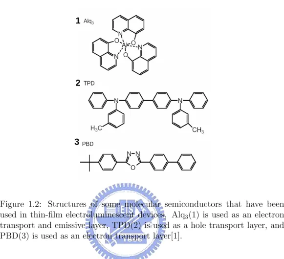
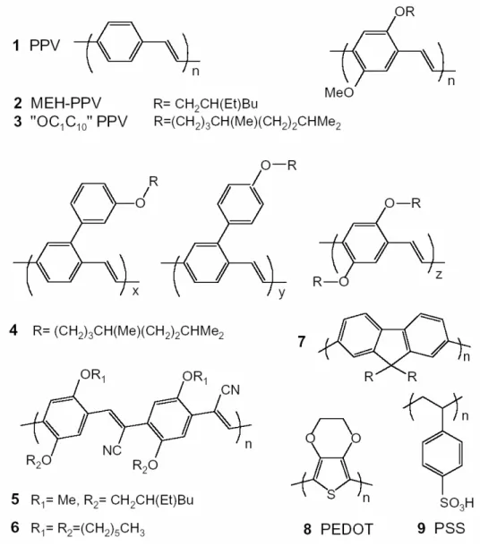
(10) List of Figures 1.1. 1.2. 1.3. 1.4. 1.5. The structure for silicon crystal is required for highly ordered arrangement for the atoms; the structure for the polymer chain has order for local area and disorder for global area. . . . . . . 3 Structures of some molecular semiconductors that have been used in thin-film electroluminescent devices. Alq3 (1) is used as an electron transport and emissive layer, TPD(2) is used as a hole transport layer, and PBD(3) is used as an electron transport layer[1]. . . . . . . . . . . . . . . . . . . . . . . . . . 4 Polymers used in electroluminescent diodes. The prototypical (green) fluorescent polymer is poly(p-phenylene vinylene), as shown by 1. Condensation polymerization of the bis(halomethyl) monomers affords the two best known (orange-red) solutionprocessible conjugated polymers MEH-PPV (2) and ”OC1 C10 ” PPV (3) which have been much used. Copolymers have been widely developed because they allow colour tuning and can show improved luminescence; copolymer 4 has recently been reported to show very high electroluminescence efficiency. Cyanoderivatives of PPV 5 and 6 show increased electron affinities and are used as electron transport materials. Poly(dialkylfluorene)s 7 is high-purity polymer, which show high luminescence efficiencies. ’Doped’ polymers such as poly(dioxyethylene thienylene), PEDOT (8), doped with polystyrenesulphonic acid, PSS (9), are widely used as hole-injection layers[1]. . . . . . . . . . 5 The molecular structures of (a) the first generation fac-tris(2-phenylpyridine) iridium cored dendrimer[2] and (b) a conjugated dendrimer consists of three parts: three distyrylbenzene chromophores surrounding a nitrogen core, meta-linked biphenyl units as dendrons and alkoxy groups as surface groups[3]. 6 (a)sp2 orbials and σ bonding for polyacetylene; (b) π orbitals and bonding for polyacetylene. . . . . . . . . . . . . . . . . . . 7 iii.
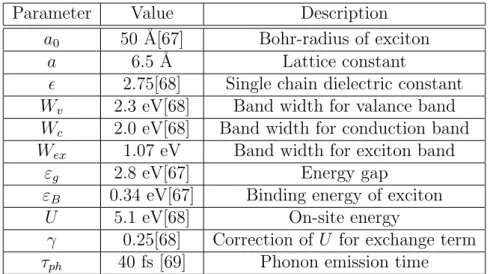
(11) iv. LIST OF FIGURES 1.6 1.7 1.8 1.9. 1.10. 1.11 1.12. 1.13 1.14 2.1. Schematic energy diagram for π-conjugated system: organic material which has σ and π bonding. . . . . . . . . . . . . . . 7 Spin singlet and triplet state. If the exciton formation is spinindependent, the singlet to triplet formation ratio is 1:3. . . . 9 The schematic energy structure for organic materials. . . . . . 9 The electric field dependence of hole and electron mobilities for MEH-PPV. The calculated mobilities (lines) are considering Poole-Frenkel form mobility[4]. . . . . . . . . . . . . . . . . . 11 Photoluminescence (PL), Electroluminescence (EL), and absorption (dashed line) spectra for a thin film of PPV, a typical conjugated organic polymer[5]. . . . . . . . . . . . . . . . . . . 12 Structure of a single-layer polymer LED (ITO/PPV/(Al, Mg, or Ca))[1]. . . . . . . . . . . . . . . . . . . . . . . . . . . . . . 13 Current density (solid line) and luminance (filled circles) for a 100 nm thick Pt/MEH-PPV/Ca device. The schematic energy diagrams below the plot illustrated device operation in equilibrium, reverse bias and in operation[6]. . . . . . . . . . . 14 Schematic of carrier injection processes at a metal / organic material interface[6]. . . . . . . . . . . . . . . . . . . . . . . . 15 Schematic energy diagram of the use of a heterojunction device to prevent holes from traversing the device without recombining[6]. 16. (a)Diagram for the direct Coulomb scattering term in which one conduction electron (c, ke , s) is captured by defect (d), while one free valence electron (v, −kf h , s0 ) is scattered to (v, −kh , s0 ). k is the wave number, and s is the spin index. (b)Diagram for the exchange Coulomb scattering term in which one valence electron (v, −kf h , s) is captured by defect, while one conduction electron (c, ke , s0 ) is scattered to the valence band state (v, −kh , s0 ). . . . . . . . . . . . . . . . . . . 25 2.2 Volume exciton dissociation rate cA (K) (see text) for defect Auger process is plotted as a function of the exciton centerof-mass wave number K for various defect level energy ∆ε measured from the midgap. The curves for ∆ε = −0.7 and −1.0 eV stop at K ≈ ±0.5π/a and ±0.3π/a, beyond which the energy released to the free hole exceeds the valence band width. . . . . . . . . . . . . . . . . . . . . . . . . . . . . . . . 32 2.3 Thermal averaged volume transition rates cA of defect Auger exciton dissociation, shown as a function of temperature. . . . 33.
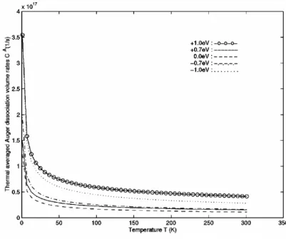
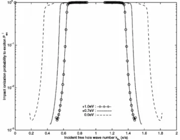
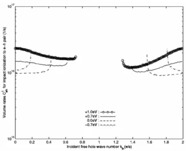
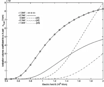
(12) LIST OF FIGURES 2.4. 2.5. 2.6 2.7 2.8. 2.9 2.10. 3.1. 3.2. 3.3. Dissociation probability P A (K) of an exciton passing through the defect is plotted as a function of center-of-mass wavenumber K of exciton. Rise at large K near the zone boundary is due to the smaller group velocity and longer interaction time. Volume transition rate cIex of defect impact ionization to exciton is shown as a function of incident hot hole momentum h ¯ kf h . All curves have threshold momentum required by the energy difference between the defect energy and the exciton energy. The curves of +1.0 eV, +0.7 eV and 0.0 eV stop at certain momenta, beyond which no final exciton state satisfies the energy conservation. This is because the exciton band width 1.1 eV is smaller than valence band width 2.3 eV for the incident free hole. . . . . . . . . . . . . . . . . . . . . . . . Probability for the defect impact ionization to exciton state by a hole which passes through the defect with momentum h ¯ kf h . I Volume transition rate ce−h of defect impact ionization to free electron-hole pair by an incident hole with momentum h ¯ kf h . . Impact ionization volume coefficient αV,ex by a hot hole to exciton under electric field E. The rate grows rapidly as the deep level energy deviation ∆ε goes from −1.0 eV to +1.0 eV. In order to distinguish them, we magnify curves for −1.0 eV, −0.7 eV and 0.0 eV by 5 times. . . . . . . . . . . . . . . . . . Impact ionization volume coefficient αV,e−h to free electronhole pair by a hot hole under electric field E. . . . . . . . . . . Volume coefficient αV,net for the net carrier generation due to impact ionization. αV,net is equal to αV,e−h − αV,ex because the former produces one more carrier and the latter neutralizes the incident hole itself. . . . . . . . . . . . . . . . . . . . . . .. v. 34. 35 36 37. 38 39. 40. The energy levels and relaxation channels for the singlet excitons (S1,S2) and triplet excitons (T1,T2) are shown. The decay from S2 and S1 is so fast that S2 → T2 transition can be neglected. Due to the large energy splitting between S1 and T1, the T1 → S1 transition is also neglected. . . . . . . . 46 Energy splitting and electron configuration for a metal ion with five d-electrons in octahedral ligand crystal field: (a) high spin, (b) low spin. . . . . . . . . . . . . . . . . . . . . . . . . 48 In the exchange interaction the Bloch electron in the polymer is scattered from k to k 0 with spin flip. There is a corresponding change in the magnetic quantum number of local moment from MS to MS0 = MS − 1. . . . . . . . . . . . . . . . . . . . . 50.
(13) vi. LIST OF FIGURES 3.4. The chemical structure and resonance integrals t, t1 , and t2 of PPV repeat unit are labeled. The relative position of the metal complex and the polymer is shown. The vertical distance between the ion nucleus and the polymer plane is 3.0 ˚ A. The orbitals for dxy , dxz , and dyz can stretch out of the ligands to interact with the pz orbit of the carbon atom on the polymer chain. . . . . . . . . . . . . . . . . . . . . . . . . . . 51. 3.5. The effect of the metal-polymer distance Rd on the strength of the exchange coupling is shown. Both the exchange integral and the resulting intersystem crossing rate wT 2S2 decrease exponentially as Rd increases due to reduced wavefunction overlap. For wT 2S2 the temperature is 300K, there is no energy splitting between S2 and T2 levels, and the total spin S of the metal ion is 5/2. . . . . . . . . . . . . . . . . . . . . . . . . . . 56. 3.6. The volume intersystem crossing rate wS1T 1 and wT 2S2 for various T2/S2 energy splitting ∆ES2T 2 are plotted as functions of temperature T . The total spin quantum number S for the metal ions is assumed to be 5/2. The actual transition rate is the volume rate times the number of dopant per repeat unit. wS1T 1 is independent of T because the T1/S1 energy splitting is much large than the thermal energy. . . . . . . . . . . . . . 57. 3.7. γT 2S2 and γS1T 1 have to be in the shaded region in order to raise the singlet formation ratio ηS . The straight lines A and B are mapped by changing the doping density Nd . Only in the case of line B there is a doping region for which the net effect of magnetic dopants is positive to the yield. . . . . . . . 59. 3.8. The singlet formation ratio ηS as the function of the doping density Nd for different ∆ES2T 2 . τT T is fixed at 3.7 ns. . . . . 61. 3.9. The singlet formation ratio ηS as the function of the doping density Nd for different T1 → T2 relaxation time τT T . ∆ES2T 2 is fixed at 0.01eV. Tighter triplet bottleneck (larger τT T ) redirects more triplet electron-hole pairs and causes higher singlet ratio. . . . . . . . . . . . . . . . . . . . . . . . . . . . . . . . 61. 3.10 The singlet formation ratio ηS is shown for various metalpolymer distance Rd . It is easier to enhance the singlet formation when Rd is smaller and the exchange coupling is stronger. The physically relevant range for Rd is between 3 and 3.5 ˚ A. . 62 4.1. Schematic of single layer LED structure[6]. . . . . . . . . . . . 69.
(14) LIST OF FIGURES 4.2. Single Carrier Device Operation. The asymmetry of the current voltage curve is due to the difference in Schottky energy barriers to injection of holes, shown in the energy diagrams[6].. vii. 70. 4.3. Energy diagram illustrating transport and injection in a hole only device[6]. . . . . . . . . . . . . . . . . . . . . . . . . . . . 71. 4.4. Schematic of localized density of states in organic materials[6]. 73. 4.5. Current processes at the metal / organic interface[6]. . . . . . 74. 4.6. Schematic of an organic LED showing complete recombination (left) and incomplete recombination (right)[6]. . . . . . . . . . 77. 4.7. The gridding scheme used for the device model. N are grid points, M are half grid points[6]. . . . . . . . . . . . . . . . . . 79. 4.8. The current voltage characteristics are obtained by applying a series of voltage ramps in time to the right electrode[6]. . . . 82. 4.9. Carriers tunnel through a triangular barrier which includes image force lowering[6]. . . . . . . . . . . . . . . . . . . . . . . 83. 4.10 The structure of two hole-only device: (a) real hole-only device with two high work function metals on the two contact; (b) effective hole-only device with one high work function metal on the right contact and one low work function metal on the left contact. . . . . . . . . . . . . . . . . . . . . . . . . . . . . 84 4.11 The electric fields profiles for the two hole-only devices in fig. 4.10:(a) is for standard device in fig. 4.10(a); (b) is for effective device in fig. 4.10(b); (c) is the potential for the standard device. 86 4.12 The electron (dashed line) and hole (solid line) density profiles for the two hole-only devices in fig. 4.10: (a) is for standard device in fig. 4.10(a); (b) is for standard device in fig. 4.10(b). 87 4.13 The recombination rate profiles for the two hole-only devices in fig. 4.10: (a) is for standard device in fig. 4.10(a); (b) is for standard device in fig. 4.10(b). . . . . . . . . . . . . . . . . . . 89 4.14 The structures of double carrier device with (a) symmetric carrier mobility and (b) Asymmetric carrier mobility. . . . . . 90 4.15 The electric fields profiles for the two double carrier devices in fig. 4.14: (a) is for symmetric device in fig. 4.14(a); (b) is for asymmetric device in fig. 4.14(b). The profiles variation for voltage as 3V (dotted line), 6V (dashed line), and 10V (solid line) are presented; (c) is the potential for the symmetric case. 91.
(15) viii. LIST OF FIGURES 4.16 (a) The electron (dashed line) and hole (solid line) density profiles for the symmetric double carrier device in fig. 4.14(a); (b) the electron and (c) hole density profile for the asymmetric double carrier device in fig. 4.14(b). The profile variation for voltage as 3V (dotted line), 6V (dashed line), and 10V (solid line) are presented in (b) and (c). . . . . . . . . . . . . . . . 4.17 The recombination rate profiles for the double carrier devices in fig. 4.14: (a) is for symmetric device in fig. 4.14(a); (b) is for asymmetric device in fig. 4.14(b). The profile variation for voltage as 3V (dotted line), 6V (dashed line), and 10V (solid line) are presented in (b). . . . . . . . . . . . . . . . . . . . 4.18 Gridding scheme for device model of multilayer devices. N labels gridpoints, and M labels half-gridpoints[6]. . . . . . . 4.19 Schematic of the boundary conditions used at the heterojunction. . . . . . . . . . . . . . . . . . . . . . . . . . . . . . . . 4.20 The structures of the double carrier bilayer devices with (a) symmetric and (b) asymmetric carrier mobility. . . . . . . . 4.21 The electric fields profiles for the two double carrier bilayer devices in fig. 4.20: (a) is for symmetric device in fig. 4.20(a); (b) is for asymmetric device in fig. 4.20(b). The profiles variation for voltage as 3V (dotted line), 6V (dashed line), and 10V (solid line) are presented. . . . . . . . . . . . . . . . . . 4.22 (a) The electron (dashed line) and hole (solid line) density profiles for the symmetric double carrier bilayer device in fig. 4.20(a); (b) the electron and (c) hole density profile for the asymmetric double carrier bilayer device in fig. 4.20(b). The profile variation for voltage as 3V (dotted line), 6V (dashed line), and 10V (solid line) are presented in (b) and (c). . . . 4.23 The recombination rate profiles for the double carrier bilayer devices in fig. 4.20: (a) is for symmetric device in fig. 4.20(a); (b) is for asymmetric device in fig. 4.20(b). The profile variation for voltage as 3V (dotted line), 6V (dashed line), and 10V (solid line) are presented in (b). . . . . . . . . . . . . . 4.24 The device structures for varying the electron energy barrier between the green and blue layers, ∆ΦeGB , and the blue and electron blocking layer, ∆ΦeBE . As varying ∆ΦeGB from 0.1eV to 0.3eV, ∆ΦeBE is kept as 0.3eV. As varying ∆ΦeBE from 0.1eV to 0.6eV, ∆ΦeGB is kept as 0.1eV. . . . . . . . . . . . 4.25 The recombination rate profiles for the device varying (a) ∆ΦeGB and (b) ∆ΦeBE . . . . . . . . . . . . . . . . . . . . . .. . 93. . 94 . 95 . 96 . 99. . 100. . 101. . 103. . 105 . 107.
(16) LIST OF FIGURES. ix. 4.26 The recombination ratios as functions of (a) ∆ΦeGB and (b) ∆ΦeGB . . . . . . . . . . . . . . . . . . . . . . . . . . . . . . . 108 4.27 The device structures for varying the ratio of the electron zero field mobility to the hole zero field mobility for the green layer, mG , and for blue layer, mB . mG ranges from 1.0, 0.1, 0.01, and to 0.001; mB ranges from 0.2, 0.1, 0.05, and to 0.025. . . . 109 4.28 The recombination rate profiles for the device varying (a) mG and (b) mB . . . . . . . . . . . . . . . . . . . . . . . . . . . . . 110 4.29 The recombination ratios as functions of (a) mG and (b) mB . . 111 4.30 The structures for the devices varying layer thickness of the green layer (LG ) and the blue layer (LB ). . . . . . . . . . . . . 112 4.31 The recombination rate profiles for varying the layer thickness (a) LG and (b) LB . . . . . . . . . . . . . . . . . . . . . . . . . 113 4.32 The recombination ratios for varying the layer thickness (a) LG and (b) LB . . . . . . . . . . . . . . . . . . . . . . . . . . . 114 4.33 The structures of two color-tuning devices. Device A has a faster electron mobility for the green layer than that of the other layer. Device B has a thicker green layer (50nm and ) and thinner blue layer (20nm). . . . . . . . . . . . . . . . . . . 115 4.34 The (a) electron density, (b) the hole density, and (c) the recombination rate profile for the device A in Fig. 4.33. . . . . 116 4.35 The continuous motion of the CIE coordinates for device A (small open circle) and B (dashed line). The inset shows relative recombination ratio of each layer for device A (green: open circle; blue: open diamond) and B (green: dashed line; blue: dotted line). The three stars labelled with ”Red”, ”Green”, and ”Blue” are defined by the phosphors of the typical red, green, and blue color monitor plots. The large open circle label;ed with ”White” is where the white color area is. The small black triangle beside ”Red” star is the position for the spectrum peak of the red layer, the small black square is for that of the green layer, and the small black diamond is for that of the blue layer. . . . . . . . . . . . . . . . . . . . . . . . 118 4.36 (a)Device structure for multilayer diode: PF(G)(60nm)/PF(R)(10nm)LiF(6nm); (b)Spectra for upper device[7]. . . . . . . . . . . . . 119 4.37 (a)Device structure for multilayer diode: PF(B)+DPOC1 0(60nm)/PF(R)(10nm)LiF(6nm); (b)Spectra for upper device[7]. . . . . . . . . . . . . 120 4.38 (a)Device structure of multilayer LED, (b)chemical structure of the emissive polymers DP10-PPV, and (c)BEHF. (d) The EA and IP are also shown. . . . . . . . . . . . . . . . . . . . . 122.
(17) x. LIST OF FIGURES 4.39 (Color)(a)Normalized spectra and (b)pictures of triple-layer device A(BGR) at various voltage. . . . . . . . . . . . . . . . 123 4.40 (a)Current-voltage and (b) luminescence-voltage relations for devices A-D. . . . . . . . . . . . . . . . . . . . . . . . . . . . . 124 4.41 (a)Normalized spectra of triple-layer device B(BGR) and of (b)double-layer device C(BG) (c) D(GB). Green emission is normalized. . . . . . . . . . . . . . . . . . . . . . . . . . . . . 126.
(18) List of Tables 1.1 1.2 1.3. Device specifications for the luminescence materials of OLED[8]. 19 Device specifications for the phosphorescence materials of OLED[8]. 20 Device specifications for the luminescence materials of PLED[8]. 21. 2.1. All parameters, suitable for PPV, used in the calculations are listed with references given after the values. . . . . . . . . . . 31. xi.
(19) xii. LIST OF TABLES.
(20) Chapter 1 Introduction to Organic Luminescent Semiconductors. 1.
(21) 2. CHAPTER 1. INTRODUCTION. Optoelectronic devices based on organic materials have attracted much attention since the demonstration of the efficient organic light emitting diodes (LEDs) by Tang and van Slyke in 1987, and the first polymer LEDs by Friend in 1990[9, 10]. Their ease of fabrication processes and applicability to flexible and curved substrates, and prospect for much lower cost than their counterpart of inorganic semiconductors make them good candidates for novel flat panel displays which would resolved some severe difficulties for flat panel display based on liquid crystal[11–13]. The ideal display has high brightness, high power efficiency, and low cost[11, 14, 15]. Organic LEDs have promised for satisfying these requirements, making a better understanding of their operation principles very desirable. This chapter provides some fundamental knowledge to organic LEDs. First, the materials properties of conjugated organic materials is presented. Then the basic operation principles of organic LED devices are discussed. The latest technological status of organic LEDs is reviewed concisely. Finally, with three research topics included in this dissertation, the motivation and structure for each topic, and the mutual relations among them are explained.. 1.1. Material properties of conjugated polymer. Inorganic materials are comprised with silicon, however organic materials are made from carbons. The most important difference between inorganic and organic materials is that inorganic materials are ”ordered system”, however organic materials are ”disordered”(Fig. 1.1). This chapter deals with the materials properties of organic materials used for optoelectronic devices. Some common organic material, small molecule, polymers, and conjugated dendrimers, are shown in Figs. 1.2, 1.3 and 1.4 [1–3, 15]. First the electronic structure of organic materials will be presented, followed by their transport, and finally optical properties.. 1.1.1. Electronic structure. The organic materials for organic LEDs are intrinsic semiconductors with large energy gap[16, 17]. The electronic structure of π-conjugated organic semiconductors differs from that of crystalline inorganic semiconductors. The inorganic semiconductor forms a rigid crystalline network, and it is the extended network to determine the electronic structure. The termination of a crystal leads to surface states which lie in the gap and have an effect on.
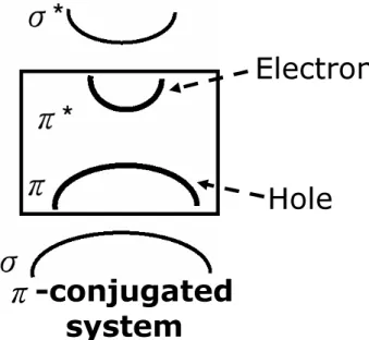
(22) 1.1. MATERIAL PROPERTIES. Silicon. 3. Polyacetylene film. Figure 1.1: The structure for silicon crystal is required for highly ordered arrangement for the atoms; the structure for the polymer chain has order for local area and disorder for global area. device behavior[18]. The π-conjugated organic has an electronic structure which is basically determined by the conjugation lengths of the polymer or organic molecule[14, 19]. Although such states may arise because of chemical bonding with deposited metals or other organic materials, in general, there is fundamentally no reason for surface states in an organic material. But here are still deep levels states lying in the gap due to other reasons, eg. oxidation, for organic materials [20–22]. Owing to severe electron trapping, electron transport demonstrate trap limited behavior[23–25]. Conjugated organics consist of chains of carbons with alternating double and single bonds(Fig. 1.5(a)). The structural bonding arises from overlap of sp2 hybridized orbitals which have a strong interaction similar to the overlap of the sp3 orbitals and form σ bonds with a bonding antibonding orbital splitting of about 10 eV, however in these materials the conduction arises from the overlap of π orbitals to form π bonds which have a weaker interaction and consequently a smaller bonding antibonding orbital splitting (Fig.1.5(b)). The three sp2 orbitals are coplanar and separated by 120◦ . The π orbitals are perpendicular to this plane. The σ bonding by sp2 orbitals from adjacent carbons forms a ”planar” backbone, with the conduction π orbitals perpendicular to this plane and therefore having a smaller overlap. The single bonds in the conjugated system consist of a σ bond, the double bonds consist of a σ bond, and a π bond. Fig. 1.6 illustrates the the energy levels for π-conjugated system. The energy level correspond to the electronic energy levels of electrons or holes.
(23) 4. CHAPTER 1. INTRODUCTION. 1. 2. 3. Figure 1.2: Structures of some molecular semiconductors that have been used in thin-film electroluminescent devices. Alq3 (1) is used as an electron transport and emissive layer, TPD(2) is used as a hole transport layer, and PBD(3) is used as an electron transport layer[1]. on a rigid organic molecule or conjugated segment of polymer. Each of these electronic levels consists of many levels due to the vibrational and rotational energy of the host molecule. There are defect levels, notably carbonyls introduced by photo-oxidation of the vinylene bond, which have been shown to lie in the π-π* gap and degrade performance of polymer light emitting devices[26]. Not all defects lie in the π-π* gap, and only those that do require attention to prevent them from degrading device performance[15]. When a charge is added to a conjugated organic segment, it induces a structural relaxation of organic, so that the energy levels for electrons and holes shift to lower energies than those given for a rigid molecule[27]. This energy shift is estimated to be 50 meV to 100 meV in organics, compared to a shift of 2meV in GaAs[28, 29]. Because of this relaxation the fundamental charge particle on a segment is not a electron or hole, but rather the quasiparticles which include the electron and the structure deformation it induces or the hole and the structural deformation it induces. These particles are called electron polarons and hole polarons. Since all charge carriers discussed in this work are either electron polarons or hole polarons, they are.
(24) 1.1. MATERIAL PROPERTIES. 5. Figure 1.3: Polymers used in electroluminescent diodes. The prototypical (green) fluorescent polymer is poly(p-phenylene vinylene), as shown by 1. Condensation polymerization of the bis(halomethyl) monomers affords the two best known (orange-red) solution-processible conjugated polymers MEHPPV (2) and ”OC1 C10 ” PPV (3) which have been much used. Copolymers have been widely developed because they allow colour tuning and can show improved luminescence; copolymer 4 has recently been reported to show very high electroluminescence efficiency. Cyano-derivatives of PPV 5 and 6 show increased electron affinities and are used as electron transport materials. Poly(dialkylfluorene)s 7 is high-purity polymer, which show high luminescence efficiencies. ’Doped’ polymers such as poly(dioxyethylene thienylene), PEDOT (8), doped with polystyrenesulphonic acid, PSS (9), are widely used as hole-injection layers[1]..
(25) 6. CHAPTER 1. INTRODUCTION. (a) RO. OR R. OR RO. OR. (b). RO. OR. R=. RO. OR. Figure 1.4: The molecular structures of (a) the first generation fac-tris-(2phenylpyridine) iridium cored dendrimer[2] and (b) a conjugated dendrimer consists of three parts: three distyrylbenzene chromophores surrounding a nitrogen core, meta-linked biphenyl units as dendrons and alkoxy groups as surface groups[3]..
(26) 1.1. MATERIAL PROPERTIES. sp2 Ӻbond. 7. (a). (b). Polyacetylene Figure 1.5: (a)sp2 orbials and σ bonding for polyacetylene; (b) π orbitals and bonding for polyacetylene.. Electron Hole Ӹ-conjugated system Figure 1.6: Schematic energy diagram for π-conjugated system: organic material which has σ and π bonding..
(27) 8. CHAPTER 1. INTRODUCTION. denoted simply as electrons and holes, the polaronic nature being implicit. The energy levels of the electron and hole polarons form the energy levels for conduction. The conduction is dominated by the highest of the filled energy states and the lowest of the empty energy states. The highest energy of the full states is called the valence energy level on this work, denoted EV , in chemistry it is called the highest occupied molecular orbital or HOMO. The lowest energy of the empty states is called the conduction energy level in this work, denoted EC , in chemistry it is called the lowest unoccupied molecular orbital or LUMO.. In organic material, an electron and a hole form a electron-hole pair, the energy for the pair is just the summation for one electron energy and one hole energy. If the distance between them is close enough for the pair to feel the coulomb force for each other, they could form ”exciton” state. The energy for an exciton state is lower than that of electron-hole pair by a negative attractive potential due to the Coulomb interaction, which is called exciton ”binding energy”. Another important difference between inorganic and organic materials is that the exciton binding energy for the organic material is much larger ( 0.4eV)[30] that for the inorganic material, which ia about several meV. A binding energy of 0.4eV is equivalent to thermal energy for the case of temperature of 4641K, hence under room temperature, the exciton state is very stable, which will not be excited to be dissociated by thermal energy. An exciton state is a ”hydrogen-like” state[15], hence the energy level for exciton state has familiar structure as hydrogen atom. There are four kinds of spin states for exciton formation(Fig. 1.7). The exciton spin state with spin angular momentum 0 is called ”singlet” exciton, that with spin angular momentum 1 is called ”triplet’ exciton. Because there are one kind of singlet state and three kinds of triplet state, if the exciton formation is spin-independent, the formation ration for singlet and triplet exciton will be 1:3. Absorbing and emitting one photon can not violate the spin angular momentum conservation: ∆S = 0. The ground state and the singlet exciton is singlet state, the transition between them obeys the dipole selection rule, so the singlet state is radiative. The triplet exciton is triplet state, the transition between the ground state and the triplet exciton state violates the dipole selection rule, so the triplet is nonradiative. Due to exchange interaction[31], there is an large energy difference ( 1.0eV) between the lowest singlet and triplet state, but the exchange energy between the second lowest singlet and triplet state is around 0.01eV to 0.1eV (Fig. 1.8)..
(28) 1.1. MATERIAL PROPERTIES. 9. Spinindependent 1:3. Singlet exciton. Δ. Triplet exciton. Figure 1.7: Spin singlet and triplet state. If the exciton formation is spinindependent, the singlet to triplet formation ratio is 1:3.. Free carrier continuum 3/4. 1/4 S2 S1. T2 ӻsg~1ns. T1 ӻtg~1ms. Ground state Figure 1.8: The schematic energy structure for organic materials..
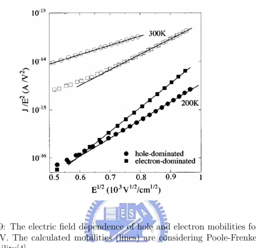
(29) 10. 1.1.2. CHAPTER 1. INTRODUCTION. Transport properties. So far the energy picture for a single conjugated segment has been presented. The energy diagram appropriate for the description of conduction through this single segment would consist of the two levels EC and EV . Now bring together a large number of these segments to form a solid and consider an electron traversing this solid. Motion along the conjugated segments (intrachain motion) is much easier than the traverse from one segment to another (interchain motion). The ease of this motion depends on how well the π orbitals of the two segments overlap, the distance between the segments, and the energy difference between the conduction levels. The difficult interchain hopping forms the rate limiting step which determines the transport properties. The energy levels of the different segments vary due to distribution in conjugated length, stresses caused by the packing, fluctuations in density or other local environmental factors. Because of this variation, the transport is by hopping through manifolds of localized states which have some random energetic distribution[32–34]. The transport in conjugated organic materials has been studied by a variety of methods. Transient methods include time of flight (TOF), and time resolved current measurements[24, 35–37]. Steady state current voltage characteristics of organic diodes have also been used to determine carrier transport.[38–40]. Many such experiments on different organic materials and systems conclude that the carrier mobilities are strongly field dependent (Fig. 1.9). A possible theoretical description of the physical process leading to this field dependence has been given based on hopping conduction through a distribution of localized states[32–34]. This is the model for transport used in this work. Others describe the transport as trap and release of constant mobility carriers by a distribution of localized trapping states[41, 42]. These two pictures are likely just alternative expressions of the same physical phenomena[43].. 1.1.3. Optical properties. Two methods of characterizing the optical properties of materials are by their absorption and photoluminescence spectra[15]. The absorption of a photon leads first to an exciton on a molecule, the exciton then relaxes to its lowest energy state as the molecular structure relaxes. the exciton then diffuses to the lowest energy state available before it recombines. Thus there is a splitting of the absorption and emission spectra because absorption of photons leads to excitons on an unrelaxed molecules, whereas emission is from lower energy excitons on relaxed molecules. The emission spectrum of a single molecule has lower energy than the absorption spectrum of the same.
(30) 1.2. ORGANIC LIGHT EMITTING DIODE (LED). 11. 3. Figure 1.9: The electric field dependence of hole and electron mobilities for MEH-PPV. The calculated mobilities (lines) are considering Poole-Frenkel form mobility[4]. molecule, and has a width which is a measure of the width of the vibrational and rotational states of the molecule. The absorption spectrum is broader because transitions are possible from occupied states in the valence levels to unoccupied states in the conduction level, rather than just from the lowest energy exciton state. In a solid the spectra are broadened further by the distribution of localized states. The emission is now from the lowest energy exciton state in the local region accessible to the the exciton in its lifetime, whereas the absorption is from any full state to any empty unrelaxed state. The emission and absorption spectra are shown in Fig. 1.10 for PPV, a typical conjugated polymer[5].. 1.2. Organic Light emitting diode (LED). The first efficient organic LEDs were reported in 1987, and the first polymer LEDs were reported in 1990[9, 10]. In 1991 the improvement of the injecting electrodes was reported for polymer LEDs[44]. The electronic and optical.
(31) 12. CHAPTER 1. INTRODUCTION. Figure 1.10: Photoluminescence (PL), Electroluminescence (EL), and absorption (dashed line) spectra for a thin film of PPV, a typical conjugated organic polymer[5]. properties of organic LEDs can be varied over wide ranges depending on their chemical composition. Organic molecules interact by weak van der Waals interactions and are relatively insensitive to the nature of the substrate they are deposited on. Polymers can be solution deposited by spin casting or ink jet printing, permitting large area deposition, and substantially lower production costs. Processing temperatures are low, allowing the use of thin, flexible and cheap plastic substrates[14, 15]. The simplest organic LED is a single layer of organic material (PPV) sandwiched between two electrodes as illustrated in Fig. 1.11[15]. The injection of carriers is determined by the barrier between the metal fermi level and the carrier energy level in the organic. For small barriers the contact is easily able to supply carriers, and current is determined by the bulk transport properties of organic material. This is the space charge limited regime[25]. If the barrier is sufficient large, then the organic is able to transport carriers more efficiently than the contact can inject them, and the current is determined by the processes at the contact. This is the contact limited regime. For organic LEDs the contacts are chosen so that one contact can easily inject electrons, and the other can easily inject holes into the organic material. Large work function metals such as platinum or gold are better hole injectors, whereas low work function metals such as calcium or magnesium are better electron.
(32) 1.2. ORGANIC LIGHT EMITTING DIODE (LED). 13. Figure 1.11: Structure of a single-layer polymer LED (ITO/PPV/(Al, Mg, or Ca))[1].. injectors. When a suitable voltage bias is applied across the device the contacts are able to inject holes and electrons into polaron states. The electron and hole polarons drift across the device, and if they meet can form an exciton which may recombine radiatively. If the opposite bias is applied, so that holes are drawn from the contact which easily injects electron, and electrons from the contact which easily injects holes, then essentially no current flows through the device, and no light is emitted. This is illustrated in Fig. 1.12. The physical processes of interest in an organic LED are injection of carriers at the contacts, transport of carriers across the device, and recombination of carriers in the device[19, 40, 45]. The injection is from the metal into the distribution of localized conduction or valence states. The injection processes, illustrated in Fig. 1.13, are: thermionic emission from the metal into the distribution of localized states in the organic; the time reversed process of thermionic emission which is a backflowing current from the organic material into the contact; and tunneling of carriers from the metal into the organic. Image force lowering of the barrier to injection must be taken into account. It has been shown that for devices of interest tunneling is negligible, and further that thermionic emission and its time reversed process are nearly equal and much larger than the device current at the injecting contact, so that quasithermal equilibrium is established at that contact[45]. This is a nice result because it means that the device characteristics are determined by the quasithermal equilibrium carrier densities at the contact, and the specific forms for the injecting and backflowing current which establish this quasithermal.
(33) CHAPTER 1. INTRODUCTION. Luminance (mW/cm2). Current Density (A/cm2). 14. Voltage (V) e Ec Ef. Ev reverse bias. h equilibrium. in operation. Figure 1.12: Current density (solid line) and luminance (filled circles) for a 100 nm thick Pt/MEH-PPV/Ca device. The schematic energy diagrams below the plot illustrated device operation in equilibrium, reverse bias and in operation[6]..
(34) 1.2. ORGANIC LIGHT EMITTING DIODE (LED). 15. energy Backflow Thermionic emission. Image force lowering. Tunneling. Metal. Organic material. x Figure 1.13: Schematic of carrier injection processes at a metal / organic material interface[6]. equilibrium are not important. The energy barrier to injection is very important in determining the injection. These barriers have been measured for a variety of systems. The energy barriers for a variety of metals contacting the polymer MEH-PPV were measured using internal photoemission and electroabsorption and found to follow the ideal Schottky picture[46]. Using these same techniques, the energy barriers for a variety of metals contacting the molecular organic Alq3 has been studied and found to only follow the ideal Schottky picture in some cases[38]. UPS studies of the molecular organic PTCDA on titanium, gold, and indium, show that interface reactions are possible which could destroy the ideal Schottky picture[21, 22]. The transport of carriers across the device through the distribution of localized states is described by a field dependent mobility of the form seen in time of flight measurements. The theory for carrier recombination in low carrier mobility materials has been investigated previously[47, 48]. The result is a bimolecular recombination rate with a Langevin form for the kinetic coefficient. The physical model in organic is of two polarons moving towards each other under the influence of their mutual coulomb attraction and forming an exciton when they meet which quickly recombines. Multilayer devices are useful for improving the efficiency of organic LEDs when the organic material chosen for emission layer has certain characteris-.
(35) 16. CHAPTER 1. INTRODUCTION. e. e. h h. h. hole pass through. hole blocked. Figure 1.14: Schematic energy diagram of the use of a heterojunction device to prevent holes from traversing the device without recombining[6]. tics that make single layer devices inefficient[14, 15]. These characteristics could be the inability to make space charge limited contact for injection of one or both carriers, or poor transport properties for one or both carriers. The problems that these characteristics can cause in a single layer device are incomplete recombination of one carrier, carrier recombination very near a metal contact where nonradiative losses can occur, and high drive voltages needed to obtain a given light output. Multilayer devices address this problems by including carrier blocking layer to prevent carriers from traversing the device without recombining, or to locate recombination away from the contact, and by electron or hole transport layers which lower the required voltages needed for a given light output. The use of a multilayer device to prevent holes from traversing a devices is illustrated schematically in Fig. 1.14. The physical precesses of concern here are again charge injection from the contacts, charge transport through the organic layers, and carrier recombination in the device, however now charge injection processes at the heterojunction must also be considered. Then injection processes considered at the heterojunction are thermionic emission and its time reversed process, however the barrier lowering and tunneling do not occur.. 1.3. Present status for organic LED. The current technological status of organic LEDs are as follows[1, 11, 15]. Single layer polymer LEDs have been reported with external quantum efficiency of about 2%. Multilayer molecular based LEDs have been reported with external quantum efficiency of about 4%. With fluorescence combined with top emission,[49] external quantum efficiency of from 5% to 8% are achievable[50, 51]. The very highest efficiencies are accesible only through the use of electro-phosphorescence, which allows for 100% of the injected.
(36) 1.3. PRESENT STATUS FOR ORGANIC LED. 17. electron-hole pairs to result in emissive triplet exciton[52, 53]. OLEDs based on small molecular weight metallorganic iridium complexes have internal quantum efficiency approaching 100%, resulting in 20-40% external efficiency, depending on whether substrate or top emission schemes are employed[54, 55]. Phosphorescence has not been fully exploited in polymer based systems, significant progress in this direction has been made recently in demonstrating high efficiency red, green, and blue triplet emission in modified forms of poly(vinylcarbazole). The highly external quantum efficiencies of 5.5%, 9%, and 3.5% in respective red, green, and blue PLEDs were achieved by selecting the electron transport material for the emissive layer and optimizing the content of the iridium-complexes unit in the phosphorescent polymer chain[56]. For display applications more useful metrics are power efficiency and luminance. Extremely rapid advances in OLED efficiencies have been made since the early 1990s, with peak efficiencies of 70 (10, 8) lm/W in the green (red, blue) for molecular PHOLEDs (Phosphorescent OLEDs). The operational lifetime of electrophosphorescent devices is as long as, or even exceeds that of fluorescent OLEDs, thereby meeting the needs of many current display platforms[57]. Single layer polymer LEDs with yellow/green emission have been reported with luminous efficiencies of about 2lm/W, peak brightness in excess of 5 × 10⁶ cd/m2 , lifetimes at 100 cd/m2 exceeding 1400 hours, and drive voltages below 4V required for brightness of 100 cd/m2 [58]. For multilayer based LEDs luminous efficiencies of about 15 lm/W have been reported for green LEDs. The highest luminances obtained are 105 cd/m2 , about 3 order brighter than a computer screen. Estimated lifetimes exceeding 50000 hours for a brightness of 100 cd/m2 have been reported.[14]. Progress in white OLEDs has continued apace, with the highest PHOLED efficiencies reported near 15 lm/W, comparable to that of an unfiltered incandescent lamp[59]. An external quantum yield of 4.5% for white emission in PLED by using blue-phosphorescent and red-phosphorescent polymers was obtained[56]. Note that the OLED efficiencies are measured for devices on flat glass substrates, where the total out-coupling is only 20%. This is compared to ultra-high brightness inorganic AlInGaP red LEDs, where nearly all emitted light is projected into the viewing direction, leading to external efficiencies approximately equal to their internal efficiencies. Tables. 1.1, 1.2, and 1.3 demonstrate comparisons for the characteristics of performance for the luminescence materials for OLED, the phosphorescence materials for OLED, and the luminescence materials for PLED respectively around two years ago. Although the data are not all updated results for these devices, the trends for the power efficiencies and the lifetime are.
(37) 18. CHAPTER 1. INTRODUCTION. still the same. The power efficiency of the green material for these devices are the highest, and that of the red and blue materials are all much lower. The reason for this result is that the sensitivity to light for human eyes is a function of the wave length of the light. The sensitivity strength for the green light is the highest, say 100%, and that for the red and blue light are lower than that for the green, say 35% and 10% respectively. The efficiency for the green material meets the requirement for commercialization, however much labor is needed to be paid to the efficiencies improvement for the red and blue color material. Lifetime for the red light material is longer than that of the green the blue materials. The exact mechanism for this lifetime difference among these materials is still a puzzle. One possible reason for this lifetime difference is the energy gap difference for these materials. In principle, the materials with larger energy gap can transfer more energy into radiations and heats. The heats may cause some chemical interactions for the material, which will make the ability for the transport and the light emission of the materials decaying.. 1.4. The structure of this dissertation. Chapter 2 of this dissertation starts from the process on dark current induced by photo-excited below bandgap. Auger exciton dissociation through deep level defects was proposed as the possible mechanism. The inverse process of Auger process, impact ionization, was calculated also. A feasible electroluminescence for unipolar light-emitting diode based on the impact ionization process is presented[60]. Chapter 3 presents a method to improve electroluminescence efficiency of conjugated polymer LED theoretically. Doping magnetic complexes into polymer LED can turn on the transition channel between radiative singlet exciton and nonradiative triplet exciton. With suitable concentration for the doped magnetic complexes, it is possible for the singlet exciton ratio being up to 80% higher than 25% for the spin independent value[61]. Chapter 4 shows device simulation for multilayer organic light-emitting diode. Some structures are shown to have possibility to tune the luminescence color from red, green, then to blue as bias voltage increasing. These structures provide some possible solutions for full-color display with organic material other than the common technology by ink-jet printing method[62]..
(38) 1.4. THE STRUCTURE OF THIS DISSERTATION. Color. R. G. B. 19. Characteristics. Kodak 2001. Pioneer 2002. IDEMITSU 2002. Efficiency. 6 cd/A. 2.6 cd/A. 3.5 cd/A. CIE. (0.67,0.33). (0.62,0.38). (0.64,0.36). Lifetime. 35,000 hrs @5mA/cm2. 10,000 hrs @250 nits. 10,000 @500 nits. Efficiency. 15 cd/A. 16 cd/A. --. CIE. (0.25,0.62). Lifetime. 12,000 hrs @5mA/cm2. 10,000 hrs @300 nits. --. Efficiency. 3.5 cd/A. 3.9 cd/A. 4.7 cd/A. CIE. (0.15,0.15). (0.14,0.12). (0.15,0.17). Lifetime. 12,000 hrs @5mA/cm2. 10,000 hrs @100 nits. 10,000 hrs @200 nits. --. Luminescence for OLED Table 1.1: Device specifications for the luminescence materials of OLED[8]..
(39) 20. CHAPTER 1. INTRODUCTION. color. R. Characteristics. UDC 2001. Pioneer. Efficiency. 8.2 cd/A. 3.2 cd/A. CIE. (0.65,0.34). (0.66,0.32). Lifetime. 5000 hrs @ 300 nits. 30,000 hrs @ 135 nits. Efficiency. 29 lm/W. 59 cd/A. 25 cd/A. CIE. (0.30,0.63). (0.30,0.64). (0.30,0.63). Lifetime. > 50,000 hrs. < 1000 hrs @500 nits. 3300hrs @818 nits. Efficiency. 6.3 lm/W. --. CIE. (0.16,0.29). --. Lifetime. < 1000 hrs. --. G. B. Phosphorescence for OLED Table 1.2: OLED[8].. Device specifications for the phosphorescence materials of.
(40) 1.4. THE STRUCTURE OF THIS DISSERTATION. Color. R. G. B. W. 21. Characteristics. CDT 2001. Dow 2001. Covion 2002. Efficiency. 2.3 lm/W @100 nits @2.4V. 1 lm/W. 1.6 cd/A. CIE. (0.68,0.31). (0.67,0.33). (0.67,0.33). Lifetime. > 50,000 hrs. 10,000 hrs @100 nits. >10,000 hrs @70 Nits. Efficiency. 15 lm/W @100 nits @2.7V. 15.7 lm/W. 14 cd/A. CIE. (0.39,0.58). (0.39,0.56). (0.32,0.60). Lifetime. ~ 10,000 hrs. >10,000 hrs @90 Nits. --. Efficiency. 2.5 lm/W @100 nits @3.5V. 0.4 lm/W. 2.7 cd/A. CIE. (0.16,0.14). (0.22,0.27). (0.15,0.12). Lifetime. > 2,500. --. 10,000 hrs @200 nits. Efficiency. 1.5 lm/W @100 nits @4.3V. --. ~ 7 cd/A. CIE. --. --. (0.34,0.40). Lifetime. > 7,000 hrs. --. --. Luminescence for PLED Table 1.3: Device specifications for the luminescence materials of PLED[8]..
(41) 22. CHAPTER 1. INTRODUCTION.
(42) Chapter 2 Defect Auger exciton dissociation and impact ionization in conjugated polymers. 23.
(43) 24CHAPTER 2. EXCITON DISSOCIATION AND PHOTOCONDUCTIVITY. 2.1. Exciton dissociation and generation by deep level defects. The past ten years has witnessed a tremendous progress in both the science and technologies of light-emitting devices based on conjugated polymers[1]. Yet many fundamental questions regarding the two single important properties, electroluminescence (EL) and photoconductivity (PC), remain unanswered. The defects in the polymer chain, either structural or chemical, are believed to play an important role in both EL and PC. The deep electronic levels associated with the defects provide a convenient way to facilitate the dissociation of the exciton, and limit the luminescence quantum yield in EL. On the other hand, excitons must be dissociated in order to produce charge carriers for PC for excitation below the continuum threshold[63]. Even though the enhancement of PC and reduction of EL by oxidation, presumably due to exciton dissociation at the carbonyl defects, has been reported experimentally[24], the microscopic mechanism which controls the dissociation rate is not well understood. A new exciton dissociation mechanism, the defect Auger process, is studied in this work. In this process the electron (hole) in the exciton drops into the empty (occupied) deep level while the hole (electron) is released by Coulomb scattering and becomes a free charge carrier with high kinetic energy as required by energy conservation. The corresponding Coulomb matrix element is shown in Fig. 2.1(a) and Fig. 2.1(b). The defect Auger process for exciton is in sharp contrast with the usual free carrier Auger process, which occurs only at high carrier concentrations because the relaxation energy of one free carrier is carried away by the kinetic energy of another nearby free carrier. Therefore the Auger rate usually depends strongly on the free carrier density and consequently the excitation level. On the other hand, in conjugated polymers the electron-hole pair remains bound to form exciton even at room temperature. So when one of the carrier relaxes there is always another oppositely charged carrier nearby to carry away the relaxation energy. In other words, each exicton can act alone and the dissociation rate is independent of the exciton density. This unique mechanism is expected to be quite efficient because the effective carrier distance, the exciton Bohr radius, is very small compared with the mean distance among the excited free carriers. If we use the material parameters suitable for poly(para-phenylene vinylene)(PPV) and assume, as in the case of inorganic semiconductor, that each exciton samples the average defect density by interacting with many defects within its lifetime (the volume dissociation regime), our calculation shows that the rate is of the order of 1016 s−1 times the number of defect per.
(44) 2.1. EXCITON DISSOCIATION. 25. Figure 2.1: (a)Diagram for the direct Coulomb scattering term in which one conduction electron (c, ke , s) is captured by defect (d), while one free valence electron (v, −kf h , s0 ) is scattered to (v, −kh , s0 ). k is the wave number, and s is the spin index. (b)Diagram for the exchange Coulomb scattering term in which one valence electron (v, −kf h , s) is captured by defect, while one conduction electron (c, ke , s0 ) is scattered to the valence band state (v, −kh , s0 ).. repeat unit, which is expected to be no less than 10−3 . Such a high rate is three orders of magnitude faster than the more common multi-phonon emission process[63]. Moreover, it can happen even at zero temperature because no energy barrier is present, consistent with the sweep-out regime experiment[64]. The defect Auger process is therefore identified as the primary microscopic origin for the photocarrier generation and luminescence quenching in conjugated polymers. The calculated dissociation rate can not, however, be used naively to obtain the PL and PC yield quantitatively. For example, the dissociation rate is in the order of 1013 s−1 with defect density equal to one per 400 repeat unit. The corresponding non-radiative lifetime would be around 0.1 picosecond (ps). This value is four order of magnitude shorter than the radiative lifetime of the excitons, and implies that the light emission would be completely quenched if the decay were in the volume dissociation regime. This is, however, inconsistent with the experiment that the PL yield is reduced to only half at such defect density.[65] The reason is that the exciton dissociation process is not in the volume capture regime, in.
(45) 26CHAPTER 2. EXCITON DISSOCIATION AND PHOTOCONDUCTIVITY which each exciton encounters many defects before decay and a uniform exciton density is maintained throughout the system volume. Instead, the decay is in the diffusion regime[65], in which the excitons do not have the chance to sample the average defect density but are immediately quenched by the first defect they hit along the path of their diffusive motion in the chain. In this case, the deep levels act as a black hole and no exciton can pass through it. Unlike the volume dissociation regime, in the diffusion regime the steady state exciton density is not uniform along the chain but vanishes at the defect positions. The decay dynamics of the total number of excitons, controlled not only by the the transition matrix element but also the diffusion coefficient of the excitons, is therefore not a simple exponential. We confirm this picture by calculating the dissociation probability of one single passage of the exciton through the defect with arbitrary incident velocity. The result is indeed close to one for excitons with thermal velocity.. In addition to the Auger process, we also study the rate of its reverse process, the defect impact ionization, by slightly modifying the calculations. Interestingly, in defect impact ionization the incident hot hole can kick out the electron in the deep level and form a neutral exicton with itself when the incident kinetic energy reaches the threshold. The number of charge carriers is reduced from one to zero, in sharp contrast with the usual impact ionization for which the number of carriers multiplies and causes avalanche breakdown eventually. If the kinetic energy of the incident hot hole is increased further, it becomes possible to create a free electron-hole pair and the number of carriers multiplies as usual. In this circumstance the channel for carrier decrease (exicton production) and increase (free pair production) compete. Impact ionization coefficient to neutral exciton is found to be around 108 /cm times the number of defect per repeat unit when holes are driven by the electric field around 105 V/cm. Exicton production by impact ionization opens the possibility of light emission under unipolar charge injection.. In section 2.2, the defect Auger dissociation rate for exciton as a function of the incident exciton momentum is calculated. The matrix element is derived in Appendix A. In section 2.3, the rate for defect impact ionization as a function of the incident hot hole momentum is calculated. Two possible final states, the exciton (2.3.1) and the free electron-hole pair (2.3.2), with different impact thresholds are considered. Averaged impact ionization coefficient for holes under high electric field is calculated in 2.3.3 We discuss and conclude in section 2.4 and 2.5, respectively..
(46) 2.2. DEFECT AUGER DISSOCIATION OF EXCITON. 2.2. 27. Defect Auger dissociation of exciton. We start with the total Hamiltonian H = H0 + V for the π-electrons of a conjugated polymer chain with one deep level, where the one-particle part is H0 =. X. Eµ (k)a†µ,k aµ,k + Ed a†d ad ,. (2.1). µ,k. and the two-body Coulomb interaction is V =. e2 1 Z 3 3 ˆ† ˆ 1 )ψ(r ˆ 2) . ψ(r d r1 d r2 ψ (r1 )ψˆ† (r2 ) 4π²²0 |r1 − r2 | 2. (2.2). P ˆ The field operator ψˆ can be expanded as ψ(r) ≡ µ,k ψµ,k (r)aµ,k + ψd (r)ad . k is the allowed wave number in the Brillouin zone, and µ = c, v is the band index for conduction and valence bands, respectively. Eµ (k) is the band disperson. Ed is the deep level energy. ψµ,k (r) is the Bloch wavefunction, and ψd (r) is the deep level wavefunction. aµ,k , a†µ,k , and ad , a†d are the corresponding annihilation and creation operators. After substituting the ˆ expansion of ψ(r) into V , the Coulomb interaction V can be divided into two parts : V = Vf + Vd , where Vf contains only the terms with Bloch state operators, while Vd contains the terms that involve at least one defect operators. It is well known that Vf is strong in conjugated polymers and causes the large exciton binding energy of the excitons. On the other hand, the residual Coulomb interaction Vd involving scattering of Bloch states into and out of the deep level is expected to be weak. Consequently we consider the free part of the Hamiltonian as H0 + Vf , and treat Vd as the perturbation which cause transitions between degenerate eigenstates of H0 + Vf .. 2.2.1. Free carrier matrix element. Neglecting the free carrier Coulomb interaction Vf and therefore the exciton effect first. The defect Auger process is a two-body electron-hole Coulomb scattering e(ke ) + h(kh ) −→ e(d) + h(kf h ), in which one free electron (e) with wave number ke drops into the deep defect level(d) while a hole (h) with wave number kh is scattered to kf h to compensate the energy lost by the electron. ”f h” denotes free hole. It can be expressed by the equivalent electronelectron scattering: ec (ke ) + ev (−kf h ) −→ e(d) + ev (−kh ), where c,v denote conduction and valence band, respectively. The transition matrix element of this process is Me−h = hd, −kf h |Vd |ke , −kh i, where |k 0 , ki ≡ a†c,k0 av,k |gi for the initial state, and |d, ki ≡ a†d av,k |gi for the final state. |gi is the ground state with filled valence band and empty conduction band. The spin indices are.
(47) 28CHAPTER 2. EXCITON DISSOCIATION AND PHOTOCONDUCTIVITY omitted first, and considered afterwards. After substituting the expansion of ψˆ into Vd in Me−h , only two combinations, the direct term and the exchange term, survive. For a spin singlet initial electron-hole pair, the direct term is (Fig. 2.1(a)) e2 1Z ∗ ∗ ψv,−kf h (r2 )ψc,ke (r1 )d3 r1 d3 r2 , ψd (r1 )ψv,−kh (r2 ) MD (ke , kh , kf h ) = 4π²²0 |r1 − r2 | 2 (2.3) and the exchange term is (Fig. 2.1(b)) e2 1Z ∗ ∗ ψc,ke (r2 )ψv,−kf h (r1 )d3 r1 d3 r2 . ψd (r1 )ψv,−k (r ) ME (ke , kh , kf h ) = 2 h 4π²²0 |r1 − r2 | 2 (2.4) The r1 and r2 integrals are performed in Appendix A. After some approximations, the final results are π e2 αc e−i(kf h −K+ a )Rd mD (kf h , kh ) , MD (K, kh , kf h ) = √ N 4π²²0 aN " ¯ ¯# ¯ (kf h − kh )a ¯¯ 4π²²0 a ¯ ¯ ; U − ln 2 ¯sin mD (kf h , kh ) = ¯ ¯ 2 2e2. (2.5) (2.6). and π e2 2αv e−i(kf h −K+ a )Rd mE (K) , ME (K, kf h ) = √ N 4π²²0 aN ¯¸¾ · ¯ ½ ¯ Ka ¯¯ 4π²²0 a ¯ ) . U − ln 2 ¯sin( mE (K) = γ 2 ¯ 2e2. (2.7) (2.8). K ≡ ke + kh is the total momentum of the electron-hole pair in the initial state divided by h ¯ . Rd is the position of the defect. U is the on-site Coulomb repulsion energy for the direct term. For the exchange term, the matrix element is reduced by an overall factor γ, as defined in Eq.(A.9). ² is the effective dielectric constant along the chain. a is the lattice constant. N is the total number of repeat unit of the chain. The expression for the overlaps αc,v between the defect and Bloch states can be found in Eqs.(A.5) and (A.8) within the ”zero-radius potential” approximation. π/a is the wave number at the direct band gap. For a triplet pair, the result of ME is zero. We consider only the singlet pair below because it is more relevent for the PC and EL processes. Adding MD and ME together we get the matrix element Me−h for a electron-hole pair.
(48) 2.2. DEFECT AUGER DISSOCIATION OF EXCITON. 29. Me−h (K, kh , kf h ) = MD (K, kh , kf h ) + ME (K, kf h ) π 2e2 e−i(kf h −K+ a )Rd = 3/2 4π²²0 aN {αc mD (kf h , kh ) + 2αv mE (K)} .. 2.2.2. (2.9). Exciton matrix element. Due to the Coulomb attraction Vf between the electron and the hole, the elementary excitation of the free part of the Hamiltonian H0 + Vf is no longer a free electron-hole pair but a superposition of them, i.e. the exciton state, labelled by |ex; Ki. K = ke + kh is the new exciton center of mass wave number. |ex; Ki is the initial state of the dissociation process, while the final state is still |d, −kf h i as in Appendix A. The exciton state |ex; Ki P can be expanded as ke φ(K, ke )|ke , ke − Ki. The envelope function φ is approximated by a normalized Lorenzian factor[66] ·. φ(K, ke ) ≡. a0. √. Wv π 1 2 K)2 ( )2 + (ke − − a Wex N a0 a a 0. ¸−1. .. (2.10). Wv and Wex are the bandwidth of the valence and exciton bands, respectively. a0 is the exciton Bohr radius. In order to get the exciton matrix element, we need to multiply the matrix element for each electron-hole pair by the corresponding envelope function, and sum over all pairs with a given A for defect Auger dissociation exciton wave number K. Matrix element Mex of exciton through Coulomb scattering is A Mex (K, kf h ) ≡ hd, −kf h |Vd |ex; Ki =. X. φ(K, ke )hd, −kf h |Vd |ke , ke − Ki. ke 2π/a. =. X. ke =0. ·. (. a0. √. 2 N a0 a. Wv π 1 2 K)2 ) + (ke − − a Wex a0. ¸−1. Me−h (K, kh , kf h ) . (2.11). Me−h is given in Eq.(2.9).. 2.2.3. Exciton dissociation rate. The rates W A (K) of defect Auger dissociation for initial exciton wave number K in a chain with N repeat units and one defect can be obtained by summing.
(49) 30CHAPTER 2. EXCITON DISSOCIATION AND PHOTOCONDUCTIVITY over all possible final free hole momenta: ¸¾ ½ · 1 2π X A . |Mex (K, kf h )|2 δ Eex (K) − εg + ∆ε − Ev (kf h ) 2 h ¯ kf h (2.12) The δ−function imposes the energy conservation condition. Set the origin of energy at the valence band top, ∆ε is the deviation of deep level energy Ed from the mid-gap at 12 εg . Ev (k), Ec (k) and Eex (K) are the dispersions for the valence, conduction and exciton bands, respectively. They are approximated as Ev (k) = − W2v − W2v cos(ka), Ec (k) = εg + W2c + W2c cos(ka), and Eex (K) = εg − εB + W2ex + W2ex cos(Ka). The corresponding kinetic energy for the bands are defined as εv (k) ≡ −Ev (k), εc (k) ≡ Ec (k) − εg , and εex (K) ≡ Eex (K) − εg + εB . Their densities of states G(ε) = (π|ε0 (k)|)−1 are Gv (ε) =. W A (K) =. ³. q. πa ( W2v )2 − (Ev (k) + q. ³. Wv 2 ) 2. ´−1. ³. q. , Gc (ε) = πa ( W2c )2 − (Ec (k) − εg − ´−1. Wc 2 ) 2. ´−1. ,. and Gex (ε) = πa ( W2ex )2 − (Eex (Ka) − εg + εB − W2ex )2 . Wex is equal to (1/Wc + 1/Wv )−1 within the effective mass approximation. With these expressions, we can change variable from kf h to εf h , the final hole kinetic energy, with two-fold degeneracy at +kf h and −kf h . The rate W A (K) becomes W A (K) =. 1 4a0 e4 q 2 2 1 W (2π) h ¯ (4π²²0 ) N πa ( v )2 − ( εg + ∆ε − Eex (K) + 2 2 {. ÃZ 2π/a. ÃZ. 0 2π/a. 0. h. !2. 0. dke φ (K, ke )[αc mD+ (K, ke ) + 2αv mE (K)]. Wv 2 ) 2. ×. +. !2 0. dke φ (K, ke )[αc mD− (K, ke ) + 2αv mE (K)]. where φ0 (K, ke ) = 1 + (ke −. π a. −. Wv K)2 a20 Wex. i−1. },. (2.13). , and. 4π²²0 a U 2e2 #¯) " ( ¯ 1 ¯ a ¯¯ π 1 ¯ −1 Wv + 2(−Eex (K) + 2 εg + ∆ε) ) + ke − K) ¯¯ . − ln 2 ¯¯sin ( ± cos ( 2 Wv a a (2.14). mD± (K, ke ) =. Note that when the argument of the sin function in Eq.(2.14) is zero, i.e. kf h = kh in Eq.(2.6), mD± meets logarithmic singularity, which is integrable in the expression for W A (K). The rate W A is, however, not the most convenient quantity to characterize the dissociation efficiency of the defect because.
數據
+7
![Figure 1.14: Schematic energy diagram of the use of a heterojunction device to prevent holes from traversing the device without recombining[6].](https://thumb-ap.123doks.com/thumbv2/9libinfo/8755021.206698/35.892.207.733.124.371/figure-schematic-energy-diagram-heterojunction-prevent-traversing-recombining.webp)
相關文件
A host connecting to the outside network is allocated an external IP address from the address pool managed by NAT... Flavors of
5.1.1 This chapter presents the views of businesses collected from the business survey, 12 including on the number of staff currently recruited or relocated or planned to recruit
Discovering the City by Mining Diverse and Multimodal Data Streams – IBM Grand Challenge: New York City 360. § Exploring and Integrating Multiple Contents and Sources for
For consistent predictions or strongly ordinal costs, if g makes test error ∆ in the induced binary problem, then r g pays test cost at most ∆ in ordinal ranking. a one-step
For consistent predictions or strongly ordinal costs, if g makes test error ∆ in the induced binary problem, then r g pays test cost at most ∆ in ordinal ranking. a one-step
regardless of the absolute hardness of the induced binary prob., optimality in binary classification =⇒ optimality in ordinal ranking reduction does not introduce additional
For concordant predictions or strongly ordinal costs, if g makes test error ∆ in the induced binary problem, then r g pays test cost at most ∆ in ordinal ranking. a one-step
regardless of the absolute hardness of the induced binary prob., optimality in binary classification =⇒ optimality in ordinal ranking reduction does not introduce additional
