This content has been downloaded from IOPscience. Please scroll down to see the full text.
Download details:
IP Address: 140.113.38.11
This content was downloaded on 26/04/2014 at 11:39
Please note that terms and conditions apply.
Carrier capture and relaxation in InAs quantum dots
View the table of contents for this issue, or go to the journal homepage for more 2005 Nanotechnology 16 1530
(http://iopscience.iop.org/0957-4484/16/9/021)
Nanotechnology 16 (2005) 1530–1535 doi:10.1088/0957-4484/16/9/021
Carrier capture and relaxation in InAs
quantum dots
K W Sun
1,3, J W Chen
1, B C Lee
2, C P Lee
2and A M Kechiantz
1,4 1Department of Physics, National Dong Hwa University, Hualien, Taiwan2Department of Electronics Engineering and Institute of Electronics, National Chiao Tung University, Shin Chu, Taiwan
E-mail:[email protected]
Received 22 February 2005, in final form 2 May 2005 Published 29 June 2005
Online atstacks.iop.org/Nano/16/1530
Abstract
We have investigated the carrier capture and relaxation processes in InAs/GaAs self-assembled quantum dots at room temperature by
time-resolved photoluminescence techniques with a high time resolution of
∼200 fs. Following the initial fast relaxation in GaAs barriers, we have
observed rising processes in time-resolved PL intensity at the energies of quantum dot confined states and the wetting layer. The rising processes are assigned to the carrier capture from the barriers into the wetting layer and confined states in InAs dots and subsequent relaxation in each detected energy level. We found that the carrier capture rate is faster than the intra-dot relaxation within the range of excitation densities that we
investigated. Under high excitation intensity, the electronic states in the dots were populated mainly by carriers directly captured from the barrier. However, at low excitation densities, the PL rise times were influenced by the carrier diffusion.
Quantum dots (QDs) are the natural culmination of the efforts to confine the carriers and excitons in semiconductors to lower dimensions. The interest in QDs stems from interest in fundamental physics of such 0D systems, as well as from their potential device applications. 0D systems have already become attractive for semiconductor lasers and other devices because of the enhanced oscillator strengths and optical nonlinearities. Among these researched subjects, optical properties of self-assembled QDs are the most widely studied topics in QD physics because they allow us to access basic QD parameters such as confinement energies and lattice dynamics and provide information on carrier dynamics on a timescale which is inaccessible for electrical measurement techniques.
The fundamental question of how carriers are captured and relax in a system of discrete energy levels has attracted much attention from theoretical [1–4] and experimental [5–9] points of view. The carrier capture process, that is, the scattering of photoexcited carriers from the barriers into the QDs, poses fundamental limits to the dynamics of many semiconductor QD lasers. This process influences the performance especially
3 Author to whom any correspondence should be addressed. 4 Permanent address: Scientific Research Division, State Engineering
University of Armenia, Yerevan, Armenia.
under the high injection density lasing condition when stimulated carrier recombination time becomes comparable to the capture time. Time-resolved photoluminescence (PL) spectra of self-assembled CdSe/ZnSe QDs were measured by generating carriers in the ZeSe barrier layers and the PL intensity is examined as a function of excitation intensity [9]. As the QD becomes increasingly full the carrier capture rate decreases due to state filling. Carrier dynamics has also been measured in a self-assembled InGaAs/GaAs quantum dot structure with different dot densities [10]. The time of carrier transfer into a dot was in the range from 2 to 20 ps and was found to decrease with increasing quantum dot density. In [6], the carrier capture and relaxation processes in InAs/GaAs QDs were detected by means of transient reflectivity measurements. The capture time was found to depend strongly on the InAs layer thickness as well as the excitation density and photon energy. Carrier capture and relaxation are shown to proceed with rates as high as∼2 × 10¹⁰s−1in [11] at low temperature
even when a carrier density of less than one electron–hole pair per dot was created. Their experimental results were interpreted in terms of multiphonon processes at low excitation densities and in terms of Auger processes at high excitation densities. In [12] a sequential building up of time-resolved
Carrier capture and relaxation in InAs quantum dots
luminescence intensity from the lower QD confined states was attributed to fast trapping and intra-dot relaxation. With direct QD excitation, Yuan et al [13] observed many-body effects generating considerable bandgap renormalization and large homogeneous broadening of the PL spectra in InAs QDs. More recently, Sanguinetti et al [7] have studied the carrier relaxation dynamics in GaAs QDs embedded in 3D Al0.3Ga0.7As barriers.
They found that the 2D wetting layer does not affect the carrier capture process in QDs.
The mechanism responsible for the carrier capture and relaxation in QDs has been the subject of much controversy. In this paper, we investigate the carrier capture and relaxation process in InAs/GaAs QDs using luminescence up-conversion spectroscopy with ∼200 fs time resolution at room temperature. With our improved up-conversion technique, we are able to probe luminescence transients of InAs QDs below the wavelength of 1200 nm at room temperature. Carrier capture into the wetting layer and confined states of the dots are investigated in InAs QD samples with different dot densities under several excitation levels. We find that the pump injected carrier density has a significant influence on the capture and relaxation time as well as the process of carrier transfer into the dots.
The InAs/GaAs self-assembled QD samples were grown using the Stranski–Krastanov growth mode by a solid source molecular beam epitaxy (MBE) machine. The growth process [14] started with oxide desorption under an As2flux
at 610◦C. After the oxide layer was removed, a 100 Å GaAs buffer layer was deposited at 610◦C to recover the surface. Then the substrate temperature was lowered to 520◦C to deposit 1.7 monolayers of InAs at a growth rate of about 0.056 µm h−1. Finally, a 500 Å GaAs capped layer was grown at the same temperature and then cooled down under As2flux.
AFM and TEM images of the self-assembled quantum dots reveal a QD density of∼2 × 1010cm−2and an average base
width and height for the dots of approximately 20 and 5 nm, respectively. By controlling the growth parameters, a sample with a higher dot density of approximately 1× 1011cm−2was
also grown for the experiments. The dots on this high-density sample have an average base width of 12 nm and are smaller than dots on the low-density sample.
The measurements of carrier dynamics were performed by time-resolved photoluminescence. Optical pulses with durations of 150 fs and a repetition rate of 76 MHz from a self-mode-locked Ti:sapphire laser were split into pump pulses and gate pulses. The laser was operated at 770 nm with spectral width of about 18 meV (full width at half maximum) to excited carriers in the GaAs barrier. According to the focus spot size and the absorption depth at the photoexcitation wavelength, the laser pumping power was adjusted to give injected carrier densities from 1×10¹⁰(low) to 8×10¹¹(high)
electron–hole pairs per square centimetre. The accuracy of the excitation density is approximately a factor of two. The excited luminescence was collected and up-converted in a 1 mm thick nonlinear crystal (type II BBO with cut anglesθ = 50◦and
ϕ = 0◦) with the gate pulses. The type-II phase matching for
BBO can allow the up-conversion technique to be extended into the infrared spectral range rather easily. The angles cut on our BBO crystal were also able to increase its angle of acceptance. Therefore, good up-conversion efficiency can still
Figure 1. Room temperature PL spectra of InAs/GaAs
self-assembled QDs, displaying a GaAs barrier, wetting layer and excited state radiative recombination in the wavelength range from (a) 810 to 950 nm and (b) 950 to 1300 nm. Spectra were excited at 788 nm with a self-mode-locked Ti:sapphire laser.
be maintained even at photon energy as low as 1 eV with the type-II BBO crystal in comparison to other nonlinear crystals, such as LiIO3, type-I BBO and urea. The up-converted PL was
recorded with the combination of a PMT assembly and a 0.2 m double spectrometer (spectral resolution of∼8 meV). The use of the double spectrometer further helps in rejection of the stray light at the detector. The cross-correlation measurement between the pump and the scattered gate pulse was taken. The full width at half maximum of the cross-correlation trace, as shown in figure4(d), was about 200 fs. This measurement not only provides accurate zero time delay in our experiments but also a precise measure of our system response. Therefore, the overall time resolution of our system is∼200 fs. The time-integrated PL spectra were also recorded using the combination of a self-mode-locked Ti:sapphire laser, an f = 0.32 m monochromator, and a liquid-nitrogen-cooled Ge or InGaAs detector.
The room temperature steady state PL spectra of the low density QD sample taken at an excitation wavelength of 788 nm and intensity of 1× 10³ W cm−2 are shown in
figure1. The spectral lines centred at 872 and 930 nm are 1531
wetting layer
Figure 2. PL spectra of the high density QD sample at 300 K.
Spectra were excited at 788 nm with a self-mode-locked Ti:sapphire laser. The PL peaks of the QDs’ states and wetting layer are deconvoluted into Gaussians.
attributed to the bandgap energies of the GaAs barrier and wetting layer, respectively. Three spectrally well separated PL lines n = 1 (ground state), n = 2 and 3 (excited states) at longer wavelengths (as shown in figure 1(b)) are due to electron–hole recombination between distinct QD states of the conduction and valence bands. Only the n = 1 peak is observed at low excitation intensity and it is assigned as the QD ground electron to ground hole transition. The centre wavelengths of the spectral peak n= 1 to 3 are 1235, 1160 and 1085 nm, respectively. The energy separations (also shown in figure1(b)) between the QD confined states are 65 and 74 meV. A shoulder in the spectra near the wavelength of 1000 nm is actually an extended tail from the wetting layer. In figure2 we show the steady state PL spectrum of the high density QD sample at 300 K. A line-shape analysis of the spectrum shows that the PL signal is well reproduced by a convolution of two Gaussian-shaped peaks (ground and excited state emission) and a third smaller contribution arising from the wetting layer. Note that the ground state transition has moved to higher energy in comparing to the low QD density sample due to smaller dot sizes.
Carrier capture and relaxation in the wetting layer and QDs were examined as a function of excitation density by measuring PL rise times at the energies of the wetting layer and the three QD transitions identified in the steady state PL spectra. Figure 3depicts the time-resolved variation of the emission intensity of the QD’s confined states at room temperature. The trace exhibits a fast rise followed by a prolonged decay time. The carrier capture and relaxation from the excited states to the excitonic confined states and the excitonic lifetimes are modelled by time constants. The time evolution of the PL signal then follows from the analysis of the rate equations [15]
I(t) ∝ A ∗ [exp(−t/τr) − exp(−t/τd)]/(τr− τd)
where τr and τd are the PL rise and decay time constants,
respectively. The QD PL decay times of confined states are on
Figure 3. Results of time-resolved PL experiments at 300 K on
QDs, showing emission from the first excited state (n= 2) (a) and ground state (n= 1) (b) optical transitions at low excitation intensity.
the order of hundreds of picoseconds at room temperature. The prolonged decay time can therefore either reflect a long carrier lifetime or a slowed down carrier relaxation as predicated by the phonon bottleneck.
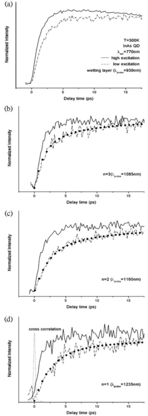
The temporal rise of the luminescence of the low QD density sample measured at the GaAs barrier’s band edge at low and high excitation intensity is shown in figure4. At both low and high excitation intensity, the PL transients show fast rise times of less than 2 ps which indicates that luminescence is dominated by the carrier relaxation within the barrier. Carriers initially excited in the barrier were then subsequently captured into the wetting layer and QDs. In figure5we also show PL transients of the wetting layer and QD confined states for the first 20 ps at room temperature. Time-resolved PL transients measured at the same energy but at two different excitation levels (low and high) are displayed together for comparison. The PL rise times of the wetting layer and excited states in the QDs decrease as the excitation power increases and reach
Carrier capture and relaxation in InAs quantum dots
Figure 4. Temporal evolution of the photoluminescence intensity
measured at the energy of the GaAs barrier under (a) high excitation (8× 10¹¹electron–hole pairs cm−2) and (b) low excitation (1× 10¹⁰electron–hole pairs cm−2) levels at room temperature.
a value of less than 2 ps at a photoexcited carrier density of
∼8 × 10¹¹ electron–hole pair cm−2. It is believed that the
carrier density dependence of the ultrafast relaxation is due to Auger-like carrier–carrier scattering [1,12]. However, in contrast to earlier reports in [12], we did not observe the PL intensity building up sequentially from the lower states at any given excitation density in our investigations. The PL rise time depends on the rates of scattering in from the upper states, and scattering out to lower levels. Therefore, our observation indicates that the intra-dot relaxation is indeed very slow, and slower than direct carrier capture. Recent studies [16–18] have shown that, due to the discrete nature of the confined states, electrons and phonons in InAs QDs are not in the weak-coupling regime but are strongly coupled to form polarons. Experimental results of intraband relaxation via polaron decay in InAs QDs were reported over a wide energy range from 40 to
∼60 meV in a more recent study [19]. Their measured energy-dependent decay time of the transmission change ranged from
∼65 to ∼45 ps and was indeed much slower than the carrier
capture time measured in our experiments.
When the excitation density is decreased to one electron– hole pair per dot, not only have the measured rise times
Figure 5. Temporal evolution of the QD luminescence intensity
measured at energies of wetting layer (a) and QD excited states (b)–(d) at room temperature. The cross correlation trace demonstrates the time resolution and the zero delay. The dotted curves shown in the figures are the best fits to the PL transients.
increased, but we also notice that the line shapes of the transients measured at the QD confined levels are very different from those at high excitation intensity. Taking the PL transient measured at the QD’s n= 1 excited state (λprobe= 1235 nm)
at low excitation intensity as an example, the luminescence 1533
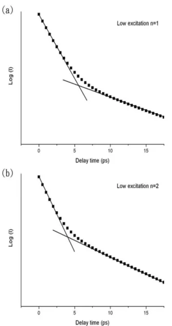
Figure 6. Differential of the best-fitted PL transient curves of the
n= 2 and 1 confined states in figures3(c) and (d).
intensity initially shows a fast rise in the first 5 ps after the photoexcitation; it is then followed by a slower increase until a maximum is reached at about 20 ps. The measured PL transients cannot be fitted by curves with only a single rise time constant. On the contrary, under high excitation, the PL intensity shows a fast rise and immediately reaches a maximum after approximately 5 ps.
The change of PL transient line shape observed under low excitation level can be explained as follows. When the best fitted curves (the dotted curves shown in figure5) of the n = 1 and 2 PL transients are differentiated and plotted on a logarithmic scale, as shown in figure6, it is clear that there are linear regions representing two different rising processes. The fast components in the PL transients give a rise time of less than 4 ps. This fast rising process is attributed to the relaxation of carriers captured directly from the GaAs barrier into the QDs’ confined state. On the other hand, the slow components shown in figure5reveal rise times which are longer than 12 ps. Keep in
Figure 7. Temporal evolution of luminescence intensity of high QD
density sample measured at energies of excited state n= 2 (a) and ground state n= 1 (b) at room temperature.
mind that, at low excitation densities, the photoexcited carriers near the dots cannot fill all the QD states; carriers excited in the barrier far away from the QD region must diffuse to the dots before they can be captured. Because holes are less mobile than electrons, the diffusion of holes becomes more important for observing the photoluminescence. For carriers with diffusion coefficient of∼10 cm2s−1, it takes approximately 10 ps for carriers to diffuse a distance of 100 nm, which is the average distance between quantum dots on the low dot density sample. This value fits well with the experimentally estimated rise time of the slow component. Carrier diffusion has also been demonstrated to have a first-order effect on the shape of time-resolved luminescence on a timescale of picoseconds in [20]. Therefore, a longer PL rise time might be observed for above barrier excitation at low densities and the capture rate is now limited by the diffusion process.
However, under high excitation, the electronic states in the QDs are quickly populated by carriers initially scattered from
Carrier capture and relaxation in InAs quantum dots
the GaAs barrier and there are enough carriers to fill the QD states. Therefore, carrier diffusion is not important and the PL rise time is now dominated by carrier capture. Further supporting evidence for our arguments is that, even at an excitation level of less than one electron–hole pair per dot, we did not observe any slow rising component in the time-resolved PL intensity (as shown in figure7) of the high density QD sample. This is because the mean separation between QDs is less than 40 nm in samples with dot density of∼1×1011cm−2.
The excited carriers in the barrier are all near the dots and the diffusion again plays a less important role as in the case of high excitation intensity.
In conclusion, we have observed the GaAs barrier, wetting layer and excited state PL transients in InAs/GaAs self-assembled QD samples of different dot densities at several excitation levels. The up-conversion technique was used to measure the rise time of the GaAs barrier, wetting layer and excited-state emission down to the photon energy of∼1 eV at room temperature. The rate of carrier transfer into the wetting layer and QDs increases with increased photoexcited carrier density. We observe fast capture and relaxation processes of the order of 1011s−1even in the one-electron–hole-pair-per-dot
regime. The line shape of the PL transients reveals a different carrier capture behaviour at low and high excitation densities. Our results suggest that, under low excitation intensity, the PL rise times are influenced by carrier diffusion. However, at high excitation density, carriers directly captured from the barrier quickly populate the QD states and fill all the states in the dots.
Acknowledgment
This work was supported by the National Science Council of the Republic of China under contract No NSC 92-2120-E-259-001.
References
[1] Bockelmann U and Egeler T 1992 Phys. Rev. B 46 15574 [2] Uskov A V, Mclnerney J, Adler F, Schweizer H and
Pilkuhn M H 1998 Appl. Phys. Lett. 72 58
[3] Ferreira R and Bastard G 1999 Appl. Phys. Lett. 74 2818 [4] Nielsen T R, Gartner P and Jahnke F 2004 Phys. Rev. B 69
235314
[5] Sosnowski T S, Norris T B, Jiang H, Singh J, Kamath K and Bhattacharya P 1998 Phys. Rev. B 57 R9423
[6] Li Q, Xu Z Y and Ge W K 2000 Solid State Commun. 115 105 [7] Sanguinetti S, Watanabe K, Tateno T, Koguchi N, Kuroda T,
Minami F and Gurioli M 2002 Appl. Phys. Lett. 81 613 [8] Tomm J W, Elsaesser T, Mazur Yu I, Kissel H, Tarasov G G,
Zhuchenko Z Ya and Masselink W T 2003 Phys. Rev. B 67 045326
[9] Dneprovskii V S, Zhukov E A, Shaygina O A, Evtikhiev V P and Kochereshko V P 2004 J. Exp. Theor. Phys. 98 156 [10] Marcinkevicius S and Leon R 2000 Appl. Phys. Lett. 76 2406 [11] Ohnesorge B, Albrecht M, Oshinowo J and Forchel A 1996
Phys. Rev. B 54 11532
[12] Yuan Z L, Foo E R A D, Ryan J F, Mowbray D J, Skolnick M S and Hopkinson M 1999 Physica B 272 12
[13] Yuan Z L, Foo E R A D, Ryan J F, Mowbray D J, Skolnick M S and Hopkinson M 2001 Phys. Status Solidi b 224 409 [14] Chu L, Arzberger A, B¨ohm G and Abstreiter G 1999 J. Appl.
Phys. 85 2355
[15] Bastard G 1988 Wave Mechanics Applied to Semiconductor Heterostructures (New York: Halsted)
[16] Hameau S, Guldner Y, Verzelen O, Ferreira R, Bastard G, Zeman J, Lemaitre A and Gerard J M 1999 Phys. Rev. Lett.
83 4152
[17] Hameau S, Isaia J N, Guldner Y, Deleporte E, Verzelen O, Ferreira R, Bastard G, Zeman J and Gerard J M 2002 Phys. Rev. B 83 085316
[18] Verzelen O, Ferreira R and Bastard G 2000 Phys. Rev. B 62 R4809
[19] Zibik E A et al 2004 Phys. Rev. B 70 161305(R)
[20] Bailey D W and Stanton C J 1992 Appl. Phys. Lett. 60 880