Cerium oxide nanocrystals for nonvolatile memory applications
Shao-Ming Yang, Chao-Hsin Chien, Jiun-Jia Huang, Tan-Fu Lei, Ming-Jinn Tsai, and Lurng-Shehng Lee
Citation: Applied Physics Letters 91, 262104 (2007); doi: 10.1063/1.2821367
View online: http://dx.doi.org/10.1063/1.2821367
View Table of Contents: http://scitation.aip.org/content/aip/journal/apl/91/26?ver=pdfcov Published by the AIP Publishing
Articles you may be interested in
Two-bit effect of trigate nanowires polycrystalline silicon thin-film-transistor nonvolatile memory with oxide/nitride/oxide gate dielectrics
Appl. Phys. Lett. 92, 163506 (2008); 10.1063/1.2910460
Ge nanocrystals in lanthanide-based Lu 2 O 3 high- k dielectric for nonvolatile memory applications J. Appl. Phys. 102, 094307 (2007); 10.1063/1.2803883
Self-assembled tungsten nanocrystals in high- k dielectric for nonvolatile memory application J. Vac. Sci. Technol. B 23, 2278 (2005); 10.1116/1.2083930
Highly thermally stable TiN nanocrystals as charge trapping sites for nonvolatile memory device applications Appl. Phys. Lett. 86, 123110 (2005); 10.1063/1.1890481
High-pressure deuterium annealing for improving the reliability characteristics of silicon–oxide–nitride–oxide–silicon nonvolatile memory devices
Appl. Phys. Lett. 85, 6415 (2004); 10.1063/1.1842363
This article is copyrighted as indicated in the article. Reuse of AIP content is subject to the terms at: http://scitation.aip.org/termsconditions. Downloaded to IP: 140.113.38.11 On: Thu, 01 May 2014 00:00:55
Cerium oxide nanocrystals for nonvolatile memory applications
Shao-Ming Yang,a兲Chao-Hsin Chien, Jiun-Jia Huang, and Tan-Fu Lei
Department of Electronics Engineering and Institute of Electronics, National Chiao-Tung University, Hsinchu, Taiwan 300, Republic of China
Ming-Jinn Tsai and Lurng-Shehng Lee
Electronics and Optoelectronics Research Laboratories, Industrial Technology Research Institute, Hsinchu, Taiwan 310, Republic of China
共Received 25 July 2007; accepted 14 November 2007; published online 27 December 2007兲 The characteristics of silicon-oxide-nitride-oxide-silicon-type memories embedded with cerium oxide nanocrystals were demonstrated. They were fabricated by depositing a thin CeO2film on the
SiO2 tunneling layer and subsequently rapid-thermal annealing process. The mean size and aerial
density of the CeO2 nanocrystals embedded in SiO2 are estimated to be about 8 – 10 nm and
共3–7兲⫻1011/cm−2 after a high-temperature annealing with different ambients on 900 ° C. The
program/erase behaviors and data retention characteristics were described to demonstrate its advantages for nonvolatile memory device applications. © 2007 American Institute of Physics. 关DOI:10.1063/1.2821367兴
In recent years, cerium dioxide共CeO2兲, which has been
extensively researched on as the buffer layer for YBa2Cu3O共7−x兲共YBCO兲 on sapphire,1an electrolyte material
of solid oxide fuel cells,2,3 buried insulator for silicon-on-insulator,4and PbZrTiCeO3ceramics,5is used for gate dielectric materials lately,6etc. Many superior properties such as lattice nearly matched to silicon共a=0.5411 nm兲 and sufficiently high dielectric constant共⬃26兲 共Refs.7and8兲 for cerium dioxide led to the high thermal stability on silicon and high scaling capacity. Silicon and metal nanocrystals 共NCs兲 are widely studied as potential solutions to overcome the scaling limitations of the conventional flash memories for future nonvolatile, high density, and low power memory devices.9–13 Recently, high- dielectric NCs on the SiO2 tunneling layer for silicon-oxide-nitride-oxide-silicon 共SONOS兲-type memories have been proposed. Lin et al.14
have reported a method of cosputtering Hf and Si in oxygen followed with high-temperature annealing to form the high- NCs for SONOS-type memory devices. However, the HfO2 nanocrystal memory exhibits saturation windows in channel-hot-electron共CHE兲 program mode. You et al.15,16have pro-posed the sol-gel spin-coating method to form the high- NCs. This method may increase thickness of tunnel oxide and results in high operation voltage.
In this study, the CeO2NCs were produced by a thermal annealing in different ambients. SONOS-type memories were fabricated and the electrical properties were investi-gated. The CeO2NC memory devices have shown good elec-trical properties in terms of large memory window共⬎2 V兲 at P/E speed of 10/10s and a retention time up to 104s with
only 10% charge loss. Our results suggest that the CeO2NC formation technique is simple and reliable, which shows a good potential for the application of the future fast nonvola-tile memories.17–19
P-type Si 共100兲 substrates with a resistivity of 5 – 10⍀ cm were used. A thin CeO2layer was deposited on SiO2 tunneling layer by an electron-beam evaporator at
10−6Torr. The samples subsequently underwent
rapid-thermal annealing共RTA兲 at 900 °C for 1 min in either O2or
N2ambient to form self-assemble CeO2 NCs. Afterward, all
samples were deposited with a 24-nm-thick blocking oxide layer by using a low-pressure tetraethoxysilane system at 700 ° C. A 200-nm-thick polycrystalline silicon 共poly-Si兲 gate was deposited and patterned. The poly-Si gate and source/drain regions were implanted with arsenic 共5 ⫻1015/cm2, 20 keV兲, and the subsequent dopant activation
annealing was performed at 950 ° C for 15 s. Finally, the CeO2 NC memory devices were completed after the
sub-strate contact patterning and metallization. The electrical properties of such devices were measured using HP 4156B semiconductor parameter analyzer and HP 41501A pulse generator.
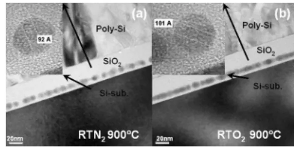
The cross-sectional transmission electron microscopy 共TEM兲 images of the CeO2 NCs embedded in the SiO2
di-electric matrix for rapid-thermal N2共RTN2兲 and O2共RTO2兲
samples are shown in Figs.1共a兲and 1共b兲, respectively. No obvious difference in microstructure in terms of NC size and disturbution are formed between annealed samples. They showed a NC density of共3–7兲⫻1011/cm2. The average NC size was 8 – 10 nm. Crystallized NCs with obviously visible lattice fringes were evident in the insets. Figure2 shows the ideal energy band diagrams of the CeO2 NC memory de-vices. The charges may be trapped in electron and hole traps in the CeO2 NCs or by charge confinement in the quantum
a兲Electronic mail: [email protected].
FIG. 1. Cross-sectional TEM images of the CeO2nanocrystals embedded in
SiO2dielectric matrix:共a兲 with RTN2annealing at 900 ° C for 1 min;共b兲
with RTO2annealing at 900 ° C for 1 min, where the average nanocrystal
size was 8 – 10 nm and obviously visible lattice fringes indicated crystalli-zation of nanocrystals.
APPLIED PHYSICS LETTERS 91, 262104共2007兲
0003-6951/2007/91共26兲/262104/3/$23.00 91, 262104-1 © 2007 American Institute of Physics This article is copyrighted as indicated in the article. Reuse of AIP content is subject to the terms at: http://scitation.aip.org/termsconditions. Downloaded to IP:
well.17 Zhang et al.20 have reported that the CeO2 band gap
is 3.15 eV and Engstrőm et al.21have indicated that the con-duction band offset between cerium oxide and silicon is 2.7 eV. The quantum well formed by the conduction band is deeper for CeO2NC structure than SONOS structure共2.7 eV compared to 1.05 eV兲.22
The programming speed of the CeO2 NCs memory
de-vices with RTN2and RTO2annealing are shown in Fig.3共a兲.
The device is programed by CHE injection. When the pro-gram voltage increases to 10 V, the Vth shift increases
rap-idly and a memory window greater than 5 V was achieved within 1 ms. The large memory windows make the multi-level operation possible. The fact the programming speed is independent of annealing condition of the charge trapping centers, indicating that the programming speed is primarily dependent on the tunneling oxide. Figure 3共b兲 shows the erasing speeds at different voltages with a fixed Vdof 10 V.
The device is erased band-to-band hot-hole 共BBHH兲 injec-tion. For the erasing speed operation, the device was pro-gramed under Vg= 10 V, Vd= 9 V with a duration of 0.1 ms.
As observed, an increase in the negative gate bias resulted in a high erasing speed due to a higher electrical field for the BBHH injection. A fully erased state was fulfilled within 1 ms when operating two samples at Vg= −7 V and
Vd= 10 V. We concluded that using the CHE for
program-ming and the BBHH for erasing has achieved high P/E ef-ficiency in the CeO2NC memory devices.
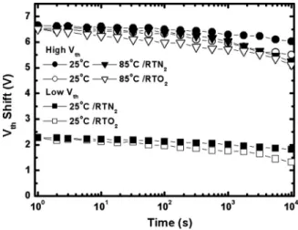
Figure 4 shows the data retention characteristics of the CeO2NC memory devices with different RTA treatments and
programming states. The RTN2 sample showed a smaller amount of charge loss at room temperature for a retention times up to 104s than the RTO2 sample. It is conjectured
that the bulk traps of RTN2 sample are deeper than RTO2
sample so that the charge loss of RTN2 sample is less than
RTO2sample. This phenomenon can be ascribed to the fact that sufficiently deep trap energy levels exist in the CeO2
NCs. At high temperature 共85 °C兲, RTN2 sample increased
charge loss rapidly after 103s. The result is because the charge loss of RTN2 sample comes from the charge in the
bulk traps. The electrons can be either trapped in these bulk defects or stay in the conduction band of the CeO2 NCs and/or in the interface states between the CeO2 NCs and
SiO2.17,22
We have demonstrated higher P/E speed of 10/10s with CeO2 NC memory devices. The RTN CeO2 NC trap-ping layers have a larger charge storage capacity and a longer retention time up to 104s with only 10% charge loss than the RTO sample due to deeper trap center. It is con-cluded that CeO2 NCs can be used as discrete charge
trap-ping sites for the SONOS-type memories.
The authors would like to thank the National Science Council of the Republic of China, Taiwan, for financially FIG. 2. Ideal energy band diagram for CeO2 nanocrystal SONOS-type
structures.
FIG. 3. 共a兲 Programming speed characteristics of CeO2 nanocrystal flash
memory devices with different programming conditions as a function of time.共b兲 The erasing speed characteristics of the CeO2nanocrystal memory
cell at different erasing voltages.
FIG. 4. Retention characteristics of CeO2nanocrystal flash memory devices
with different RTA treatments and programming states.
262104-2 Yang et al. Appl. Phys. Lett. 91, 262104共2007兲
This article is copyrighted as indicated in the article. Reuse of AIP content is subject to the terms at: http://scitation.aip.org/termsconditions. Downloaded to IP: 140.113.38.11 On: Thu, 01 May 2014 00:00:55
supporting this research under Contract No. NSC94-2215-E-009-064. The National Nano Device Laboratory, ROC, and Electronic and Optoelectronic Research Laboratories of In-dustrial Technology Research Institute are also appreciated for their technical assistance.
1F. Wang, and R. Wordenweber, Thin Solid Films 227, 200共1993兲. 2B. C. H. Steele, Solid State Ionics 12, 391共1984兲.
3M. Mogensen, N. M. Sammes, and G. A. Tompsett, Solid State Ionics
129, 63共2000兲.
4C. A. Copetti, H. Soltner, J. Schubert, W. Zander, O. Hollricher, Ch.
Buchal, H. Schulz, N. Tellman, and N. Klein, Appl. Phys. Lett. 63, 1429 共1993兲.
5J.-H. Yoo, Y.-W. Lee, S.-M. Hwang, H.-S. Yoon, H.-S. Jeong, J.-S. Kim,
and C.-S. Yoo, Proceedings of the ISAF Symposium, 2001共unpublished兲, Vol. 1, p. 495.
6L. Tye, N. A. El-Masry, T. Chikyow, P. McLarty, and S. M. Bedair, Appl.
Phys. Lett. 65, 3081共1994兲.
7N. V. Skorodumova, R. Ahuja, S. I. Simak, I. A. Abrikosov, B. Johansson,
and B. I. Lundqvist, Phys. Rev. B 64, 115108共2001兲.
8L. Kim, J. Kim, D. Jung, and Y. Roh, Appl. Phys. Lett. 76, 1881共2000兲. 9K. I. Han, Y. M. Park, S. Kim, S. H. Choi, K. J. Kim, I. H. Park, and B. G.
Park, IEEE Trans. Electron Devices 54, 359共2007兲.
10T. H. Hou, C. Lee, V. Narayanan, U. Ganguly, and E. C. Kan, 64th Device
Research Conference, 2006共unpublished兲.
11J. J. Lee, X. Wang, W. Bai, N. Lu, J. Liu, and D. L. Kwong, VLSI Tech.
Dig. 2003, 34.
12Z. Liu, C. Lee, V. Narayanan, G. Pei, and E. C. Kan, IEEE Trans. Electron
Devices 49, 1614共2002兲.
13T. H. Hou, V. Narayanan, U. Ganguly, and E. C. Kan, IEEE Trans.
Elec-tron Devices 53, 3059共2006兲.
14Y. H. Lin, C. H. Chien, C. T. Lin, C. Y. Chang, and T. F. Lei, IEEE Trans.
Electron Devices 53, 782共2006兲.
15H. C. You, F. H. Ko, and T. F. Lei, J. Electrochem. Soc. 153, F94共2006兲. 16H. C. You, T. H. Hsu, F. H. Ko, J. W. Huang, W. L. Yang, and T. F. Lei,
IEEE Electron Device Lett. 27, 653共2006兲.
17J. H. Chen, Y. Q. Wang, W. J. Yoo, Y.-C. Yeo G. Samudra, D. S. H. Chan,
A. Y. Du, and D.-L. Kwong, Tech. Dig. - Int. Electron Devices Meet. 51, 1840共2004兲.
18W. J. Tsai, N. K. Zous, C. J. Liu, C. H. Chen, T. Wang, S. Pan, and C. Y.
Lu, Tech. Dig. - Int. Electron Devices Meet. 2001, 719.
19W. J. Tsai, C. C. Yeh, N. K. Zous, C. C. Liu, S. K. Cho, T. Wang, S. C.
Pan, and C. Y. Lu, IEEE Trans. Electron Devices 51, 443共2004兲.
20F. Zhang, S.-W. Chan, J. E. Spanier, E. Apak, Q. Jin, R. D. Robinson, and
I. P. Herman, Appl. Phys. Lett. 80, 127共2002兲.
21O. Engstrőm, B. Raeissi, S. Hall, O. Buiu, M. C. Lemme, H. D. B.
Gottlob, P. K. Hurley, and K. Cherkaoui, Solid-State Electron. 51, 662 共2007兲.
22Y.-N. Tan, W.-K. Chim, B. J. Cho, and W.-K. Choi, IEEE Trans. Electron
Devices 51, 1143共2004兲.
262104-3 Yang et al. Appl. Phys. Lett. 91, 262104共2007兲
This article is copyrighted as indicated in the article. Reuse of AIP content is subject to the terms at: http://scitation.aip.org/termsconditions. Downloaded to IP: 140.113.38.11 On: Thu, 01 May 2014 00:00:55