亞東技術學院
資訊與通訊工程研究所
碩士論文
應用於 WIFI 之高效率套筒偶極天線設計
High Efficiency Sleeve Dipole Antenna
Design for WIFI
研 究 生:陳俊傑
指導教授:張道治
誌謝
完成論文之後,也代表即將進入人生新的階段,在研究所這
段期間學習到非常多的東西,除了學業上的知識之外,還有許
多做事情的方法、與同學間相處的方法,這些事情都是相當重
要的。
非常感謝我的指導教授張道治教授,在這段期間教導我非常
多的知識,以及帶領我參加非常多的國際研討會,參加產學計
畫案的合作等...讓我的眼界寬廣了許多。感謝從大學到研究所一
直互相扶持的好朋友紹翔、笛翰、晟瑋,以及研究所的學長廖
兆祥、學弟學妹們,實驗室中心助理千慧、裕中,這段時間承
蒙照顧了,因為有你們我才能度過這段期間,很高興認識你們,
希望你們的未來可以更順利更快樂。
最後感謝我的家人,我親愛的老爸,雖然說話的機會不多,
但是我知道你一直很支持我,也一直在等,快了快了!!!
中文摘要
近年來無線通訊技術越來越發達,已經被廣泛的應用在企業或是個 人通訊上並且正在積極的推動所有可能性,目前在日常生活中最常見的 就是 WiFi(Wireless fidelity),WiFi 是一個無線網路通訊技術的品牌,被廣 泛的應用在各大城市中。 因此在本篇論文中,將設計應用於無線通訊網路 WiFi IEEE 802.11 a/b/g 所使用的天線來做探討,工作頻率分別是 2.45 GHz 以及 5.8 GHz, 論文中將分為兩大部分做介紹分別是立體式的套筒陣列天線為主,及平 面式的套筒陣列天線為主,由於都是串聯式的陣列天線,所以在論文中 將研究如何降低串聯式陣列天線的損耗功率以提升天線的效率,讓串聯 式的陣列天線可以發揮出更高的天線增益。 另外在論文中,有設計一應用在 HSPDA 的平面倒 F 天線,HSDPA 是 High Speed Downlink Packet Access 的縮寫,是一種行動通訊協議,亦 稱為 3.5G,HSPDA 應用的頻段較多,分別為 850 MHz、1900 MHz 以及 2100 MHz,然而在通訊系統上空間相當重要,因此設計平面倒 F 天線來 達到多頻帶以及體積小的要求。 關鍵字:WIFI、套筒偶極天線陣列、IEEE 802.11 a/b/g、HSDPA、平面倒 F 天線Abstract
The past decade has seen a phenomenal growth in wireless communications. Wireless technology is permeating business and personal communications are across the globe, and the demand is driving the availability and performance to the new levels. WiFi(Wireless Fidelity) is the most common communication standard.
In this research, which design coaxial sleeve dipole antenna array and the sleeve dipole antenna array by print circuit board for IEEE 802.11a/b/g, which operate frequencies are 2.45 GHz and 5.8 GHz. and the sleeve dipole antenna array by print circuit board can combine reflector to increase directivity. The sleeve dipole antenna array by print circuit board is linear antenna array , when antenna elements more and more, the taper efficiency is very important, so this thesis, will optimize of taper efficiency to get best directivity. The simulations are done by using GEMS, a parallelized FDTD (Finite-Difference Time-Domain) code
In this thesis, the planar inverted F antenna is designed for HSDPA. High-Speed Downlink Packet Access (HSDPA) is an enhanced 3G (third generation) mobile telephony communications protocol in the High-Speed Packet Access (HSPA) family, also called 3.5 G, which the operate frequencies are 850 MHz, 1900 MHz and 2100 MHz, however, the space is very important in communication system, so the planar inverted-F antenna
will be designed to achieve multi-band and small size requirements.
Key Words:WiFi、 sleeve dipole antenna array 、IEEE 802.11a/b/g、 linear antenna array 、HSDPA、inverted F antenna by print circuit board
Contents
博碩士論文授權書...I 論文封面...II 論文指導教授薦書...III 論文口試委員審定書...IV 誌謝...V Chinese Abstract...VI English Abstract...VII Contents...IX List of Table...XI List of Figures...XIIChapter 1 Introduction...1
1.1 Research Motivation...1 1.2 Introduction of WIFI...2 1.3 Introduction of 802.11a/b/g...2 1.4 Thesis Outlines...3Chapter 2 Design of Coaxial Sleeve Dipole Antenna...5
2.1 Theory of Sleeve Dipole Antenna...5
2.2 Simulation of Coaxial Sleeve Dipole Antenna...6
2.3 Simulation and Measurement Results of Sleeve Dipole Antenna...7
2.4 Summary...8
Chapter 3 Design of Coaxial Sleeve Dipole Antenna Array...15
3.1 Motivation...15
3.2 Theory of Antenna Array...15
3.3 Simulation of Coaxial Sleeve Dipole Antenna Array...18
3.4 Simulation and Measurement Results of Sleeve Dipole Antenna Array...19
Chapter 4 Sleeve Dipole Antenna Array by Print Circuit
Board...26
4.1 Introduction of Sleeve Dipole Antenna Array by Print Circuit Board...26
4.2 Simulation of Sleeve Dipole Antenna Array by Print Circuit Board...27
4.3 Simulation and Measurement Results of Sleeve Dipole Antenna Array by Print Circuit Board...30
4.4 Summary...32
Chapter 5 Design of Planar Inverted F Antenna For HSDPA.50
5.1 Introduction of HSDPA...505.2 Introduction of Planar Inverted F Antenna...52
5.3 Simulation of Planar Inverted F Antenna...53
5.4 Simulation and Measurement Results of Planar Inverted F Antenna..54
5.5 Summary...55
Chapter 6 Conclusion...67
6.1 Summary...67
List of Table
List of Figures
Fig 2.1 Structure of dipole antenna………...………9
Fig 2.2 Structure of sleeve antenna………...9
Fig 2.3 Structure of sleeve Balun………...10
Fig. 2.4 Structure of coaxial sleeve dipole antenna………...10
Fig. 2.5 Fabricated of the coaxial sleeve dipole antenna………...11
Fig. 2.6 Simulation and measurement result of reflection coefficient...12
Fig. 2.7 Measurement environment of coaxial sleeve dipole antenna...12
Fig. 2.8 Simulation and measurement results of efficiency…………...13
Fig. 2.9 Simulation and measurement results of peak gain…………...13
Fig. 2.10 Simulation and measurement results of E-plane radiation pattern at 2.45GHz…...………14
Fig. 2.11 Simulation and measurement results of H-plane radiation pattern at 2.45GHz………...14
Fig. 3.1 Structure of Antenna Array…...…...…...………...21
Fig. 3.2 Equivalent circuit of traveling-wave linear array………...21
Fig. 3.3 Structure of coaxial sleeve dipole antenna array …………...22
Fig. 3.4 Fabricated of the coaxial sleeve dipole antenna array ……...22
Fig. 3.5 Measurement environment of coaxial sleeve dipole antenna array ………..23
Fig. 3.6 Simulation and measurement result of reflection coefficient...23
Fig. 3.7 Simulation and measurement result of efficiency………...…...24
Fig. 3.8 Simulation and measurement result of peak gain…...24
Fig. 3.9 Simulation and measurement result of E-plane radiation pattern at 2.45 GHz...25
Fig. 3.10 Simulation and measurement result of H-plane radiation pattern at 2.45 GHz...25
Fig. 4.1 WiFi apply in town...33
Fig. 4.2 Simulation model of sleeve dipole antenna array for IEEE 802.11b/g...33
Fig. 4.3 Simulation model of sleeve dipole antenna array for IEEE 802.11a...34
Fig. 4.4 Equivalent circuit of the sleeve dipole antenna array by print circuit board...34
Fig. 4.5 Simulation result of admittance with thickness 0.08 cm...35
Fig. 4.7 Simulation models of sleeve dipole antenna array by print circuit
board...36
Fig. 4.8 The simulation results of the reflection coefficient...36
Fig. 4.9 Simulation results of efficiency...37
Fig. 4.10 Simulation results of directivity...37
Fig. 4.11 Simulation results of the peak gain...38
Fig. 4.12 Fabricated of the sleeve dipole antenna array by print circuit board...38
Fig. 4.13 The measurement environment...39
Fig. 4.14 Simulation and measurement result of the reflection coefficient...39
Fig. 4.15 Simulation and measurement result of efficiency...40
Fig. 4.16 Simulation and measurement result of the peak gain...40
Fig. 4.17 Simulation and measurement result of E-plane pattern at 2.41 GHz...41
Fig. 4.18 Simulation and measurement result of H-plane pattern at 2.41 GHz...41
Fig. 4.19 Simulation and measurement result of E-plane pattern at 2.44...42
Fig. 4.20 Simulation and measurement result of H-plane pattern at 2.44 GHz...42
Fig. 4.21 Simulation and measurement result of E-plane pattern at 2.46 GHz...43
Fig. 4.22 Simulation and measurement result of H-plane pattern at 2.46 GHz...43
Fig. 4.23 Fabricated sleeve dipole antenna array by print circuit board...44
Fig. 4.24 Measurement environment of sleeve dipole antenna array by print circuit board...44
Fig. 4.25 Simulation and measurement result of the reflection coefficient...45
Fig. 4.26 Simulation and measurement result of efficiency...45
Fig. 4.27 Simulation and measurement result of peak gain...46
Fig. 4.28 Simulation and measurement result of E-plane pattern at 5.2 GHz...46
Fig. 4.29 Simulation and measurement result of H-plane pattern at 5.2 GHz...47 Fig. 4.30 Simulation and measurement result of E-plane pattern at 5.5
GHz...47
Fig. 4.31 Simulation and measurement result of H-plane pattern at 5.5 GHz...48
Fig. 4.32 Simulation and measurement result of E-plane pattern at 5.8 GHz...48
Fig. 4.33 Simulation and measurement result of H-plane pattern at 5.8 GHz...49
Fig. 5.1 Structure of the monopole antenna and the inverted L antenna...56
Fig. 5.2 Structure of planar inverted F antenna...56
Fig. 5.3 Simulated model of the planar inverted F antenna A...57
Fig. 5.4 Simulated model of the planar inverted F antenna B...57
Fig. 5.5 Simulation results of the return loss...58
Fig. 5.6 Fabricated of the planar inverted F antenna B...58
Fig. 5.7 Measurement environment...59
Fig. 5.8 Simulation and measurement result of the return loss...59
Fig. 5.9 Simulation and measurement result of efficiency at low band...60
Fig. 5.10 Simulation and measurement result of efficiency at high band...60
Fig. 5.11 Simulation and measurement result of peak gain at low band...61
Fig. 5.12 Simulation and measurement result of peak gain at high band...61
Fig. 5.13 Simulation and measurement result of 2D pattern in phi 0 deg at 850 MHz...62
Fig. 5.14 Simulation and measurement result of 2D pattern in phi 90 deg at 850 MHz...62
Fig. 5.15 Simulation and measurement result of 2D pattern in theta 90 deg at 850 MHz...63
Fig. 5.16 Simulation and measurement result of 2D pattern in phi 0 deg at 1900 MHz...63
Fig. 5.17 Simulation and measurement result of 2D pattern in phi 90 deg at 1900 MHz...64
Fig 5.18 The simulation and measurement result of 2D pattern in theta 90 deg at 1900 MHz...64
Fig. 5.19 Simulation and measurement result of 2D pattern in phi 0 deg at 2100 MHz...65
Fig. 5.20 Simulation and measurement result of 2D pattern in phi 90 deg at 2100 MHz...65 Fig. 5.21 Simulation and measurement result of 2D pattern in theta 90 deg at
Chapter 1
Introduction
1.1 Research Motivation
In telecommunications, wireless communication may be used to transfer information over short distances (a few meters as in television remote control) or long distances (thousands or millions of kilometers for radio communications). The term is often shortened to "wireless". The past decade has seen a phenomenal growth in wireless communications. Wireless technology is permeating business and personal communications are across the globe, and the demand is driving the availability and performance to the new levels. The wireless communication is widely applied in many aspects, such as military, navigation, aviation, scientific research, etc…
Wireless networking (i.e. the various types of unlicensed 2.4 GHz WiFi devices) is used to meet many needs. Perhaps the most common is used to connect laptop users who travel from location to location. Another common is used for mobile networks that connect via satellite. A wireless transmission method is a logical choice to network a LAN segment that must frequently change locations. And in the wireless local area network, WiFi is the most common communication standard
1.2 Introduction of WiFi
Wi-Fi is a wireless communication technology brand, the Wi-Fi Alliance (Wi-Fi Alliance) held, used on certified products based on IEEE 802.11 standards, the objective is to improve the standard IEEE 802.11-based wireless network Road interoperability.
1.3 Introduction of IEEE 802.11a/b/g
IEEE 802.11 is a set of standards for implementing wireless local area network (WLAN) computer communication in the 2.4, 3.6 and 5 GHz frequency bands. They are created and maintained by the IEEE LAN/MAN Standards Committee (IEEE 802). The base current version of the standard is IEEE 802.11-2007.
The IEEE 802.11a standard uses the same data link layer protocol and frame format as the original standard, but an OFDM based air interface (physical layer). It operates in the 5 GHz band with a maximum net data rate of 54 Mbit/s, plus error correction code, which yields realistic net achievable throughput in the mid-20 Mbit/s. Since the 2.4 GHz band is heavily used to the point of being crowded, using the relatively unused 5 GHz band gives IEEE 802.11a a significant advantage. However, this high carrier frequency also brings a disadvantage: the effective overall range of IEEE 802.11a is less than that of 802.11b/g. In theory, IEEE 802.11a signals are absorbed more
readily by walls and other solid objects in their path due to their smaller wavelength and, as a result, cannot penetrate as far as those of IEEE 802.11b. In practice, IEEE 802.11b typically has a higher range at low speeds (IEEE 802.11b will reduce speed to 5 Mbit/s or even 1 Mbit/s at low signal strengths). However, at higher speeds, IEEE 802.11a often has the same or greater range due to less interference.
IEEE 802.11b has a maximum raw data rate of 11 Mbit/s and uses the same media access method defined in the original standard. IEEE 802.11b products appeared on the market in early 2000, since IEEE 802.11b is a direct extension of the modulation technique defined in the original standard. The dramatic increase in throughput of IEEE 802.11b (compared to the original standard) along with simultaneous substantial price reductions led to the rapid acceptance of IEEE 802.11b as the definitive wireless LAN technology.
IEEE 802.11g is works in the 2.4 GHz band (like IEEE 802.11b), but uses the same OFDM based transmission scheme as IEEE 802.11a. It operates at a maximum physical layer bit rate of 54 Mbit/s exclusive of forward error correction codes, or about 22 Mbit/s average throughput.
1.4 Thesis Outlines
In Chapter 2, design of a sleeve dipole antenna for IEEE 802.11b/g, Introduction of basic omni-directional antenna in this chapter, and the simulated and measured results of optimized design are given as well.
In Chapter 3, design of a sleeve dipole antenna array for IEEE 802.11b/g, and the simulated and measured results of optimized design are given as well.
In Chapter 4, design of a Print sleeve dipole antenna array for IEEE 802.11a/b/g, improve taper efficiency of printed sleeve dipole antenna array in this chapter. The Print sleeve dipole antenna array is linear antenna array, when antenna elements are more and more, the taper efficiency is very important, this chapter, optimize taper efficiency to get best directivity.
In Chapter 5, design a Planar Inverted F Antenna for HSDPA, the operating frequencies are 850MHz、1900 MHz and 2100 MHz, and the simulated and measured results of optimized design are given as well.
Chapter 2
Design of Coaxial Sleeve Dipole Antenna
This chapter will discuss the omni-directional antenna. This section design the coaxial sleeve dipole antenna, however, the coaxial sleeve dipole antenna is evolved by the dipole antenna.
2.1 Theory of Sleeve Dipole Antenna
According to transmission line theory, when a transmission line is open circuit, if it add a feed in transmission line, which will form a dipole antenna, as shown in Fig 2.1, and the length of the transmission line will determine the operating frequency, when the length of the transmission line is half wavelength, would be generated the standing wave resonance to feed of the signal, and the current of dipole antenna is sinusoidal current distribution, the current distribution on the dipole antenna is given by
(2-1)
From (2-1), when the parameter Z is zero, in the center of antenna will get the largest current, and the current will equal to 0 at the antenna terminal. The radiation pattern of dipole antenna is omni-direction. The ideal gain of
|)]
|
4
(
[
I
)
(
z
MAXSin
z
I
impedance matching, because the impedance of dipole antenna is 73 + j42.5 ohms. The disadvantage is the length of dipole antenna must be half-wavelength.
2.1.1 Theory of Balun
Coaxial cable feed dipole antenna, unfortunately, the coaxial cable will produce the unbalance current, as shown in Fig. 2.2, however, the unbalance current will influence to the radiation pattern of dipole antenna, so it need to design a Balun. Balun is the abbreviations of "balance" and "Unbalance", which is used to transform the unbalanced input into balanced output and have wide range of applications.
In this research, the outer conductor connected to a quarter wavelength of the sleeve as a Balun, as shown in Fig. 2.3. The ratio of r2 over r1 will influence the length of the sleeve, when the ratio is set between 2 to 3, the length of Balun about is quarter-wavelength, if the ratio is set between 3 to 8, the length of Balun will be shorter than quarter-wavelength. The name of coaxial sleeve dipole antenna is combining of sleeve and dipole antenna.
2.2 Simulation of Coaxial Sleeve Dipole Antenna
dipole antenna designed to be applied in IEEE 802.11 b/g, and operating frequency at 2.4 GHz, the quarter-wavelength is 3 cm, from Fig 2.5, the coaxial sleeve dipole antenna is combined with the dipole antenna and Balun, as is the dipole antenna, the ideal gain of dipole antenna is 2.15 dBi. The ratio of inner conductor and teflon will influence the impedance of cable, so it need to make sure the impedance of cable is 50 ohm, A simulation model by GEMS, The structure of the coaxial sleeve dipole antenna is shown in Fig 2.5, The parameter X and the parameter Y are about quarter-wavelength of operating frequency, the parameter A is diameter of inner conductor, the parameter B is diameter of teflon, the parameter C is a distance between the Balun to the outer conductor.
The optimization result for the length of coaxial sleeve dipole antenna are shown in table 1, when the parameter X is equal to 2.8 cm, the simulation result of S11 is -14.5 dB, the simulation result of efficiency is 93%, the simulation result of peak gain is 1.88 dBi, so when the parameter X is equal to 2.8 cm, which can get best result.
2.3 Simulation and Measurement Results of Sleeve Dipole
Antenna
The fabricated of the coaxial sleeve dipole antenna is shown in Fig. 2.5, the simulation and measurement results of the reflection coefficient are shown in Fig. 2.6, the whole bandwidth covers the operating frequency. The
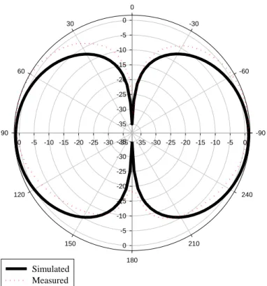
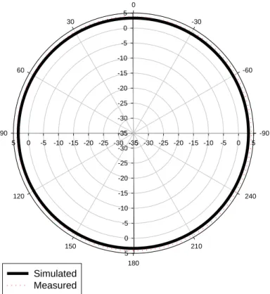
measurement environment of coaxial sleeve dipole antenna is shown in Fig. 2.7. The measurement system is SATIMO Star-Lab. It is a spherical Near-Field measurement system. The simulation and measurement results of efficiency are shown in Fig. 2.8. The measurement result of efficiency is about 85%. The simulation and measurement results of peak gain are shown in Fig. 2.9. The measurement result of peak gain is about 1.9 dBi. The simulation and measurement result of E-plane radiation pattern at 2.45 GHz are shown in Fig. 2.10. The simulation and measurement result are almost the same. The simulation and measurement results of H-plane radiation pattern at 2.45GHz are shown in Fig. 2.11. The radiation pattern at H-plane is almost omni-direction.
2.4 Summary
The peak gain of coaxial sleeve dipole antenna is about 1.9 dBi, the efficiency is about 85%. The radiation pattern at H-plane is almost omni-direction.
λ /2
λ /2
Fig 2.1 Structure of dipole antenna
2.75 cm 2.75 cm X Y Copper Copper A B C Teflon quarter-wavelength 2×r1 r2 Outer conductor Inner conductor Teflon quarter-wavelength 2×r1 r2 Outer conductor Inner conductor Teflon 2×r1 r2 Outer conductor Inner conductor Inner conductor Teflon Teflon
Fig 2.3 Structure of sleeve Balun
Fig. 2.4 Structure of coaxial sleeve dipole antenna Unit:mm
A 0.4 B 1.4 C 2
X Efficiency at 2.45GHz S11 at 2.45GHz Peak Gain at 2.45GHz 3 cm 80 % -9 dB 1.32 dBi 2.8 cm 93 % -14.5 dB 1.88 dBi 2.75 cm 92 % -12.5 dB 1.87 dBi 2.7 cm 91 % -11.5 dB 1.82 dBi
Table 1 Optimization for X length of coaxial sleeve dipole antenna
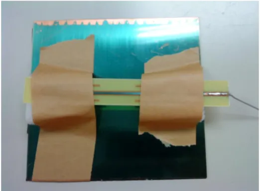
Fig. 2.5 Fabricated of the coaxial sleeve dipole antenna
1/4 wavelengt h 波長 1/4 wavelength 1/2 wavelengt h 波長 Unit:mm
Frequency (GHz) 2.0 2.1 2.2 2.3 2.4 2.5 2.6 |S 11|(dB) -20 -15 -10 -5 0 Simulated Meassured
Fig. 2.6 Simulation and measurement result of reflection coefficient
Frequency (GHz) 2.30 2.35 2.40 2.45 2.50 2.55 2.60 E ff icie nc y (% ) 0.2 0.3 0.4 0.5 0.6 0.7 0.8 0.9 1.0 Simulated Measured Frequency (GHz) 2.30 2.35 2.40 2.45 2.50 2.55 2.60 P eak Gain(dB i) -8 -6 -4 -2 0 2 4 6 Simulated Measured
Fig. 2.8 Simulation and measurement results of efficiency
-35 -30 -25 -20 -15 -10 -5 0 -35 -30 -25 -20 -15 -10 -5 0 -35 -30 -25 -20 -15 -10 -5 0 -35 -30 -25 -20 -15 -10 -5 0 -90 -60 -30 0 30 60 90 120 150 180 210 240 Simulated Measured -35 -30 -25 -20 -15 -10 -5 0 -35 -30 -25 -20 -15 -10 -5 0 -35 -30 -25 -20 -15 -10 -5 0 -35 -30 -25 -20 -15 -10 -5 0 -90 -60 -30 0 30 60 90 120 150 180 210 240 Simulated Measured
Fig. 2.10 Simulation and measurement results of E-plane radiation pattern at 2.45GHz
Fig. 2.11 Simulation and measurement results of H-plane radiation pattern at 2.45GHz
Chapter 3
Design of Coaxial Sleeve Dipole Antenna array
In chapter 2, the peak gain of the coaxial sleeve dipole antenna is about 1.9 dBi. For long distance WiFi communication, the antenna gain is very important, so in this chapter, will design sleeve dipole antenna array to increase antenna gain.
3.1 Motivation
The radiation pattern of coaxial sleeve dipole antenna is omni-direction, it can cover any direction, Unfortunate, for long distance WIFI communication, the antenna gain is very important, so in this chapter, it design sleeve dipole antenna array to increase antenna gain. The sleeve dipole antenna array has high gain, and the radiation pattern like the coaxial sleeve dipole antenna is omni-direction too.
3.2 Theory of Antenna Array
An antenna array is an antenna that is composed of more than one antenna elements, each antenna elements has the same amplitude and phase, the interval between each antenna elements is about half-wavelength.
( ) sin 1 1)
(
)
(
jk N n d N n n N jkr n jkr n N nf
a
e
r
e
r
e
f
a
E
N n
N jkr d n N jk N n n N jkr r e e a f r e E N N
( ) sin 1 ) (
sin
)
(
N
n
d
r
r
n
N
antenna array are more high directivity and peak gain.
The radiation pattern of antenna array is sum of the radiation pattern of each antenna elements, the radiation pattern of antenna array is shown in Fig 3.1. Generally, the main beam generate in the middle of the antenna array, when the antenna elements are more and more, the antenna gain is more higher, but the main beam will be narrower.
a. Theory of Array Factor
If there are N elements along x-direction with spacing d, the total field intensity with identical element pattern
(3-1)
In which an is the amplitude excitation. F(θ) is nth antenna element pattern.Then the total electric field intensity is
sin ) ( 1 d n N jk N n
e
a
AF
So Array Factor is (3-3) Exclude the phase term, the AF is a SINC function with maximum value is with half-wavelength element spacing.b. Theory of Array Admittance
The sleeve dipole antenna array is linear antenna array, when an antenna element is more and more, the taper efficiency is very important. Follow R.S.ELLIOTT paper [2] “On the Design of Traveling-Wave-Fed Longitudinal Shunt Slot Arrays”, equivalent circuit of traveling-wave linear array is shown in Fig. 3.2, Yn
A
is the admittance of antenna element, βL is the space distance, Go is match load. The equation of voltage and current can write
(3-4)
And power radiated from each antenna element is
)
log(
20
N
or
N
L
Z
jV
L
I
I
L
Z
jI
L
V
V
out out in out out in
sin
cos
sin
cos
0 0
*Re
2
1
G
Y
V
V
P
n n n n
So
(3-6)
When P1=P2=P3=….Pn, we can get the best taper efficiency, Eq. (3-5) and (3-6) combined to give
(3-7)
From (3-7), when power radiated of each antenna element are equal, sleeve dipole antenna array have the best taper efficiency. So the linear antenna array can change admittance of each antenna element to get best taper efficiency. Chapter 4, will optimize of taper efficiency to get best antenna directivity.
3.3 Simulation of Coaxial Sleeve Dipole Antenna array
The structure of the coaxial sleeve dipole antenna array is shown in Fig. 3.3, it add a helix to construct an array, which can make electric field in the same direction to increase antenna gain by shifting the phase, and parameter H is equal to half-wavelength, which is second antenna element. In the coaxial sleeve dipole antenna array, the helix is very important, the length of the helix is about half-wavelength, when the length is equal to half-wavelength, and the phase is shifting 180 degree. When the length isn't
... 0 3 * 3 3 0 2 * 2 2 0 1 * 1 1 * * * G Y V V G Y V V G Y V V A A A O n n n n total G Y V V P P * Re 2 1
equal half-wavelength, the main beam will be scan, in WiFi communication, this is very serious problem. Because the coaxial sleeve dipole antenna array is dipole antenna, so the length of each antenna elements must equal half-wavelength.
In Fig. 3.3, the defining parameters of the conventional helix are the helix radius, R ,the total length of the helix, CL ,the turn-to-turn spacing, TD ,and the axial length, Z.
3.4 Simulation and Measurement Results of Sleeve Dipole
Antenna Array
The fabricated of the coaxial sleeve dipole antenna array is shown in Fig. 3.4, the measurement environment is shown in Fig 3.5. The simulation and measurement results of the reflection coefficient are shown in Fig. 3.6, the whole bandwidth covers the operating frequency. The simulation and measurement results of efficiency are shown in Fig. 3.7, the measurement result of efficiency is about 90%. The simulation and measurement results of peak gain are shown in Fig 3.8, the measurement result of peak gain is about 4.2 dBi. The simulation and measurement result of E-plane radiation pattern at 2.45 GHz are shown in Fig 3.9, the simulation and measurement result is almost the same. The simulation and measurement result of H-plane radiation pattern at 2.45 GHz are shown in Fig 3.10, from Fig 3.10, it can find
the radiation pattern of coaxial coaxial sleeve dipole antenna is belonging to omni-direction.
3.5 Summary
The gain of the coaxial sleeve dipole antenna array is about 4.2 dBi, and the efficiency is about 90%, and the radiation pattern at H-plane is almost omni-direction.
Fig. 3.1 Structure of antenna array
Fig. 3.2 Equivalent circuit of traveling-wave linear array
Fig. 3.3 Structure of coaxial sleeve dipole antenna array
Fig. 3.4 Fabricated of the coaxial sleeve dipole antenna array
H
R
TD
Z
Unit:mm
17
X
57
H
11
Z
2.5
TD
2
R
62.8
CL
Unit:mmFrequency (GHz) 2.0 2.1 2.2 2.3 2.4 2.5 2.6 |S 11|(dB ) -20 -15 -10 -5 0 Simulated Meassured
Fig. 3.5 Measurement environment of coaxial sleeve dipole antenna array
Fig. 3.7 Simulation and measurement result of efficiency
Fig. 3.8 Simulation and measurement result of peak gain
Frequency (GHz) 2.30 2.35 2.40 2.45 2.50 2.55 2.60 Ef fi cienc y (%) 0.2 0.3 0.4 0.5 0.6 0.7 0.8 0.9 1.0 Simulated Measured Frequency (GHz) 2.30 2.35 2.40 2.45 2.50 2.55 2.60
Peak Gain (dBi)
-8 -6 -4 -2 0 2 4 6 Simulated Measured
Fig. 3.9 Simulation and measurement result of E-plane radiation pattern at 2.45 GHz
Fig. 3.10 Simulation and measurement result of H-plane radiation pattern at 2.45 GHz -35 -30 -25 -20 -15 -10 -5 0 -35 -30 -25 -20 -15 -10 -5 0 -35 -30 -25 -20 -15 -10 -5 0 -35 -30 -25 -20 -15 -10 -5 0 -90 -60 -30 0 30 60 90 120 150 180 210 240 Simulated Measured -35 -30 -25 -20 -15 -10 -5 0 5 -35 -30 -25 -20 -15 -10 -5 0 5 -35 -30 -25 -20 -15 -10 -5 0 5 -35 -30 -25 -20 -15 -10 -5 0 5 -90 -60 -30 0 30 60 90 120 150 180 210 240 Simulated Measured
Chapter 4
Sleeve Dipole Antenna array by Print Circuit Board
In Chapter 4, a sleeve dipole antenna array by print circuit board will be designed for IEEE 802.11a/b/g, and improving taper efficiency in this chapter, the sleeve dipole antenna array by print circuit board will add an reflector to change radiation pattern. The sleeve dipole antenna array is linear antenna array, when antenna elements are more and more, the taper efficiency is very important, in this chapter, we optimize of taper efficiency to get best directivity.
4.1 Introduction of Sleeve Dipole Antenna array by Print
Circuit Board
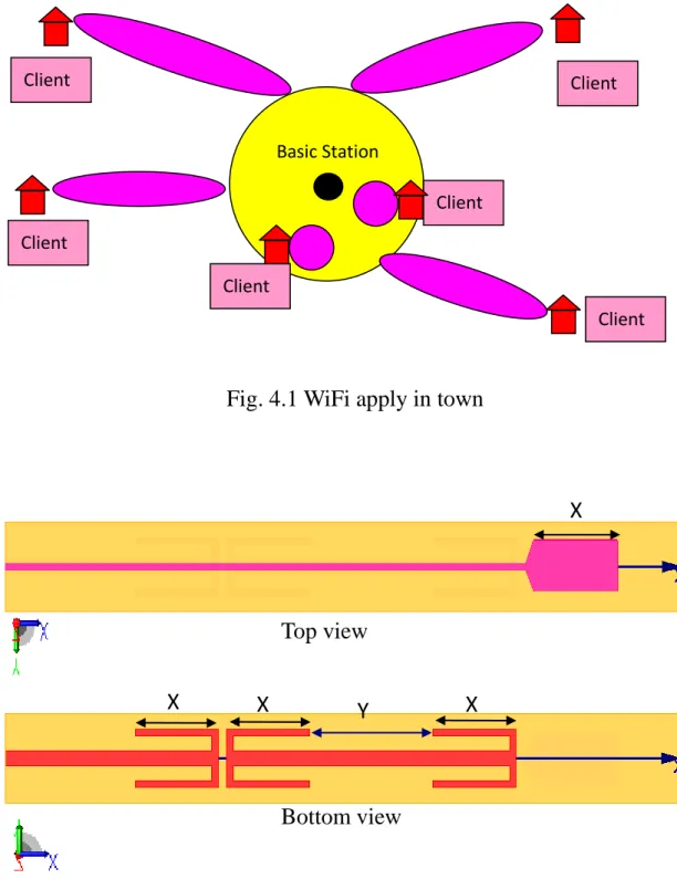
Fig 4.1 is show WiFi apply in town, the base station at town center, unfortunately, for long distance client need high antenna gain to connect base station.
In this chapter, design of the sleeve dipole antenna array by print circuit board, and add a reflector to increase antenna gain, the radiation pattern of the sleeve dipole antenna array will be change. The sleeve dipole antenna array is wideband antenna array, Unfortunately, the main beam will scan at different frequency.
4.2 Simulation of Sleeve Dipole Antenna array by Print Circuit
Board
The sleeve dipole antenna array is designed to be applied in IEEE 802.11a and IEEE 802.11b/g, operating frequency are from 2.41 GHz to 2.46 GHz and 5.2 GHz to 5.8 GHz, due to operating frequency of IEEE 802.11a is wider, so the main beam will obvious scan.
a. Simulation of Sleeve Dipole Antenna array for IEEE 802.11 b/g
Simulation model of sleeve dipole antenna array is shown in Fig. 4.2. The substrate is FR4 with thickness 0.08 cm. The size of substrate is 16 cm in length and 2.1 cm in width. The operating frequency of IEEE 802.11 b/g is from 2.41 GHz to 2.46 GHz. The parameter X is about quarter-wavelength, the parameter Y is distance of each antenna element, and the main beam can scan at different frequency. The sleeve dipole antenna array will add a reflector, which increase antenna gain is about 6 dB. The height of the sleeve dipole antenna array to the reflector is about 2 cm.
b. Simulation of Sleeve Dipole Antenna array for IEEE 802.11a
Simulation model of sleeve dipole antenna array is shown in Fig. 4.3. The substrate is FR4 with thickness 0.08 cm. The size of substrate is 12.5 cm in
3 2
1
Y
Y
Y
length and 1.3 cm in width. The operating frequency of IEEE 802.11 a is from 5.2 GHz to 5.8 GHz. The parameter X is about quarter-wavelength, the parameter Y is distance of each antenna element, and the main beam can scan at different frequency. The sleeve dipole antenna array will add a reflector, which increase antenna gain is about 6 dB. The height of the sleeve dipole antenna array to the reflector is about 0.75 cm.
c. Optimization of Antenna Admittance
When the operating frequency is higher, the wavelength is shorter, the sleeve dipole antenna array can contain more antenna element in the same size. The sleeve dipole antenna array is linear antenna array, when an antenna element is more and more, the taper efficiency is very important. From the chapter 3, which can know, when P1=P2=P3=….Pn, we can get the best taper efficiency, from Eq. 3-7, which can know the linear antenna array can change admittance of each antenna element to get best taper efficiency. Follow R.S.ELLIOTT paper “On the Design of Traveling-Wave-Fed
Longitudinal Shunt Slot Arrays” [1], the equation of voltage can write
(4-1) If βL is half-wavelength, Eq. 3-7 and Eq 4-1 combined to give
(4-2) When admittance of each antenna element is equal, the sleeve dipole
)
sin
(cos
0 1 1L
G
Y
j
L
V
V
n
n
n
antenna array has the best taper efficiency. This paper design of sleeve dipole antenna array by print circuit board, due to the print circuit board have insertion loss, the current will be weaken. The equivalent circuit of the sleeve dipole antenna array by print circuit board is shown in fig 4.4, the a1 and a2 are
admittance of insertion loss. The antenna element more and more, the antenna admittance is larger.
In Fig 4.3, the parameter D is space of feed, which can control the array admittance. Fig. 4.5 and Fig. 4.6 are show simulation result of admittance with thickness 0.08 cm and 0.04 cm, the parameter D and admittance are in direct proportion.
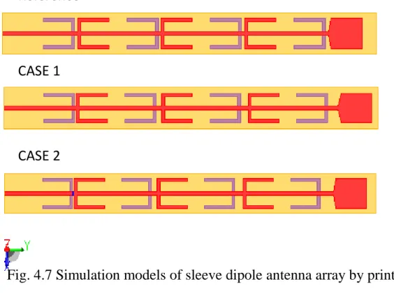
The simulation models of sleeve dipole antenna array by print circuit board are shown in Fig 4.7. The each antenna element has equal admittance is shown in Reference, optimization of the antenna admittance are shown in CASE1 and CASE 2. The simulation results of the return loss are shown in Fig 4.8. The whole bandwidth covers the operating frequency, from 5.2 GHz to 5.8 GHz. The simulation results of efficiency are shown in Fig. 4.9. The efficiency of the reference is about 60%. The efficiency of the CASE2 is about 65%. The simulation results of directivity are shown in Fig. 4.10. The directivity of the reference is about 7.5 dBi. The directivity of the CASE2 is about 8 dBi. The simulation results of peak gain are shown in Fig. 4.11. The peak gain of the reference is about 5 dBi. The peak gain of the CASE2 is about 5.5 dBi. After optimization of antenna admittance, the peak gain has been increased 0.5 dBi, the directivity has been increased 0.5dBi, and the
efficiency has been also increased.
4.3 Simulation and Measurement Results of Sleeve Dipole
Antenna array by Print Circuit Board
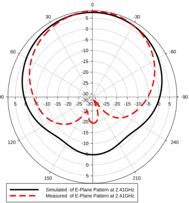
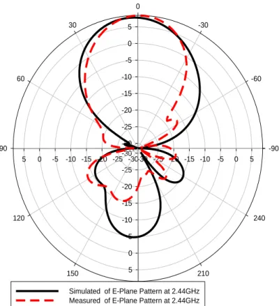
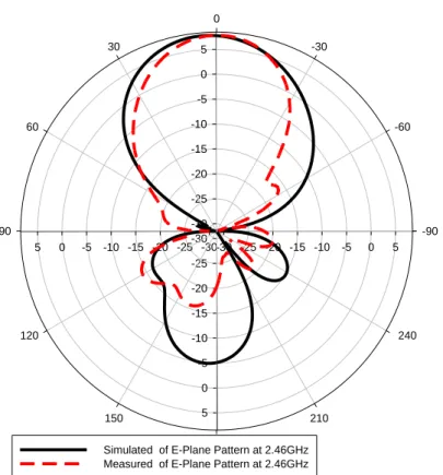
The fabricated of the sleeve dipole antenna array by print circuit board is shown in Fig 4.12. The substrate is FR4 with thickness 0.08 cm, The size is 16 cm in length and 2.1 cm in width. The height of the sleeve dipole antenna array to the reflector is about 2 cm. The simulation and measurement result of the reflection coefficient are shown in Fig. 4.14, whole bandwidth covers the operating frequency. The simulation and measurement results of efficiency are shown in Fig. 4.15. The measurement result of efficiency is about 60%. The simulation and measurement results of peak gain are shown in Fig. 4.16, the measurement result of peak gain is about 8.5 dBi. The simulation and measurement results of E-plane radiation pattern at 2.41 GHz are shown in Fig. 4.17. The simulation and measurement results of H-plane radiation pattern at 2.41 GHz are shown in Fig. 4.18.The simulation and measurement results of E-plane radiation pattern at 2.44 GHz are shown in Fig. 4.19. The simulation and measurement results of H-plane radiation pattern at 2.44 GHz are shown in Fig. 4.20. The simulation and measurement results of E-plane radiation pattern at 2.46 GHz are shown in Fig. 4.21. The simulation and measurement results of H-plane radiation pattern at 2.46 GHz are shown in Fig. 4.22. From E-plane, the simulation and measurement results are almost the same.
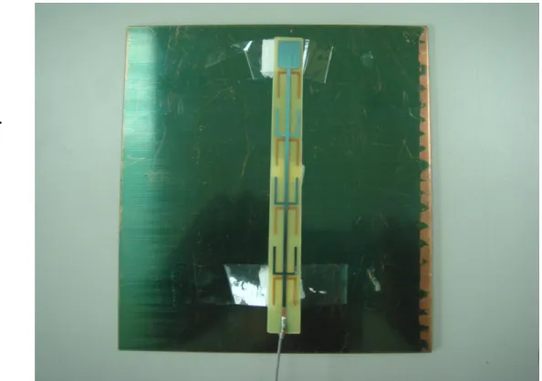
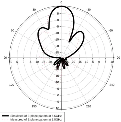
The fabricated of the sleeve dipole antenna array by print circuit board is shown in Fig. 4.23. The substrate is FR4 with thickness 0.08 cm, The size is 12.5 cm in length and 0.8 cm in width. The height of the sleeve dipole antenna array to the reflector is about 1 cm. The measurement environment is shown in Fig. 4.24. The simulation and measurement results of the reflection coefficient are shown in Fig. 4.25, whole bandwidth covers the operating frequency, the operate frequency of the fabricated of the sleeve dipole antenna array is shifting to high band. The simulation and measurement results of efficiency are shown in Fig. 4.26. The measurement result of efficiency is about 60%. The simulation and measurement results of peak gain are shown in Fig. 4.27, the measurement results of peak gain is about 10.2 dBi. The simulation and measurement results of E-plane radiation pattern at 5.2 GHz are shown in Fig. 4.28. The simulation and measurement results of H-plane radiation pattern at 5.2 GHz are shown in Fig. 4.29. The simulation and measurement results of E-plane radiation pattern at 5.5 GHz are shown in Fig. 4.30. The simulation and measurement results of H-plane radiation pattern at 5.5 GHz are shown in Fig. 4.31. The simulation and measurement results of E-plane radiation pattern at 5.8 GHz are shown in Fig. 4.32. The simulation and measurement results of H-plane radiation pattern at 5.8 GHz are shown in Fig. 4.33. From E-plane, the simulation and measurement results are different, the cause is the fabricated of the sleeve dipole antenna array is shifting to high band, so scan angle is different. H-plane has the same problem, too.
Design of the sleeve dipole antenna array by print circuit board for IEEE 802.11b/g, operate frequency is from 2.41 to 2.46 GHz. The height of the sleeve dipole antenna array to the reflector is about 2 cm. The gain of the sleeve dipole antenna array by print circuit board is about 8.5 dBi, and the efficiency is about 60%.
Design of the sleeve dipole antenna array by print circuit board for IEEE 802.11a, operate frequency is from 5.2 GHz to 5.8 GHz. The height of the sleeve dipole antenna array to the reflector is about 1 cm. The gain of the sleeve dipole antenna array by print circuit board is about 10.2 dBi, the efficiency of the sleeve dipole antenna array is about 60%. After optimization of antenna admittance, the peak gain has been increased 0.5dBi, the directivity has been increased 0.5dBi, and the efficiency also increased.
Fig. 4.1 WiFi apply in town
Top view
Bottom view
Fig. 4.2 Simulation model of sleeve dipole antenna array for IEEE 802.11b/g
Basic Station Client Client Client Client Client Client X X X X Y
a1, a2,..are insertion loss for individual dipole
Top view
Bottom view
Fig. 4.3 Simulation model of sleeve dipole antenna array for IEEE 802.11a
Fig. 4.4 Equivalent circuit of the sleeve dipole antenna array by print circuit board
X
Y X X X
Wavekength 0.01 0.02 0.03 0.04 Admit teranc e 0 5 10 15 20 25 30 35 40 Admittance Thickness: 0.4 mm
Fig. 4.5 Simulation result of admittance with thickness 0.08 cm
Fig. 4.6 Simulation result of admittance with thickness 0.04 cm D wavelength 0.01 0.02 0.03 0.04 Admit tance 0 2 4 6 8 10 Admittance Thickness: 0.8 mm D
Frequency (GHz) 5.0 5.2 5.4 5.6 5.8 6.0 |S 11| (d B) -25 -20 -15 -10 -5 0 Reference CASE 1 CASE 2 Reference CASE 1 CASE 2
Fig. 4.7 Simulation models of sleeve dipole antenna array by print circuit board
Frequency (GHz) 5.0 5.2 5.4 5.6 5.8 6.0 Ef fi cie nc y (Linear ) 0.0 0.2 0.4 0.6 0.8 1.0 Reference CASE 1 CASE 2 Frequency (GHz) 5.0 5.2 5.4 5.6 5.8 6.0 Directivity (d Bi) 5.5 6.0 6.5 7.0 7.5 8.0 8.5 Reference CASE 1 CASE 2
Fig. 4.9 Simulation results of efficiency
Frequency (GHz) 5.0 5.2 5.4 5.6 5.8 6.0 Peak Gain ( dBi) 3.0 3.5 4.0 4.5 5.0 5.5 6.0 Reference CASE 1 CASE 2
Fig. 4.11 Simulation results of the peak gain
Fig. 4.13 The measurement environment
Fig. 4.14 Simulation and measurement result of the reflection coefficient
Frequency(GHz) 2.0 2.2 2.4 2.6 2.8 3.0 |S 11|(dB) -30 -25 -20 -15 -10 -5 0 Simulated Measured
Frequency(GHz) 2.2 2.3 2.4 2.5 2.6 2.7 2.8 Ef fi cien cy (L inear ) 0.0 0.2 0.4 0.6 0.8 1.0 Simulated Measured Frequency(GHz) 2.2 2.3 2.4 2.5 2.6 2.7 2.8 Peak Gain( dBi) -10 -5 0 5 10 Simulated Measured
Fig. 4.15 Simulation and measurement result of efficiency
-30 -25 -20 -15 -10 -5 0 5 -30 -25 -20 -15 -10 -5 0 5 -30 -25 -20 -15 -10 -5 0 5 -30 -25 -20 -15 -10 -5 0 5 -90 -60 -30 0 30 60 90 120 150 180 210 240
Simulated of E-Plane Pattern at 2.41GHz Measured of E-Plane Pattern at 2.41GHz
-30 -25 -20 -15 -10 -5 0 5 -30 -25 -20 -15 -10 -5 0 5 -30 -25 -20 -15 -10 -5 0 5 -30 -25 -20 -15 -10 -5 0 5 -90 -60 -30 0 30 60 90 120 150 180 210 240
Simulated of E-Plane Pattern at 2.41GHz Measured of E-Plane Pattern at 2.41GHz
Fig. 4.17 Simulation and measurement result of E-plane pattern at 2.41 GHz
-30 -25 -20 -15 -10 -5 0 5 -30 -25 -20 -15 -10 -5 0 5 -30 -25 -20 -15 -10 -5 0 5 -30 -25 -20 -15 -10 -5 0 5 -90 -60 -30 0 30 60 90 120 150 180 210 240
Simulated of E-Plane Pattern at 2.44GHz Measured of E-Plane Pattern at 2.44GHz
-30 -25 -20 -15 -10 -5 0 5 -30 -25 -20 -15 -10 -5 0 5 -30 -25 -20 -15 -10 -5 0 5 -30 -25 -20 -15 -10 -5 0 5 -90 -60 -30 0 30 60 90 120 150 180 210 240
Simulated of H-Plane Pattern at 2.44GHz Measured of H-Plane Pattern at 2.44GHz
Fig. 4.19 Simulation and measurement result of E-plane pattern at 2.44 GHz
-30 -25 -20 -15 -10 -5 0 5 -30 -25 -20 -15 -10 -5 0 5 -30 -25 -20 -15 -10 -5 0 5 -30 -25 -20 -15 -10 -5 0 5 -90 -60 -30 0 30 60 90 120 150 180 210 240
Simulated of E-Plane Pattern at 2.46GHz Measured of E-Plane Pattern at 2.46GHz
-30 -25 -20 -15 -10 -5 0 5 -30 -25 -20 -15 -10 -5 0 5 -30 -25 -20 -15 -10 -5 0 5 -30 -25 -20 -15 -10 -5 0 5 -90 -60 -30 0 30 60 90 120 150 180 210 240
Simulated of H-Plane Pattern at 2.46GHz Measured of H-Plane Pattern at 2.46GHz
Fig. 4.21 Simulation and measurement result of E-plane pattern at 2.46 GHz
.
Fig. 4.23 Fabricated sleeve dipole antenna array by print circuit board
Fig. 4.24 Measurement environment of sleeve dipole antenna array by print circuit board
Frequency(GHz) 5.0 5.2 5.4 5.6 5.8 6.0 |s11 |(dB) -40 -35 -30 -25 -20 -15 -10 -5 0
simulated of return loss mearsured of return loss
Frequency(GHz) 4.6 4.8 5.0 5.2 5.4 5.6 5.8 6.0 Ef fi c ienc y (Line ar ) 0.0 0.2 0.4 0.6 0.8 1.0 Simulated of efficiency Mearsured of efficiency
Fig. 4.25 Simulation and measurement result of the reflection coefficient
Frequency(GHz) 4.6 4.8 5.0 5.2 5.4 5.6 5.8 6.0 P eak gain (dB i) 0 2 4 6 8 10 12
Simulated of peak gain Measured of peak gain
-30 -25 -20 -15 -10 -5 0 5 10 -30 -25 -20 -15 -10 -5 0 5 10 -30 -25 -20 -15 -10 -5 0 5 10 -30 -25 -20 -15 -10 -5 0 5 10 -90 -60 -30 0 30 60 90 120 150 180 210 240
Simulated of E-plane pettern at 5.2GHz Measured of E-plane pattern at 5.2GHz
Fig. 4.27 Simulation and measurement result of peak gain
-30 -25 -20 -15 -10 -5 0 5 -30 -25 -20 -15 -10 -5 0 5 -30 -25 -20 -15 -10 -5 0 5 -30 -25 -20 -15 -10 -5 0 5 -90 -60 -30 0 30 60 90 120 150 180 210 240
Simulated of H-plane pattern at 5.2GHz Measured of H-plane pattern at 5.2GHz
-25 -20 -15 -10 -5 0 5 10 -25 -20 -15 -10 -5 0 5 10 -25 -20 -15 -10 -5 0 5 10 -25 -20 -15 -10 -5 0 5 10 -90 -60 -30 0 30 60 90 120 150 180 210 240
Simulated of E-plane pattern at 5.5GHz Measured of E-plane pattern at 5.5GHz
Fig. 4.29 Simulation and measurement result of H-plane pattern at 5.2 GHz
-25 -20 -15 -10 -5 0 5 10 -25 -20 -15 -10 -5 0 5 10 -25 -20 -15 -10 -5 0 5 10 -25 -20 -15 -10 -5 0 5 10 -90 -60 -30 0 30 60 90 120 150 180 210 240
Simulated of H-plane pattern at 5.5GHz Measured of H-plane pattern at 5.5GHz
-30 -25 -20 -15 -10 -5 0 5 10 -30 -25 -20 -15 -10 -5 0 5 10 -30 -25 -20 -15 -10 -5 0 5 10 -30 -25 -20 -15 -10 -5 0 5 10 -90 -60 -30 0 30 60 90 120 150 180 210 240
Simulated of E-plane pattern at 5.8GHz Measured of E-plane pattern at 5.8GHz
Fig. 4.31 Simulation and measurement result of H-plane pattern at 5.5 GHz
-30 -25 -20 -15 -10 -5 0 5 -30 -25 -20 -15 -10 -5 0 5 -30 -25 -20 -15 -10 -5 0 5 -30 -25 -20 -15 -10 -5 0 5 -90 -60 -30 0 30 60 90 120 150 180 210 240
Simulated of H-plane pattern at 5.8GHz Measured of H-plane pattern at 5.8GHz
Chapter 5
Design of Planar Inverted F Antenna for HSDPA
In this chapter, design of the Planar Inverted F Antenna to applied in HSDPA. The operate frequencies are 850MHz、1900 MHz and 2100 MHz, in communication system, the space is very important, a planar inverted-F antenna will design to achieve multi-band and small size requirements.
5.1 Introduction of HSDPA
High-Speed Downlink Packet Access (HSDPA) is an enhanced 3G (third generation) mobile telephony communications protocol in the High-Speed Packet Access (HSPA) family, also called 3.5 G, which allows networks based on Universal Mobile Telecommunications System (UMTS) to have higher data transfer speeds and capacity. Current HSDPA deployments support down-link speeds of 1.8, 3.6, 7.2 and 14.0 Megabit/s. Further speed increases is available with HSPA, which provides speeds of up to 42 Mbit/s downlink and 84 Mbit/s with release 9 of the 3GPP standards.
The first phase of HSDPA has been specified in the 3rd Generation Partnership Project (3GPP) release 5. Phase one introduces new basic functions and is aimed to achieve peak data rates of 14.0 Mbit/s (see above). Newly introduced are the High Speed Downlink Shared Channels
(HS-DSCH), the adaptive modulation QPSK and 16QAM and the High Speed Medium Access protocol (MAC-hs) in base station.
The second phase of HSDPA is specified in the 3GPP release 7 and has been named HSPA Evolved. It can achieve data rates of up to 42 Mbit/s. It introduces antenna array technologies such as beam forming and Multiple-input multiple-output communications (MIMO). Beam forming focuses the transmitted power of an antenna in a beam towards the user’s direction. MIMO uses multiple antennas at the sending and receiving side. Deployments are scheduled to begin in the second half of 2008.
Further releases of the standard have introduced dual carrier operation, i.e. the simultaneous use of two 5 MHz carrier. By combining this with MIMO transmission, peak data rates of 84 Mbit/s can be reached under ideal signal conditions.
After HSPA Evolved, the roadmap leads to E-UTRA (Previously "HSOPA"), the technology specified in 3GPP Release 8. This project is called the Long Term Evolution initiative. The first release of LTE offers data rates of over 320 Mbit/s for downlink and over 170 Mbit/s for uplink using OFDMA modulation.
The planar inverted F antenna is changed from the inverted L antenna, which is introduction from the inverted L antenna. The structure of the monopole antenna and the inverted L antenna are shown in Fig 5.1, which can know the inverted L antenna is to combine the short monopole antenna with a ground. Generally, the length of the monopole antenna is H. The parameter H is about quarter-wavelength. The length of the inverted L antenna is L+A. The parameter L+A is about quarter-wavelength.
The advantages of the inverted L antenna are: (1)Small size
(2)Easy to produce
(3)The inverted L antenna and the monopole antenna are radiation pattern the same
Unfortunately, the disadvantage of the inverted L antenna is not easy to impedance match.
The structure of planar inverted F antenna is shown in Fig 5.2. The planar inverted F antenna is upgrade of the inverted L antenna, which has a transmission line connect to ground, so planar inverted F antenna can easy to impedance match.
In recent years, the planar inverted F antenna is widely applied in communication system. Because the advantages of the planar inverted F antenna are:
(1)Small size (2)Easy to produce
(3)The planar inverted F antenna and the monopole antenna are radiation pattern the same
(4) Easy to impedance match
5.3 Simulation of Planar Inverted F Antenna
This chapter design two type the planar inverted F antenna, the planar inverted F antenna A and the planar inverted F antenna B. The simulated model of the planar inverted F antenna A is shown in Fig 5.3. The substrate is FR4 with thickness 0.08 cm, the size is 4cm in length and 6cm in width. The transmission line A is resonance for 850 MHz, the transmission line B is resonance for 1900 MHz and 2100 MHz. The planar inverted F antenna is apply in communication system, the measurement environment has an iron pole, which the operate frequency will shifting to low band. So next is design the planar inverted F antenna B, the simulated model of the planar inverted F antenna B is shown in Fig 5.4. The simulation results of the reflection coefficient are shown in Fig 5.5. The planar inverted F antenna B has transmission line C, the transmission line C is resonance for 2100 MHz, the
5.4 Simulation and Measurement Results of Planar Inverted F
Antenna
The fabricated of the planar inverted F antenna B is shown in Fig 5.6. The substrate is FR4 with thickness 0.08 cm, The size is 4 cm in length and 6 cm in width. The measurement environment is shown in Fig 5.7. The simulation and measurement result of the reflection coefficient are shown in Fig 5.8, whole bandwidth covers the operating frequency. The simulation and measurement result of efficiency at low band are shown in Fig 5.9. The simulation and measurement result of efficiency at high band are shown in Fig 5.10. The measurement result of efficiency is about 40% at 850 MHz, and efficiency is about 60% at 1900 MHz and 2100 MHz. The simulation and measurement results of peak gain at low band are shown in Fig 5.11. The simulation and measurement results of peak gain at high band are shown in Fig 5.12. The measurement result of peak gain is about 1.5 dBi at 850 MHz, the measurement result of peak gain is about 2 dBi at 1900MHz and 2100MHz. The simulation and measurement result of 2D pattern in phi 0 deg at 850 MHz are shown in Fig 5.13. The simulation and measurement result of 2D pattern in phi 90 deg at 850 MHz are shown in Fig 5.14. The simulation and measurement result of 2D pattern in theta 90 deg at 850 MHz are shown in Fig. 5.15. The simulation and measurement result of 2D pattern in phi 0 deg at 1900 MHz are shown in Fig 5.16. The simulation and measurement result of 2D pattern in phi 90 deg at 1900 MHz are shown in Fig 5.17. The simulation and measurement result of 2D pattern in theta 90 deg at 1900 MHz
are shown in Fig 5.18. The simulation and measurement result of 2D pattern in phi 0 deg at 2100 MHz are shown in Fig 5.19. The simulation and measurement result of 2D pattern in phi 90 deg at 2100 MHz are shown in Fig 5.20. The simulation and measurement result of 2D pattern in theta 90 deg at 2100 MHz are shown in Fig 5.21.
5.5 Summary
This chapter design of planar inverted F antenna for HSDPA. The operate frequency are 850 MHz、1900 MHz and 2100 MHz. The antenna size is 4 cm in length and 6 cm in width. The measurement result of efficiency is about 40% at 850 MHz, the measurement result of efficiency is about 60% at 1900 MHz and 2100 MHz.
Fig. 5.1 Structure of the monopole antenna and the inverted L antenna
Fig. 5.2 Structure of planar inverted F antenna H A L Ground Ground L1 L2 H D
Fig. 5.3 Simulated model of the planar inverted F antenna A
圖 6.4 倒 F 型天線 B 之模擬結構圖
Fig. 5.4 Simulated model of the planar inverted F antenna B A
B
A
B C
Frequency(GHz) 0.8 1.0 1.2 1.4 1.6 1.8 2.0 2.2 |S 11|(dB) -40 -30 -20 -10 0 Antenna A Antenna B
Fig. 5.5 Simulation results of the reflection coefficient
Frequency(GHz) 0.8 1.0 1.2 1.4 1.6 1.8 2.0 2.2 |S 11|(dB) -40 -30 -20 -10 0 Simulated of S11 Measured of S11
Fig. 5.7 Measurement environment
Frequency(GHz) 0.80 0.85 0.90 0.95 1.00 Ef fi cie nc y (Linear ) 0.0 0.2 0.4 0.6 0.8 1.0 Simulated of Efficiency Measured of Efficiency Frequency(GHz) 1.9 2.0 2.1 2.2 Ef fi cie nc y (Linear ) 0.0 0.2 0.4 0.6 0.8 1.0 Simulated of Efficiency Measured of Efficiency
Fig. 5.9 Simulation and measurement result of efficiency at low band
Frequency(GHz) 0.80 0.85 0.90 0.95 1.00 Peak Gain( dBi) -20 -15 -10 -5 0 5
Simulated of Peak Gain Measured of Peak Gain
Frequency(GHz) 1.9 2.0 2.1 2.2 Peak Gain( dBi) -20 -15 -10 -5 0 5
Simulated of Peak Gain Measured of Peak Gain
Fig. 5.11 Simulation and measurement result of peak gain at low band
-40 -35 -30 -25 -20 -15 -10 -5 -40 -35 -30 -25 -20 -15 -10 -5 -40 -35 -30 -25 -20 -15 -10 -5 -40 -35 -30 -25 -20 -15 -10 -5 -90 -60 -30 0 30 60 90 120 150 180 210 240
Simulated of 2D pattern in phi0 at 850MHz Measured of 2D pattern in phi0 at 850MHz
-40 -35 -30 -25 -20 -15 -10 -5 -40 -35 -30 -25 -20 -15 -10 -5 -40 -35 -30 -25 -20 -15 -10 -5 -40 -35 -30 -25 -20 -15 -10 -5 -90 -60 -30 0 30 60 90 120 150 180 210 240
Simulated of 2D pattern in phi90 at 850MHz Measured of 2D pattern in phi90 at 850MHz
Fig. 5.13 Simulation and measurement result of 2D pattern in phi 0 deg at 850MHz
Fig. 5.14 Simulation and measurement result of 2D pattern in phi 90 deg at 850MHz
-40 -35 -30 -25 -20 -15 -10 -5 -40 -35 -30 -25 -20 -15 -10 -5 -40 -35 -30 -25 -20 -15 -10 -5 -40 -35 -30 -25 -20 -15 -10 -5 -90 -60 -30 0 30 60 90 120 150 180 210 240
Simulated of 2D pattern in theta 90 at 850MHz Measured of 2D pattern in theta 90 at 850MHz
-35 -30 -25 -20 -15 -10 -5 0 -35 -30 -25 -20 -15 -10 -5 0 -35 -30 -25 -20 -15 -10 -5 0 -35 -30 -25 -20 -15 -10 -5 0 -90 -60 -30 0 30 60 90 120 150 180 210 240
Simulated of 2d pattern in phi 0 at 1900MHz Measured of 2d pattern in phi 0 at 1900MHz
Fig. 5.15 Simulation and measurement result of 2D pattern in theta 90 deg at 850MHz
Fig. 5.16 Simulation and measurement result of 2D pattern in phi 0 deg at 1900MHz
-35 -30 -25 -20 -15 -10 -5 0 -35 -30 -25 -20 -15 -10 -5 0 -35 -30 -25 -20 -15 -10 -5 0 -35 -30 -25 -20 -15 -10 -5 0 -90 -60 -30 0 30 60 90 120 150 180 210 240
Simulated of 2D pattern in phi 90 at 1900MHz Measured of 2D pattern in phi 90 at 1900MHz
-40 -35 -30 -25 -20 -15 -10 -5 -40 -35 -30 -25 -20 -15 -10 -5 -40 -35 -30 -25 -20 -15 -10 -5 -40 -35 -30 -25 -20 -15 -10 -5 0 30 60 90 120 150 180 210 240 270 300 330
Simulated of 2D pattern in theta 90 at 1900MHz Measured of 2D pattern in theta 90 at 1900MHz
Fig. 5.17 Simulation and measurement result of 2D pattern in phi 90 deg at 1900MHz
Fig 5.18 The simulation and measurement result of 2D pattern in theta 90 deg at 1900MHz
-35 -30 -25 -20 -15 -10 -5 0 -35 -30 -25 -20 -15 -10 -5 0 -35 -30 -25 -20 -15 -10 -5 0 -35 -30 -25 -20 -15 -10 -5 0 -90 -60 -30 0 30 60 90 120 150 180 210 240
Simulated of 2D pattern in phi 0 at 2100MHz Measured of 2D pattern in phi 0 at 2100MHz
-35 -30 -25 -20 -15 -10 -5 0 -35 -30 -25 -20 -15 -10 -5 0 -35 -30 -25 -20 -15 -10 -5 0 -35 -30 -25 -20 -15 -10 -5 0 -90 -60 -30 0 30 60 90 120 150 180 210 240
Simulated of 2D pattern in phi 90 at 2100MHz Measured of 2D pattern in phi 90 at 2100MHz
Fig. 5.19 Simulation and measurement result of 2D pattern in phi 0 deg at 2100MHz
Fig. 5.20 Simulation and measurement result of 2D pattern in phi 90 deg at 2100MHz
-40 -35 -30 -25 -20 -15 -10 -5 -40 -35 -30 -25 -20 -15 -10 -5 -40 -35 -30 -25 -20 -15 -10 -5 -40 -35 -30 -25 -20 -15 -10 -5 -90 -60 -30 0 30 60 90 120 150 180 210 240
Simulated of 2D pattern in theta 90 at 2100MHz Measured of 2D pattern in theta 90 at 2100MHz
Fig. 5.21 Simulation and measurement result of 2D pattern in theta 90 deg at 2100MHz
Chapter 6
Conclusion
6.1 Summary
This thesis design the sleeve dipole antenna array, the print sleeve dipole antenna array, and the print sleeve dipole antenna array can combine reflector to increase directivity for IEEE 802.11 a/b/g.
First is design of the coaxial sleeve dipole antenna for IEEE 802.11 b/g. The peak gain of sleeve dipole antenna is about 1.9 dBi, the antenna efficiency is about 85%. The H-plane pattern is almost omni-direction. For long distance WiFi communication, the antenna gain is very important, the sleeve dipole antenna array is designed to enhance antenna gain. The peak gain of the coaxial sleeve dipole antenna array is about 4.2 dBi and the efficiency is about 90%, the H-plane pattern at is also omni-direction.
Second is design the sleeve dipole antenna by print circuit board for IEEE 802.11 a/b/g, the operate frequency is from 2.41GHz to 2.46 GHz. The height of the sleeve dipole antenna array by print circuit board to the reflector is about 2 cm. The gain of the sleeve dipole antenna array by print circuit board is about 8.5 dBi and the antenna efficiency of is about 60%.
For IEEE 802.11a, operate frequency is from 5.2 GHz to 5.8 GHz. The height of the sleeve dipole antenna array to the reflector is about 1 cm. The gain of the sleeve dipole antenna array by print circuit board is about 10.2 dBi and the antenna efficiency is about 60%. After optimization of antenna admittance, the peak gain has been increased 0.5 dBi, the directivity has been increased 0.5 dBi, and the antenna efficiency also increased.
Finally, design of the Planar Inverted F Antenna to apply to HSDPA. The operate frequencies are 850MHz、1900MHz and 2100MHz. The antenna size is 4 cm in length and 6 cm in width. The measured antenna efficiency is about 40% at 850 MHz, and 60% at 1900 MHz and 2100 MHz.
References
[1] GEMS, 3-D High Performance parallel EM simulation Software, www.2comu.com.
[2] R.S.Elliott “On the Design of Traveling-Wave-Fed Longitudinal Shunt
Slot Arrays “, IEEE TRANSACTIONS ON ANTENNA AND
PROPAGATION, VOL. AP-27,NO.5, SEPTEMBER 1979
[3]Wen-Shi Lee, Yi-Shien Chen, “900/1800MHz dual-band ceramic chip
antenna bandwidth improvement and equivalent circuit simulation and analysis” National Cheng Kung University, 2005
[4]Wenhua Yu, Xiaoling Yang, Yongjun Liu, Zheng (Warren) Li, Raj Mittra, Li (Racky) Li, Neng-Tien Huang, Electromagnetic Simulation Engineering [5] Yi-Chia Lin , Ching-Wen Hsue , “Design of Dual-Band Baluns and Their
Applications to Antenna Measurement” Matter Thesis National Taiwan
University of Science and Technology, 2006.
[6]Jung-Change, Chung-Ping Liu, “A study of printed inverted-F antenna in
WLAN band” Matter Thesis Yuan Ze University,2005
[7]Ya-Chung Yu, Jenn-Hwan Tarng, “The Miniaturization of the Multi-Band
Planar Inverted-F Antenna” Matter Thesis National Chiao Tung
University,2008
[8]Yen-Yu Chen, Kin-Lu Wong, “Novel Antenna Designs For A Pcmcia
Card” Matter Thesis National Sun Yat-Sen University,2003
[9]Chia-Yu Lee, Shyh-Jong Chung, “Design of On-Package Planar
Inverted-F Antenna for RF System-on-Package Application” Matter Thesis
[10]Chun-Lin Liu, Ching-Wen Hsue, “Dual-band Antennas Design for
Wireless Communication Applications” Matter Thesis National Taiwan
University of Science and Technology, 2004
[11]Yi-Chia Lin, Ching-Wen Hsue, “Design of Dual-Band Baluns and Their
Applications to Antenna Measurement” Matter Thesis National Taiwan
University of Science and Technology, 2007
[12]John D. Kraus, Ronald J. Marhefka, Antenna for All Applications, 2002 [13]Robert S. Elliott, Robert B. Collin, Antenna Theory and Design Revised
Edition
[14]Richard H. Chen, “Miniaturized Design of Microstrip-Fed Slot Antennas
for MIMO System Applications” Matter Thesis National Taiwan University,
附錄 已發表之研討會論文
[1] 張道治、陳俊傑、顏紹翔、陳晟瑋, “與背包或衣服相結合之DVB-T 天線設計”, 2009全國電信研討會, 2009
[2]Dau-Chyrh Chang, Chun-Chieh Chen, “The Performance Comparison of
the Sleeve Antenna and the Array Sleeve Antenna” AEM2C2010, 2010
[3] Dau-Chyrh Chang, Chun-Chieh Chen, “Optimization of Directivity for