行政院國家科學委員會專題研究計畫 成果報告
白光平面場放射光源之發光強度與發光均勻性改善
研究成果報告(精簡版)
計 畫 類 別 : 個別型 計 畫 編 號 : NSC 98-2221-E-151-005- 執 行 期 間 : 98 年 08 月 01 日至 99 年 07 月 31 日 執 行 單 位 : 國立高雄應用科技大學電子工程系 計 畫 主 持 人 : 楊素華 計畫參與人員: 碩士班研究生-兼任助理人員:黃思齊 碩士班研究生-兼任助理人員:杜其峰 碩士班研究生-兼任助理人員:徐家慧 碩士班研究生-兼任助理人員:蔡政勳 碩士班研究生-兼任助理人員:陳家興 報 告 附 件 : 出席國際會議研究心得報告及發表論文 處 理 方 式 : 本計畫涉及專利或其他智慧財產權,2 年後可公開查詢中 華 民 國 99 年 11 月 03 日
行政院國家科學委員會補助專題研究計畫
成 果 報 告
□期中進度報告
白光平面場放射光源之發光強度與發光均勻性改善
計畫類別:
個別型計畫
□整合型計畫
計畫編號:NSC 98-2221-E-151-005-
執行期間: 98 年 08 月 01 日至 99 年 07 月 31 日
執行機構及系所:國立高雄應用科技大學 電子系
計畫主持人: 楊素華
共同主持人:
計畫參與人員:黃思齊,杜其峰,徐家慧,蔡政勳,陳家興,李碩勛,吳婉伶
成果報告類型(依經費核定清單規定繳交):
精簡報告
□完整報告
本計畫除繳交成果報告外,另須繳交以下出國心得報告:
□赴國外出差或研習心得報告
□赴大陸地區出差或研習心得報告
出席國際學術會議心得報告
□國際合作研究計畫國外研究報告
處理方式:除列管計畫及下列情形者外,得立即公開查詢
涉及專利或其他智慧財產權,□一年
二年後可公開查詢
中
華
民
國
99
年
10
月
16 日
白光平面場放射光源之發光強度與發光均勻性改善
楊素華,黃思齊,杜其峰,徐家慧,蔡政勳,陳家興,李碩勛,吳婉伶 國立高雄應用科技大學 高雄市 807 建工路 415 號 Tel: +886-7-3814526-5631 Fax: +886-7-3811182 中文摘要 本實驗探討平面場放射光源之發光強度及發射電子均勻性的改善;同時,為製作白光場放射光源, 白光螢光粉利用了固態反應法合成。實驗中發現,Zn/ZnOx之蒸氣濃度、奈米結構之主要成長面、以及 掺質之化學活性對 ZnO 奈米結構之表面型態及電子放射能力均影響甚大。當石墨原料的溫度增加時, ZnO 奈米線的直徑增加且針狀的型態也轉為葉片狀的奈米結構。於 N2/O2流量比 7:4 及溫度 900°C 下成 長 10 分鐘,則所成長的 ZnO 奈米結構均勻分佈,此時可獲得最佳場放射特性,其臨界電場為 0.34 V/μm;於電場 7.59 V/μm時,其電流密度約為 0.24 mA/cm2;元件的 CIE 彩色坐標位於(0.35, 0.37),為 近白光。對平面場放射光源之發光強度,色純度,及發射電子之均勻性,我們將持續加以研究,若有 新的研究成果亦會加以發表及分享。 ABSTRACTIn this proposal, the improvements on the luminance intensity and the electron emission uniformity of the field-emission lighting were investigated; in the meantime, the white-light phosphor was synthesized by solid-state reaction for the preparation of white-light flat-panel field-emission lighting. It was found that the Zn/ZnOxvapor concentration, the dominant growth plane of the nanostructure, and the chemically activity of
dopants had strong effects on the morphology and emission ability of ZnO nanostructures. The diameters of the ZnO nanostructures were increased and the morphologies of nanoneedles were transformed into leaves-like nanostructure when the graphite temperature was increased. The optimal field emission property of the ZnO nanostructure was achieved when they were grown at 900°C for 10 min under N2/O2flow ratio of 7:4.
The turn-on field for field emission was 0.34 V/μm,thecurrentdensity atan electricfield of7.59 V/μm was 0.24 mA/cm2, and the CIE coordinates were x = 0.35, y = 0.37, it was a near white light. The improvements on the luminance intensity, color purity, and emission uniformity of electrons of the field-emission lighting will be keeping studied after this proposal.
INTRODUCTION
Flat-panel field emission lighting makes use of cold-cathode emission, and presents many advantages, such as lighter weight, wider viewing angle and better image quality [1]. The structure of FED contains field emission tips and phosphor screen. Field emission phenomenon first received attention in 1961 when Shoulder proposed the first vacuum microelectronics device which was subsequently developed by Spindt and co-workers [2-4]. Many different shapes of emission tips have been investigated in terms of the feasibility of reducing the operating voltage and fulfilling the requirements of a flat-panel display. All tip shapes have their own characteristics and unexpected performances. Nowadays, the tips with nanostructures have been attracted much attention.
For nanostructured tips, the unique and fascinating properties of ZnO nanostructures, particularly their electronic and optical properties, have recently gained prominence because of their potential applications in transparent electronic devices [5], flat-panel displays [6], and electrochemical and toxic-gas sensors [7-9]. ZnO nanostructures can be synthesized by various methods, such as pulsed laser deposition [10], metalorganic chemical vapor deposition [11], sputtering [12], and oxidation [13]. Among these growth techniques, the
oxidation technique is the most commonly used for the preparation of ZnO nanostructures. In this simple and low-cost synthesis process, the properties of ZnO nanostructures are significantly affected by the growth temperature, growth time, and the composition of the vapor phase.
Typically, undoped ZnO nanostructures are n-type, which is attributed to excess electrons introduced by the presence of oxygen vacancies and Zn interstitials in the crystal. The characteristics of ZnO nanostructures can be modified by thermal treatment or by the appropriate doping of cationic substituents. Doping with trivalent In, Ga, and Al atoms or monovalent Li atoms is commonly considered to be the most effective method of modifying the optical and electrical properties of ZnO nanostructures. These methods can cause considerable changes to the crystallization, morphology, and growth mechanism of ZnO nanostructures [14-19].
To date, white-light phosphors have attracted significant attention due to their applications as backlights and light sources. To prepare stable white-light phosphors exhibiting high luminance, oxide-based materials are preferred [21-23] because they have unique physical and chemical properties, high stability, and satisfactory broadband emission in the visible light region. To increase the luminescence efficiency of phosphor, researchers have tried various approaches. These include using different synthesis methods to modify phosphor particle size and surface morphology; adding conductive materials to increase the conductivity [24, 25]; mixing flux materials to increase the extent of crystallization [26]; and doping a sensitizer to enhance excitation energy absorption and energy transfer to the activator [27]. By choosing a suitable synthesis method, we can achieve high efficiency along with the desired emission color of the phosphor.
In this study, ZnO nanostructures were synthesized by the vapor-phase growth mechanism. The mixing ratio of zinc oxide to graphite was varied in order to determine the optimal composition of the source material for obtaining ZnO tips with optimal properties. Meanwhile, the solid-state sintering method was used to synthesize the phosphors. The electron emission uniformity and the luminescence intensity of the white-light FED were investigated.
EXPERIMENTS
The ZnO nanostructures were fabricated via a simple vapor-phase transport process in a conventional furnace, with a horizontal quartz tube of 4 cm inner diameter. A mixture of commercially available ZnO (99.995%) and graphite (99.999%) powders was used as the source material and was placed in an alumina boat. A p-type (100) Si wafer with a resistivity of 10 Ω·cmwas used as the substrate. A 7-nm-thick Ag film, composed of nanosized islands, was deposited on Si by thermal evaporation, which served as the catalyst. The substrate was placed directly above the source powder but separated by approximately 0.5 cm. Synthesis was carried out at a temperature of 1000oC for 1 h in a N2/O2 atmosphere. The supply of O2 gas was turned on
when the substrate temperature reached 950oC and was turned off when the substrate temperature cooled to 950oC. After the growth, a light gray layer was found on the surface of the substrate. Furthermore, the effect of doping cationic substituents on the properties of nanostructures was studied. The morphological and crystalline properties of the nanostructures were characterized by X-ray diffraction [XRD; SIEMENS D5000, with Cu Kα radiation (λ = 0.1541 nm)], field-emission scanning electron microscopy (FE-SEM; Philips XL40), energy-dispersive X-ray analysis (EDX), transmission electron microscopy (TEM; FEI Tecnai F20 G2 MAT S-TWIN), and selected-area electron diffraction (SAED). Photoluminescence (PL) (Hitachi F-7000) was used to measure the optical properties of the nanostructures, and a high-vacuum system (10-5 Torr) was used to measure the FE property.
In addition, For the preparation of white-light phosphor, oxide and sulfide powers were used as the source materials, which were doped with different activator at different concentrations. The mixed powders were blended with deionized water then milled for 24 h. Subsequently, the solution was dried in an oven and sintered at 700−1200°C for 1−8 h. Finally, the synthesized powders were ground, and the white-light phosphor was prepared. The surface morphology of the phosphor was visualized by SEM. The luminescence characteristics of phosphors were evaluated with the PL and PL excitation (PLE)measurements. The luminanceand Commission Internationaledel’Eclairage(CIE)coordinatesof the phosphor were measured using a Minolta Chroma Meter model CS-100A. A 6-W UV lamp (1200 μW/cm2, wavelength of 254 nm) was used as the excitation source for luminance measurements.
Results and Discussion
During the synthesis, graphite reduced ZnO into Zn metal by the processes ZnO + C → Zn + CO, 2ZnO + C → 2Zn + CO2, and ZnO + CO → Zn + CO2. At the same time, the oxidation processes Zn + CO2→ ZnO
+ CO, Zn + 0.5xO2 → ZnOx, and 2C + 1.5O2 → CO + CO2 also occurred.17) At the growth temperature of
1000oC, Zn and Zn suboxides should be in their vapor phase.18,19) The Ag nanograins forming small solid islands on the Si surface obstructed the flow of Zn and ZnOx vapors. This promoted the absorption of
Zn/ZnOx on the surface of the Ag nanograins, the development of nucleation sizes, and self-catalyzation to
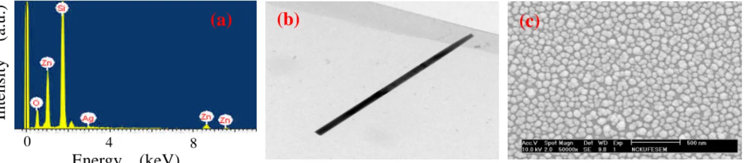
form ZnO nanoparticles. EDX analysis showed that the ZnO nanostructures consisted of only Zn and O [Fig. 1(a)]. The detected elements of Si and Ag were from the substrate and Ag film, respectively. No Ag nanoparticle at the tip of each nanorod was observed, as shown in the TEM image of Fig. 1(b). However, the deposition of Ag nanograins was crucial to the growth of ZnO nanostructures at the high temperature of 1000oC. This is because the Zn atoms, with a boiling point of 907oC,19)can remain on the substrate for only a very short time when there are no special nucleation sites on the substrate, that is, Zn atoms are reevaporated from the substrate without being oxidized, and nothing is grown on the bare Si substrate. Therefore, the deposited Ag film acted as a catalyst, which enhanced the growth of ZnO nanostructures. An SEM image of the as-deposited Ag film is shown in Fig. 1(c).
Figure 1. (a) EDX analysis and (b) TEM image of the ZnO nanorods. (c) SEM image of the as-deposited Ag film.
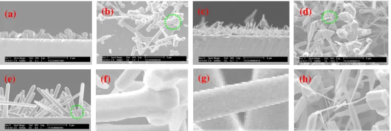
Since the concentration of Zn vapor has a strong effect on the morphology of ZnO nanostructures, the composition of the source powder is one of the key parameters in nanostructure growth. When the concentration of ZnO was lower than that of graphite, such as for a weight ratio of ZnO/C = 3/7, the growth of ZnO nanorods was slow, and the nanorods had a hexagonal nanobrick structure, as exhibited in Figs. 2(a) and 2(b). Figure 2(f) is an enlargement of the region of Fig. 2(b) in the green dotted circle. From Fig. 2(f), we can see that the nanorod grew from the base of a nanobrick, and that when the growth time was prolonged, the nanobrick became dispersed and a long nanorod was grown. The XRD pattern shows that the dominant growth plane of ZnO nanorods was the (002) plane; hence, most of the nanorods grew perpendicularly to the substrate. The growth rate of the ZnO nanorods increased when the weight ratio of ZnO/C was increased to 1, which was attributed to the increased Zn and ZnOxvapor concentrations.
We found that the nanorods had a tapered stem with a hexagonal cross section and that a long nanowire grew from the top of each nanorod [Figs. 2(c) and 2(d)). Fig. 2(g) is an enlargement of the region of Fig. 2(d) in the green dotted circle. It was also found that when a new nucleation site was formed on the nanorod, a hexagonal-faceted nanobrick developed, and consequently, a branched nanorod grew. In addition, when the supply of O2 gas was turned off after growth, the O2 that remained in the reactor chamber was gradually
exhausted and the vapor concentration decreased as time passed. In this situation, the local concentration of Zn on the growth front may have been very high, which led to rapid growth in the longitudinal direction and continued growth during the cooling period. This is why a thin and long nanowire grew from the top of each nanorod, as shown in Fig. 2(d).
Moreover, when the weight ratio of ZnO/C was increased to 7/3, the high ZnO vapor concentration enhanced the growth rate of the nanorods, and the branches disappeared. The hexagonal cross section of the tapered nanorods with a screw-dislocation morphology was clearly observed, as shown in Fig. 2(e). Figure 2(h) is an enlargement of the region of Fig. 2(e) in the green dotted circle, showing the screw-dislocation morphology of the nanorods. The nanorods were approximately 1 μm in diameterand 10.6 μmin length.
In te n si ty (a .u .) 0 4 8 (a) Energy (keV) (b) (c)
Figure 2. SEM images of the ZnO nanorods synthesized at various weight ratios of ZnO/C; (a) 3/7, (b) 1/1, and (c) 7/3. The high-magnification SEM images are inserted.
Figure 3(a) shows a TEM image of a ZnO nanorod with a tapered morphology. This image revealed that no droplet of Ag/Zn alloy was present on the nanotip. The high-resolution TEM (HRTEM) photograph of the nanorod displayed in Fig. 3(b) shows that it has a hexagonal wurtzite ZnO structure growing along the [002] direction with a lattice spacing of 0.25 nm. The SAED pattern shown in Fig. 3(c) was taken from the same area of the ZnO nanorod as that shown in the HRTEM image. The pattern was indexed on the basis of a hexagonal cell with lattice constants of a = b = 3.26 A。and c = 5.22 A。, consistent with the XRD result. This demonstrates that the nanorods were single-crystal wurtzite ZnO.
Figure 3. (a) TEM, (b) HRTEM, and (c) SAED images of the ZnO nanorod.
To investigate the effect of the In2O3doping concentration on the formation of ZnO nanostructures, the
weight ratio of ZnO/C was fixed at 7/3 while the concentration of In2O3 was varied from 0 to 9 wt%. It was
found that when the ZnO was doped with In2O3, the dominant growth plane of the nanostructures was altered
from (002) to (101). As a result, the growth of hexagonal ZnO nanobricks was slow, and the morphology of the nanostructures changed from a tapered nanorod at an In2O3 doping concentration of 0 wt% to a
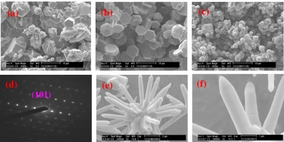
hexagonal-faceted prismatic nanobrick at 1 wt%, a hexagonal-faceted nanodisk at 5 wt%, and an aggregated nanoball at 9 wt% (Fig. 4). The thicknesses of the nanobricks and nanodisks were approximately 2.22 and 0.67 μm at In2O3concentrations of 1 and 5 wt%, respectively, as shown in Figs. 4(a) and 4(b). The nanodisks
were observed to aggregate into clusters to form nanoballs when a high In2O3 concentration of 9 wt% was
doped [Fig. 4(c)]; the grain size of the nanoballs was about2.24 μm.The full width at half maximum (FWHM) values of the XRD (101) main peak were 0.22, 0.24, and 0.25o for In2O3 concentrations of 1, 5, and 9 wt%,
respectively. The decay of crystallinity was induced when In ions substituted for Zn; an increased FWHM of the XRD (101) main peak was thus observed. However, the single-crystal ZnO:In nanoballs grew with a hexagonal wurtzite structure, as shown by the SAED image in Fig. 4(d).
Furthermore, the synthesized ZnO:Ga nanorods exhibited a hexagonal wurtzite structure with measured
(a) (b) (c) (d) [002] 2.5 A。 (001) (a) (b) (c) (e) (f) (g) (h)
lattice constants of a = b = 3.24 Å and c = 5.21 Å. The (002) plane was the main growth plane of the ZnO:Ga nanorods. No diffraction peaks corresponding to Ga-compound phases were observed.
In contrast to the ZnO and ZnO:In nanostructures, the ZnO:Ga nanostructures had a sea-urchin-like morphology. Straight ZnO:Ga nanorods with a sharp end grew radially from the same root. An SEM image of the ZnO:Ga nanorods is shown in Fig. 4(e). When the concentration of Ga2O3 was increased from 0.5 to 8
wt%, the diameter of the ZnO:Ga nanorods was decreased from 700 to 500 nm but their length was increased from 3 to 7 μm.
Additionally, in contrast with the hexagonal prism ZnO nanorods, the ZnO:Ga nanorods in the sea-urchin-like structure had a smooth hexagonal surface. The high-magnification SEM image shown in Fig. 4(f) indicated that the ZnO:Ga nanorods were grown with a screw-dislocation or stacked structure resulting from the stress induced by Ga doping. The Zn ions (RZn2 = 0.074 nm) in the ZnO lattice can be substituted by Ga ions (RGa3 = 0.062 nm), which induces structural stress as well as extra electrons in the crystal, thereby increasing the conductance of the nanorods; this is a desirable characteristic for nanorods used as field emitters.
Figure 4. SEM images of the ZnO:In nanostructure synthesized at various In2O3doping concentrations; (a) 1,
(b) 5, and (c) 9 wt%. (d) SAED image of the ZnO:In nanoball; (e) SEM and (f) high-magnification SEM images of the ZnO:Ga nanorods.
Figure 5. Schematic diagram of the growth mechanisms of the ZnO, ZnO:In, and ZnO:Ga nanostructures.
The growth mechanisms for the ZnO, ZnO:In, and ZnO:Ga nanostructures are schematically illustrated in Fig. 5. For the synthesis of ZnO nanostructures, ZnO powder was first heated and reacted with graphite to generate Zn vapor, which then reacted with oxygen to create ZnOx vapor. Zn and ZnOx adsorbed on the
surface of Ag grains and self-catalyzed to form ZnO nanoparticles. As the growth process proceeded, nanobricks with a hexagonal structure then developed. When the concentration of ZnO was increased, the Zn
(a) (b) (c) (d) (e) (f) (101) ZnO ZnO:In ZnO:Ga ZnO↑ ZnO↑ In2O3↑ time↑ nucleus
and ZnOx vapor concentrations were subsequently increased; this led to nanorod growth from the base of the
nanobrick, and at higher ZnO concentrations, the nanobricks became dispersed and long nanorods were grown. Furthermore, from the viewpoint of surface energy, the lowest-energy facets for ZnO are {0001}, followed by {1010} and {1011}. Thus, faceted, single-crystal ZnO hexagonal disks tended to form, enclosed by {0001} top and bottom surfaces and {1010} side surfaces. The Zn surface with the lowest-energy {0001} facets tended to be the most stable and were able resist oxidation, whereas the higher-energy {1010} surfaces were oxidized more rapidly. As a result, the side surfaces of the hexagonal nanodisks were oxidized first. Faster growth along the c axis direction led to the nanodisks growing into nanobricks and then into nanorods with increasing concentration of ZnO. In addition, the growth rate of the planes follows the sequence (0001) > (1010) > (1011); the faster a crystallographic face grows, the faster it disappears. Consequently, the prism nanorods had a tapered hexagonal end.
When ZnO was doped with In2O3, (101) was the dominant growth plane, and the growth along the c axis
was slow; therefore, the ZnO:In nanostructures had a nanodisk morphology at the beginning of growth. During the growth, Zn ions were substituted by In ions (RIn3 = 0.080 nm) owing to their similar ionic radius. The reactivity of an element generally decreases as the Pauling electronegativity of the atom increases. From this viewpoint, In is less chemically reactive than Zn because the Pauling electronegativities of In and Zn are 1.78 and 1.65, respectively. Consequently, the growth rate of the nanodisks was decreased and the morphology of the nanostructures was changed from hexagonal-faceted nanodisks to aggregated nanoballs when the In2O3doping concentration was increased.
On the other hand, for the growth of ZnO:Ga nanostructures, it is thought that microsized Zn droplets were formed on the Ag-deposited Si substrate. Then, oxygen reacted with Zn, resulting in the development of many ZnO nuclei on the droplet. Zn can be considered to be more chemically reactive than Ga because the Pauling electronegativity of Ga, 1.81, is higher than that of Zn. Therefore, Ga possessed a configuration-limiting ability, preventing Zn from three-dimensional nucleation. Consequently, the tiny Zn nuclei grew radially to form one-dimensional hexagonal nanorods. Furthermore, inasmuch as the Zn-terminated (0001) surface is more chemically reactive than the O-terminated (0001) surface, the enriched Zn atoms on the (0001) surface formed screw dislocations and led to the rapid growth of nanorods by a self-catalytic process.
The optical properties of the nanostructures are measured. It was found that at a high concentration of graphite, for example, a weight ratio of ZnO/C = 3/7, the graphite reacted with oxygen to form CO and CO2
gases, resulting in a higher concentration of oxygen vacancies and leading to high-intensity bluish-green emission. When the weight ratio of ZnO/C was increased to 7/3, the increased Zn and ZnOx vapor
concentrations improved the crystallinity of ZnO nanorods; hence, a significant decrease in the intensity of the bluish-green emission was observed. On the other hand, the emission originating from structural defects was enhanced for the ZnO:In nanoballs and ZnO:Ga nanorods; as a result, broad PL spectra were observed. The intensity of emission from the ZnO:In nanoballs was decreased when the doping concentration of In2O3was
increased, whereas it was enhanced when the doping concentration of Ga2O3was increased. In2O3 and Ga2O3
doping appeared to improve the PL intensity of the ZnO nanostructures, and the highest PL intensity was obtained from the ZnO:Ga nanorods.
0 2 4 6 8 0.0 0.2 0.4 0.6 C u rr en t D e n si ty (m A /c m 2 ) Electric Field (V/ m) ZnO tips ZnO:In tips ZnO:Ga tips
Figure 6. (a) Field emission characteristics of the ZnO, ZnO:In, and ZnO:Ga nanostructures. The performance image and the CIE coordinates of the white-light flat-panel field-emission lighting are shown in Figs. 6(b) and 6(c), respectively.
(a) (b)
Figure 6(a) shows the FE characteristics of the nanostructures. The FE characteristics of the ZnO nanorods, ZnO:In nanoballs, and ZnO:Ga nanorods satisfied the Fowler-Nordheim (FN) relationship, with field enhancement factors β of 1512, 1283, and 2379, respectively. The emission current density of the ZnO:Ga nanorods was higher than those of the ZnO nanorods and ZnO:In nanoballs. The formation of the nanoball structure does not appear to improve FE performance. The performance image and the CIE coordinates of the white-light flat-panel field-emission lighting are shown in Figs. 6(b) and 6(c), respectively; the CIE coordinates were x = 0.35, y = 0.37. The emission area of FED was 2×2 cm2.
In order to improve the luminescence intensity and emission uniformity of the white-light flat-panel field-emission lighting, the emission tips of ZnO nanostructures were grown using a three-zone horizontal furnace via vapor transport deposition process. After the deposition of Au-catalyst thin film, commercial Zn powder and graphite powder (weight ratio = 1:1) were loaded into two alumina boats. The Au-catalyst deposited substrate was placed just above the other alumina boat. Then, the powder sources and the substrate were put into different heating zones of the tube furnace. Additionally, the graphite powder was placed in the first zone, zinc powder was in the second heating zone, and the substrate was put into the third zone. The first zone was the upstream region near to the gas inlet and the third zone was the downstream region far from the gas inlet. In this experiment, nitrogen gas is used as the carrier gas and oxygen gas is the reactive gas. Meanwhile, a constant nitrogen gas was flowed in the tube furnace. When the reaction started, the oxygen gas was introduced into the furnace to react with zinc. The supply of oxygen gas was cut off after the reaction, and the furnace was cooled down to room temperature.
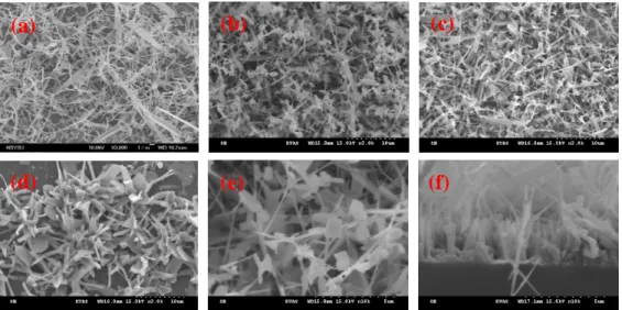
Figure 7. SEM photos of ZnO nanostructures with different graphite temperatures of 850–1000oC. Top views (3000 X) for (a) 850, (b) 900, (c) 950, and (d) 1000oC. The high resolution and cross sectional views (10000 X) of nanostructures were shown in (e) and (f) for graphite temperature of 900oC.
First, the weight ratio of ZnO and graphite powder was fixed at 0.5:0.5, and the flow rates of N2and O2
gases were set at 70 and 40 sccm, respectively. To study the effect of the temperature of graphite on the growth of ZnO nanostructures, the temperatures of graphite were varied at 850–1000°C to synthesize ZnO nanostructure on (100) Si substrate. The N2 gas and O2 gas were set at 70 and 30 sccm, respectively. The
temperature rising rate of the tube furnace was controlled at 40 °C/min and the growth time was 10 min. Figure 7 shows the SEM photos for nanostructures grown on Si substrate; top view 3000 X for (a) 850, (b) 900, (c) 950, and (d) 1000 °C. When the temperature was 850°C, the ZnO nanostructures with morphologies of narrow diameter and long length were observed because the ZnO nanostructures grown at relatively low temperature are too long to stand straightly. When the first zone temperature increased, the reaction was also increased and the ZnO nanostructures with wider diameter and shorter length were grown. Because of the high temperature, the length of ZnO nanostructures was broken and the thickness of ZnO layer was increased. However, the strongest reaction was occurred when the temperature of first zone was 1000°C, and the ZnO nanostructure with the widest diameter and shortest length were grown, as show in Fig. 7(d). The high resolution top view and cross sectional view 10000 X for 900°C are shown in Figs.7(e) and (f), respectively.
(a) (b) (c)
Figure 8 shows the SEM photographs for ZnO nanostructures grown on Si substrate with different weight ratios of Zn to graphite powders; top view 3000 X with (a) 1:1, (b) 7:5, and (c) 2:1 for three samples. The diameters of ZnO nanostructures shown in Figs. 8(a), (b), and (c) were 0.7, 1, and 1.3 μm, respectively. In addition, lengths of the nanostructures were 22, 9.2, and 4.4 μm for nanostructures grown at different weight ratios of 1:1, 7:5, 1:2, respectively. In Fig.8, it is found that a small amount of nanostructure was grown due to the deficiency of Zn powders. On the other hand, the quantity of the ZnO nanostructures was increased when the weight ratio of Zn powder was increased. The ZnO nanostructures had perfect length and diameter when the weight ratio of Zn to graphite powders was 1:1. Once an excess of Zn powder was used, the lengths of nanostructures were decreased and the diameters were increased.
Figure 8. SEM photographs for ZnO nanostructures grown on Si substrate with different weight ratios of Zn to graphite powders; top view 3000 X for (a) 1:1, (b) 7:5, and (c) 2:1.
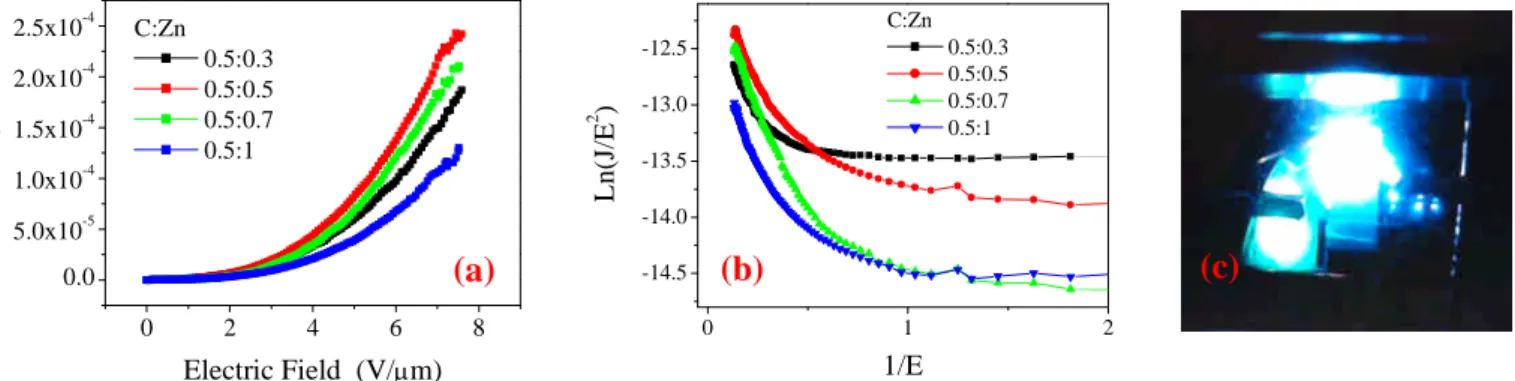
Figure 9(a) displays the field emission J-E plots of the nanostructures for the different weight ratios of Zn and graphite of 3:5, 1:1, 7:5, and 2:1. The J-E curves were measured with an ITO anode and the spacing between emitter to anode was 145 μm. The measurements were carried out at room temperature in 5×10⁻⁶Torr. The electron emission turn-on fields, defined as the emission current density reaching 0.1 μA/cm2, were about 0.27, 0.34, 0.48, and 0.47 V/μm for different Zn to graphite weight ratios of 3:5, 1:1, 7:5, and 2:1.
After the I-V properties were measured, the Fowler-Nordheim (F-N) relationship of ln(J/E2) is plotted as a function of (1/E) in order to realize the field emission properties of the nanostructures. The inset shown in Fig. 9(b) is the corresponding Fowler-Nordheim (F-N) plot. The values of field enhancement factor βwere about 1093, 1509, 1303, and 1051 for nanostructures grown for Zn to graphite weight ratios of 3:5, 1:1, 7:5, and 2:1, respectively. Obviously, as the Zn to graphite weight ratio was 1:1, the optimal ZnO nanostructure was obtained and a higher field enhancement factor βwas obtained. The performance image of the near white-light flat-panel field-emission lighting is shown in Fig. 9(c).
0 2 4 6 8 0.0 5.0x10⁻⁵ 1.0x10⁻⁴ 1.5x10⁻⁴ 2.0x10⁻⁴ 2.5x10⁻⁴ (a) C:Zn 0.5:0.3 0.5:0.5 0.5:0.7 0.5:1 C u rr en t D en si ty (A /c m 2 ) Electric Field (V/m) 0 1 2 -14.5 -14.0 -13.5 -13.0 -12.5 (b) C:Zn 0.5:0.3 0.5:0.5 0.5:0.7 0.5:1 L n (J /E 2 ) 1/E
Figure 9. (a) J-E plots and (b) F-N plots of the ZnO nanostructures for different C/Zn weight ratios; (c) the performance image of the near white-light flat-panel field-emission lighting.
CONCLUSIONS
In this study, we found that the Zn/ZnOx vapor concentration, the dominant growth plane of the
nanostructure, and the chemically activity of dopants had a strong effect on the morphology of ZnO nanostructures.When the nanostructures were grown with a three-zone furnace, it was found that when the graphite temperature was increased, the diameters of the ZnO nanostructures were increased and the
(a) (b) (c)
morphologies of nanoneedles were transformed into leaves-like nanostructure. The best emission property of the ZnO nanostructure was achieved when they were grown at 900°C. Additionally, the quantity of nanoneedles was increased when the oxygen flow ratio was increased, whereas the diameter of nanoneedles was decreased. Therefore, the field emission property of nanostructures was improved when they was grown with increased oxygen flow ratio because high density of emitters and uniform nanoneedle arrays were grown except that the oxygen flow ratio was 50 sccm. It is shown that when the needle-like nanostructures were grown at optimal conditions, the turn-on electricfield forfield emission was0.34 V/μm,thecurrentdensity at an electricfield of7.59 V/μm was0.24 mA/cm2
for ZnO nanostructures grown at 900°C for 10 minutes. In this study, the emission uniformity of electrons was successfully achieved with a three-zone furnace by varied the power source weight ratio, gas flow ratio, furnace heating rate, and synthesis temperature. A near white-light flat-panel field-emission lighting was obtained when the white phosphor was adopted. The improvements on the luminance intensity, color purity, and emission uniformity of electrons of the field-emission lighting will be keeping studied.
ACKNOWLEDGEMENTS
The authors thank the National Science Council of the Republic of China for financially supporting this work under contract No. NSC 98-2221-E-151-05.
JOURNAL PAPERS
1. Su-Hua Yang, Fu-Shou Tsai, Jia-Xing Chen, “Characterizations of white-light ZnWO4phosphor prepared
by blending complementary phosphor”, Journal of Solid State Electrochemistry,14, p.937-943 (2010). 2. Su-Hua Yang, Yu-Jiu Lial, Nai-Jen Cheng, Yin-Hsuan Ling, “Preparation and characteristics of yellow
ZnS:Mn,Ce phosphor”, Journal of Alloys and Compounds, 489, P. 689-693, 2010.
3. Su-Hua Yang, Sheng-Yu Hong, Cheng-Hsun Tsai, “Growth mechanisms and characteristics of ZnO nanostructures doped with In and Ga”, Japanese Journal of Applied Physics, 49(6), 06GJ06, 2010.
4. Su-Hua Yang, Chien-Hung Wang, Yin-Hsuan Ling, “Photoluminescence ofwhiteZnS-based phosphor with Pr and Mn activators prepared by complementary blending and codoping”, Solid State Sciences, Sep. 2010. (under revised)
CONFERENCE PAPERS
1. Su-Hua Yang, Sheng-Yu Hong, Cheng-Hsun Tsai, Shuo-Xun Li, “Growth mechanism and characteristics of ZnO nanostructures doped with In and Ga”, 2009 International Microprocesses and Nanotechnology Conference, Sapporo, Japan, November 16-19, 2009.
2. Cheng-Hsun Tsai, Shuo-Xun Li, Su-Hua Yang, “Crystalline and optical properties of ZnO:Ga nanostructures prepared with different temperature raising rates by vapor-phase transport”, 2009 MRS-T Annual Meeting, Hualien, Taiwan, Nov. 26-28, 2009.
3. Jia-Xing Chen, Su-Hua Yang, Woan-Ling Wu, “Preparation and improvement in luminescence property of K+-doping on the properties of ZnWO4 phosphor”, 2009 MRS-T Annual Meeting, Hualien, Taiwan,
Nov. 26-28, 2009.
4. Chian-Hung Wang, Yin-Hsuan Ling, Su-Hua Yang, “Photoluminescence properties of white-light ZnS phosphors doped with different dopants”, 2009 MRS-T Annual Meeting, Hualien, Taiwan, Nov. 26-28, 2009.
5. Jia-Xing Chen, Su-Hua Yang, Woan-Ling Wu, Chin-Fu Do, “Characterization of K+-doping on the properties of ZnWO4 phosphor with different grinding parameters”, 2009 Optics and Photonics Taiwan,
Taipei, Taiwan, December 11-12, 2009.
6. Yin-Hsuan Ling, Su-Hua Yang, Yu-Jiu Lial, and Nai-Jen Cheng, “Improvement On Luminescence Of ZnS:Mn,Ce Phosphor by Energy Transfer Mechanism”, 2009 Optics and Photonics Taiwan, Taipei, Taiwan, December 11-12, 2009.
7. Yin-Hsuan Ling, Su-Hua Yang, “White Light Emission from Zinc Sulfide Phosphor with Complementary Phosphor Blending”, The Second International Conference on White LEDs and Solid State Lighting,
Taipei, December 13-16, 2009.
8. Woan-Ling Wu, Ci-Fong Do, Bon-Hsin Hsieh, Su-Hua Yang, “Synthesisand characteristicsofZnWO4
nano-particles by Sol-gelmethod”, 2010 Electronic Technology Symposium, I-Shou University, June 18, 2010.
9. Shou-Xun Li, Jia-Huei Syu, Ming-Wei Tasi, Su-Hua Yang, “Structural, optical, and field emission properties of ZnO nanostructures prepared on Au-coated Si substrate with different temperatures by vapor-phase transport”, 2010 Electronic Technology Symposium, I-Shou University, June 18, 2010. 10. Su-Hua Yang, Chien-Hung Wang, Yin-Hsuan Ling, Ci-Fong Do, “Preparation and Characterization of
white ZnS:Pr,Mn,KCl Phosphor”, Solid-State Device and Materials, Tokyo, Japan, Sep. 21-24, 2010. 11. Shuo-Xun Li, Jia-Huei Syu, Ming-Wei Tsai, Su-Hua Yang, “Effect of Heating Rate on the Crystallization
and Field Emission Properties of ZnO Nanostructures”, Taiwan Vacuum Society Annual Meeting, Feng Chia University, Oct. 29, 2010.
REFERENCES
[1] J. C. Whitaker, Electronic Displays Technology, Design, and Applications, McGraw-Hill, New York, 1994.
[2] K. R. Shoulder, Adv. Comput. 2 (1961) 135. [3] C. A. Spindt, J. Appl. Phys. 39 (1968) 135.
[4] C. A/ Spindt, C. E. Holland, A. Rosengreen and I. Brodie, IEEE Tech. Dig. IEDM (1993) 749.
[5] E. Fortunato, P. Barquinha, A. Pimentel, A. Gonc¸alves, A. Marques, L. Pereira, and R. Martins, Thin Solid Films 487 (2005) 205.
[6] J. Antony and Y. Qiang, Nanotechnology 18 (2007) 295703.
[7] N. Wu, M. Zhao, J.-G. Zheng, C. Jiang, B. Myers, S. Li, M. Chyu, and S. X.Mao, Nanotechnology 16 (2005) 2878.
[8] S.-J. Chang, T.-J. Hsueh, I.-C. Chen, and B.-R. Huang, Nanotechnology 19 (2008) 175502.
[9] M. Suchea, S. Christoulakis, K. Moschovis, N. Katsarakis, and G. Kiriakidis, Thin Solid Films 515 (2006) 551.
[10] D. Valerini, A. P. Caricato, M. Lomascolo, F. Romano, A. Taurino, T. Tunno, and M. Martino, Appl. Phys. A 93 (2008) 729.
[11] S.-W. Kim, T. Kotani, M. Ueda, S. Fujita, and S. Fujita, Appl. Phys. Lett. 83 (2003) 3593. [12] S. Choopun, N. Hongsith, P. Mangkorntong, and N. Mangkorntong, Physica E 39 (2007) 53.
[13] S. Chen, Y. Liu, C. Shao, R. Mu, Y. Lu, J. Zhang, D. Shen, and X. Fan, Adv. Mater. 17 (2005) 586. [14] A. Y. Oral, Z. B. Bahsi, and M. H. Aslan, Appl. Surf. Sci. 253 (2007) 4593.
[15] S. Fujihara, C. Sasaki, and T. Kimura, J. Eur. Ceram. Soc. 21 (2001) 2109.
[16] D. Lia, Z. T. Liu, Y. H. Leung, A. B.Djurišić,M. H. Xie, and W. K. Chan, J. Phys. Chem. Solids 69 (2008) 616.
[17] A. E. Morales, M. H. Zaldivar, and U. Pal, Opt. Mater. 29 (2006) 100. [18] J. Zhao, L. Qin, and L. Zhang: Physica E 40 (2008) 795.
[19] B. Zhang, X.-T. Zhang, H.-C. Gong, Z.-S. Wu, S.-M. Zhou, and Z.-L. Du: Phys. Lett. A 372 (2008) 2300.
[20] M. Osada, T. Sakemi, and T. Yamamoto, Thin Solid Films 494 (2006) 38. [21] J. Hao, M. Cocivera, Appl. Phys. Lett. 79 (2001) 740.
[22] Z. Lou, J. Hao, M. Cocivera, J. Lumin 99 (2002) 349.
[23] J. Hao, Z. Lou, I. Renaud, M. Cocivera, Thin Solid Films 467 (2004) 182.
[24] H. Kominami, T. Nakamura, K. Sowa, Y. Nakanishi, Y. Hatanaka, G. Shimaoka, Appl. Surf. Sci. 113/114 (1997) 519.
[25] G. C. Kim, J. S. Kim, E. S. Oh, J. C. Choi, K. Jeong, S. K. Chang, H. L. Park, T. W. Kim, C. D. Kim, Mater. Res. Bull. 35 (2000) 2409.
[26] S. H. Shin, Y. C. You, S. H. Lee, J Electrochem Soc 151 (2004) H40. [27] D. Jia, J Electrochem Soc 153 (2006) H198.
國科會補助專題研究計畫項下出席國際學術會議心得報告
日期:2010 年 10 月 16 日
一、參加會議經過
22nd International Microprocesses and Nanotechnology Conference (MNC 2009)
是在
日本北海道札幌的 Sheraton Sapporo Hotel 舉行。11 月 16 號即搭機前往北海道的新千
歲國際機場。隨後搭新幹線火車前往 MNC 2009 研討會會場 Sheraton Sapporo Hotel。
Sheraton Sapporo Hotel 是位於新幹線的新札幌站旁,約 3 分鐘路程。Hotel 前門過馬
路即是地下鐵站,交通非常的方便。因為會議時間正好近冬季,因此氣溫特別寒冷,
有時也會飄雪,對照台灣高雄的天氣,實在是非常深刻的感受,實是另一種美!! 四
天的會議也遇見多位由台灣來參加會議的學者,除了與他們認識外也請教他們研究
的相關技術,收穫良多。
計畫編號
NSC
98-2221-E-151-005-
計畫名稱
白光平面場放射光源之發光強度與發光均勻性改善
出國人員
姓名
楊素華
服務機構
及職稱
國立高雄應用科技大學/教授
會議時間
2009 年 11 月 16 日至
2009 年 11 月 19 日
會議地點
Sapporo Japan
會議名稱
(中文) 第 22 屆國際微製造和微技術研討會
(英文)
22nd International Microprocesses and Nanotechnology Conference
發表論文
題目
(中文) ZnO 奈米結構摻雜 In 和 Ga 之成長機構和特性
MNC 2009 總共有五大議題,分別為 1-1: DUV, EUV Lithography and Metrology;
1-2: Electron- and Ion-Beam Lithography;1-3: Resist Materials and Processing;2-1:
Nanodevices;2-2: Nanofabrication;2-3: Nanomaterials;2-4: Nano-Tool;3:Nanoimprint,
Nanoprint and Rising Lithography;4: Bio MEMS, Lab on a Chip;5: Microsystem
Technology and MEMS。研討會會場位於飯店之 2F 及 3F。各會議室均可容納幾百人,
而且廣播的設備品質也很好。會場中的招待及服務人員都很親切,他們的服務態度
令人難忘。參與研討會的人士除了研究學者之外,相關的業界人士除了作實品展示
之外,在會議中也非常積極參與討論,令人印象深刻。
二、與會心得
MNC 2009 共四天的會議,會議是由 The Japan Society of Applied Physics 贊
助。MNC 2009 對 21 世紀建構先進的資訊連接上扮演著非常重要的角色。MNC 2009
由 1988 年起舉辦至今,在今年是第 22 屆。MNC 2009 主要是提供有關於奈米材料,
蝕刻科學,及利用光子、電子、離子、或其他能量粒子之製程技術的討論和資訊交
換平台。研討會的討論主題不僅包含了微結構及奈米結構之製程技術、相關物理、
及元件,也涵蓋了他們在生物、醫學、通訊及微機電上之應用技術。今年的 MNC 2009
研討會共有來自 17 個國家、422 篇文章發表,來自台灣及韓國的論文在今年也有大
量的增加。在 422 篇文章中有 338 篇文章被選為審查文章且經審查後可於 JJAP 期刊
中出版發表。MNC 2009 總共邀請了 26 位 invited speaker,另有兩場特別的議程,即
Symp.
A:
Computational
Lithography
和
Symp.
B:
Graphene:
Growth
&
Characterization。此次的研討會共提供四個獎項,為 Outstanding paper(s),the most
impressive poster(s),the most impressive paper,和 young author’
s award. Outstanding
Paper(s)是由出版於 JJAP special issue (MNC Proceedings)的文章中選出;the most
impressive paper 是由 oral presentations 中選出;the young author’
s award 是由 oral and
poster presentations 中選出;而 the most impressive poster(s) 是由與會者投票選出。
MNC 2009 研討會的五大議題,與會者均熱烈的出席參與。在 DUV, EUV
Lithography and Metrology 的 議 題 上 , 主 要 是 聚 焦 於 DUV , EUV , Immersion
Lithography,和 Computational Lithography,如 OPC,SMO,及 DFM。此外,Metrology
如 SEM,Scatterometry 等蝕刻及量測技術均做詳細介紹及討論,非常的實用。在
Electron- and Ion-Beam Lithography 議題上,主要是討論電子和離子束的相關技術,
如 lithography,metrology,inspection,和 repair tools。也有數篇論文是討論到 charged
particle beams 之應用技術,會場中的論題,與會者均熱烈反應,甚感興趣。在 Resist
Materials and Processing 部分,發表的論文主要是討論各種蝕刻微影製程所用的光阻
材料特性及其製程步驟。對於用於平面顯示器的材料,光電子相關的材料,以及電
子封裝材料也是有學者介紹他們的研究成果,這實在是非常寶貴的資料與研究成
果。Nanodevices 議題上,參與的人數非常的多,會議室幾乎全滿,因為討論的是非
常 熱 門的 技術 ,如 Moore, beyond CMOS, next-generation Si , compound semi
conductor-based FETs,1D FET (nanowire FETs,carbon nanotube FETs,quantum dot
devices),此外,無機,有機,和分子材料所製作之奈米結構和奈米材料,甚至是
Novel-concept devices 等亦有研究成果提出分享,非常具有創意。
至 於 在 Nanofabrication 方 面 , 主 要 是 討 論 scanning probe technology ,
self-organizing techniques,和以光,電,離子束,電漿,熱能為主之蝕刻,沉積,和
表面處理等技術。在 Nanomaterials 議題部分,主要是討論奈米材料之理論,特性,
和應用,包括 quantum dots,nano-particles,nanowires,carbon nanotubes,fullerenes,
organic,molecular,和 bilmaterials。參加此 section 的討論後,不僅對奈米材料及應
用上又增多了一份認識與了解,對往後的研究上更是非常的實用。在 Nano-Tool 議題
上也是參與人數眾多,討論的方向偏向於 nano-electromechanical system (NEMS),
nano-mechanics,nanometrology,和 metrology。一些新奇的顯微觀察和製作技術,
如 scanning ptobe microscopy (SPM),SEM,和 focused ion beam (FIB)技術,在會中
亦有介紹和討論。
奈米技術的其他議題,如 Nanoimprint, Nanoprint and Rising Lithography,亦引
起與會者的興趣,在這議程,介紹的是奈米壓印系統,製程,材料,應用,觀測和
量測的技術,也是很值得了解的研究課題。在 Bio MEMS, Lab on a Chip 討論會上,
參與人數非常多,討論也是相當熱烈,因為 micro/nano electromechanical devices 可應
用於生化,醫學,環境和
μ-TAS or Lab on a chip 等方面,將微電子材料及元件融合
於生物醫學領域,相信可以開啟新的科學和商業的領域。發表的論文提到的是生醫
方面的 MEMS/NEMS 元件,μ-TAS or Lab on a chip,DNA 的生物晶片,蛋白質和細
胞,和相關的製造技術。至於在 Microsystem Technology and MEMS 會上,對於三度
空間之微米結構的製作技術,設計,及機械特性,和在微波元件,光電元件,真空
微電子元件,感測器與轉換器等之應用均有學者與業界參與論文的發表討論。
MNC2009 的研討會主要的目的是藉由奈米技術研討會以增加國際學者之互相討
論的機會,對奈米技術之最新研究與發現有所了解,並對此相關領域之發展有所貢獻。
為了加速奈米技術之發展,是有必要整合全世界之半導體工程、光工程,光設計工程,
生化醫學,及微機電技術,而此次研討會正提供了這樣的機會。
由於與會者來自全世界各國,研發及研究的成果非常豐富,而且研發的技術都
是非常的創新。來自業界的研發成果發表更是令人驚嘆!!會中及會後與會者均熱烈的
交換心得,非常積極、投入,並非常珍惜此次與會的機會。
我們於 MNC 2009 所發表的論文題目為 Growth mechanism and characteristics of
ZnO nanostructures doped with In and Ga,在此篇論文中,我們以氣相成長機構合成
ZnO 奈米結構。我們藉由改變 ZnO 與 C 的組成比率,以得到最佳特性之 ZnO 奈米
棒。之後,我們將 ZnO 摻雜 In
2O
3與 Ga
2O
3以探討 In 與 Ga 掺質對 ZnO 奈米棒之結
晶特性,光特性,以及場放射能力之影響。在此篇論文中,我們提出 ZnO,ZnO:Zn,
以及 ZnO:Ga 奈米結構之成長機構,並做詳細的討論。此篇研討會論文之後被 JJAP
國 際 期 刊 接 受 發 表 (Su-Hua Yang, Sheng-Yu Hong, Cheng-Hsun Tsai, “
Growth
mechanisms and characteristics of ZnO nanostructures doped with In and Ga”
, Japanese
Journal of Applied Physics, 49(6), 06GJ06, 2010)。於 MNC 2009 研討會所發表之論文
如下頁所示。
參與 MNC 2009 研討會,除了從此會中獲得寶貴的知識之外,對於主辦單位籌
辦研討會的用心,規劃的創意,參與者的熱烈迴響,及展覽場的佈置,均讓我印象
深刻。會中服務人員的專業及親切的態度亦讓我感受很深。能參加 MNC 2009 研討
會並作論文發表,讓自己的研究能量與視野增加了很多,收穫非常豐富。衷心地感
謝國科會給予出席國際研討會的經費補助,更感謝提攜後學的前輩及師長們!!!
國科會補助計畫衍生研發成果推廣資料表
日期 2010年10月27日國科會補助計畫
研發成果名稱
發明人
(創作人)
技術說明
技術移轉可行性及
預期效益
技術/產品應用範圍
產業別
計畫名稱: 計畫主持人: 計畫編號: 學門領域: (中文) (英文)成果歸屬機構
(中文) (英文) 白光平面場放射光源之發光強度與發光均勻性改善 楊素華 98 -2221-E -151 -005 - 光電子材料元件與模組 白光平面光源開發與應用Development and application of white-light flat-panel devices
國立高雄應用科技大學 楊素華 本技術探討平面場放射光源之發光強度及發射電子均勻性的改善;同時,為製 作白光場放射光源,白光螢光粉利用了固態反應法合成。Zn/ZnOx之蒸氣濃度、 奈米結構之主要成長面、以及掺質之化學活性對ZnO奈米結構之表面型態及電子 放射能力均影響甚大。當石墨原料的溫度增加時,ZnO奈米線的直徑增加且針狀 的型態也轉為葉片狀的奈米結構。於N2/O2流量比7:4及成長溫度900°C下成長10 分鐘,則可獲得最佳場放射特性之ZnO奈米結構,其臨界電場為0.34 V/μm;於 電場7.59 V/μm時,其電流密度約為0.24 mA/cm2。對平面場放射光源之發光強 度,色純度,及發射電子之均勻性值得開發與並加以應用
Development and application of white-light flat-panel devices
光學及精密器械製造業;電機及電子機械器材業;其他專業、科學及技術服務業
光電產業
相關技術均可移轉
98 年度專題研究計畫研究成果彙整表
計畫主持人:楊素華 計畫編號:98-2221-E-151-005-計畫名稱:白光平面場放射光源之發光強度與發光均勻性改善 量化 成果項目 實際已達成 數(被接受 或已發表) 預期總達成 數(含實際已 達成數) 本計畫實 際貢獻百 分比 單位 備 註 ( 質 化 說 明:如 數 個 計 畫 共 同 成 果、成 果 列 為 該 期 刊 之 封 面 故 事 ... 等) 期刊論文 2 1 70% 研究報告/技術報告 2 1 70% 研討會論文 30 10 70% 篇 論文著作 專書 0 0 100% 申請中件數 1 1 100% 專利 已獲得件數 0 0 100% 件 件數 1 1 20% 件 技術移轉 權利金 50 50 20% 千元 碩士生 7 2 100% 博士生 0 0 100% 博士後研究員 0 0 100% 國內 參與計畫人力 (本國籍) 專任助理 0 0 100% 人次 期刊論文 7 2 100% 研究報告/技術報告 0 0 100% 研討會論文 2 1 100% 篇 論文著作 專書 0 0 100% 章/本 申請中件數 0 0 100% 專利 已獲得件數 0 0 100% 件 件數 0 0 100% 件 技術移轉 權利金 0 0 100% 千元 碩士生 0 0 100% 博士生 0 0 100% 博士後研究員 0 0 100% 國外 參與計畫人力 (外國籍) 專任助理 0 0 100% 人次其他成果